电容规格书
Data No. R05-6058
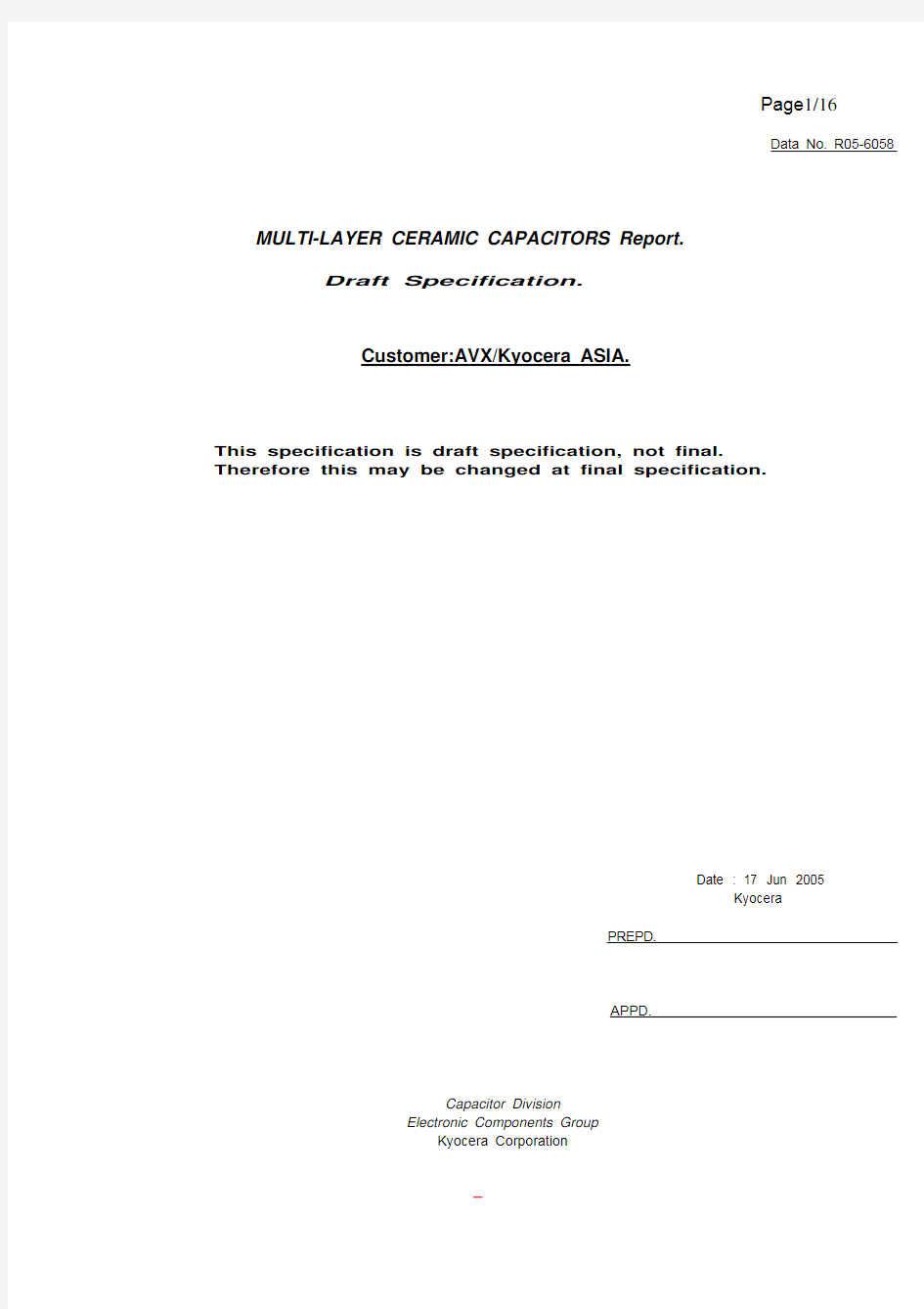
MULTI-LAYER CERAMIC CAPACITORS Report.
Draft Specification.
Customer:AVX/Kyocera ASIA.
This specification is draft specification, not final.
Therefore this may be changed at final specification.
Date : 17 Jun 2005
Kyocera
PREPD.
APPD.
Capacitor Division
Electronic Components Group
Kyocera Corporation
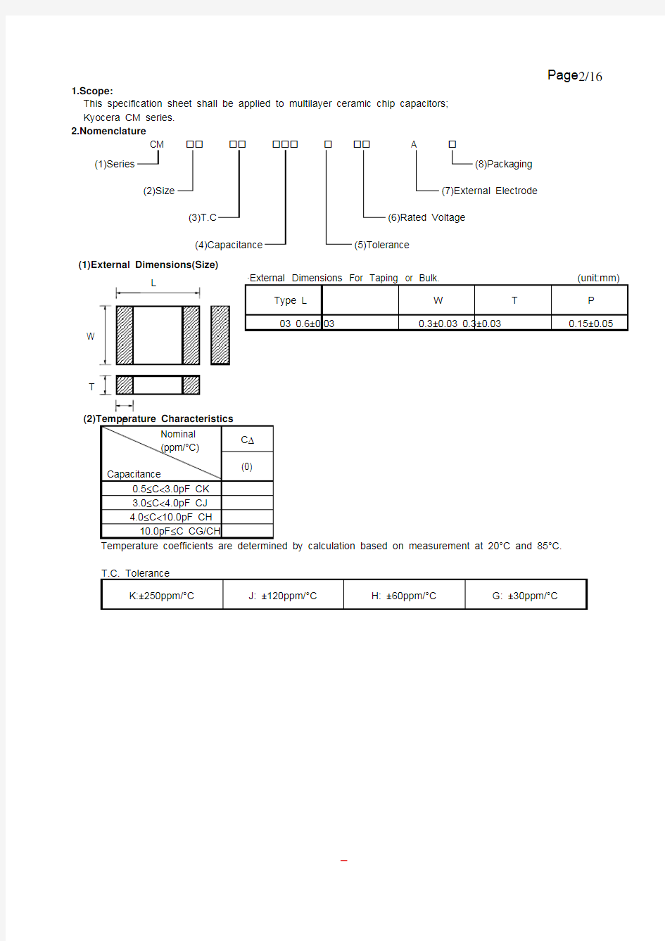
1.Scope:
This specification sheet shall be applied to multilayer ceramic chip capacitors; Kyocera CM series. 2.Nomenclature
CM A
(1)Series
(8)Packaging
(2)Size
(7)External Electrode
(3)T.C
(6)Rated Voltage
(4)Capacitance
(5)Tolerance
(1)External Dimensions(Size)
·External Dimensions
For Taping or Bulk. (unit:mm)Type L W T P 03 0.6±0.03 0.3±0.03 0.3±0.03 0.15±0.05
T.C. Tolerance
K:±250ppm/°C
J: ±120ppm/°C
H: ±60ppm/°C
G: ±30ppm/°C
T
(3)Capacitance Value
Capacitance is indentified by three numbers and a letter (see example as follows).
The first and second digits indicate the first two significant figures,and the final digit is a base 10 logarithmic multiplier in picofarads.When the nominal value is less than 10pF,the letter “R” is used to indicate the decimal point.The succeeding digit(s) of the group represent significant figure(s).
[Capacitance Range for Nickel Barrier Termination]
Characteristic C?
Type Thickness(mm) 25V
03
0.3±0.03 MIN
MAX
R50
330
[Capacitance Series]
C≥10pF E-12 series
C<10pF 0.5,1,2,3,4,5,6,7,8,9 (pF)
(4) Tolerance
Code C D F J K
Tolerance ±0.25pF ±0.5pF ±1pF ±5% ±10%
Nominal C<10pF C≥10pF
(5) Rated Voltage
Code 16 25 50
Voltage 16VDC 25VDC 50VDC
(6) Termination (External Electrode)
A:NICKEL
BARRIER
(7) Packaging Configuration
Code Packaging
Configuration Applying
Size
B Bulk All
H Taping(2mm
Pitch.φ178 Reel)Refer to Taping specification
3.Operating temperature range
-55 to +125°C
4.Specifications and Test Methods
Item Specification
Measuring
Conditions
Temperature
Characteristics
Refer to Item 2-(2) Capacitance Within specified tolerance value Q(C:Nominal Capacitance) C≥30pF : Q≥1000
C<30pF : Q≥400+20C C≤1000pF:1MHz±10%,0.5 to 5Vrms C>1000pF:1kHz±10%,0.5 to 5Vrms C:Nominal capacitance
(*1)Insulation Resistance 10000M? or 500M?·μF,whichever
is less After charging with the rated voltage for 1 minutes at room temperature and normal humidity.
(*1)Dielectric Strength Resist to the high voltage Applying 3.0 times of the rated
voltage for 1 to 5 seconds,
The applied current must be controlled
under 50mA.
Appearance No serious defect Under Microscope ×10
End Termination Adherence No evidence of peeling
on the end termination
After soldering chip capacitors on
glass epoxy boards and applying
2N as shown by the arrow
mark in the sketch peeling or any
sign of peeling should not be
found on end terminations.
(Refer to Fig.1)
Appearance No serious defect
Capacitance Variation Within specified tolerance value
Resistance To Vibration
Q(Nominal Capacitance) C≥30pF : Q≥1000
C<30pF : Q≥400+20C
Vibration frequency:10 to 55 (Hz)
Swing width :1.5mm
Sweep :10→55→10
Hz/1min
x,y,z axis 2 hours/each
Total 6 hours
(Refer to Fig.2)
Appearance No serious defect
Capacitance
Variation
±2.5% or ±0.25pF,whichever is larger
Q(Nominal Capacitance) C≥30pF : Q≥1000
C<30pF : Q≥400+20C
(*1)Insulation Resistance 10000M? or 500M?·μF,whichever is less
Resistance to
Solder Leaching
(*1)Dielectric Strength Resist to the high voltage
After dipped in solder solution,
at 260±5°C for 10±0.5 seconds
and kept at room temperature and
normal humidity for 24±2 hours,
the part will satisfy the specifications.
*Pre-heat before immersion
1st: 80°C to 100°C for 120sec.
2st:150°C to 200°C for 120sec.
Solderability Coverage
≥ 90%
Each termination end After dipped in solder solution,at
235±5°C for 2±0.5 seconds and cooled gradually at room temperature and normal humidity.
(Pb Free)
After dipped in solder solution,at
245±5°C for 3±0.5 seconds and cooled gradually at room temperature and normal humidity.
(*1)Insulation Resistance/Dielectric Strength;Charging or discharging current for these tests is limited under 50mA.
1.Scope:
This specification sheet shall be applied to multilayer ceramic chip capacitors;Kyocera CM series.
2.Nomenclature
CM A (1)Series
(8)Packaging
(2)Size
(7)External Electrode (3)T.C
(6)Rated Voltage
(4)Capacitance
(5)Tolerance
(1)External Dimensions(Size)
·External Dimension for Taping or Bulk (unit:mm)Type L W T P 03 0.6±0.03 0.3±0.03 0.3±0.03 0.15±0.05
(2)Temperature Characteristics
Characteristics Applied voltage
Change
in capacitance
Operating
temperature range
Reference
No applied voltage Within +/-10% B
1/2 rated voltage Within +10/-30% -25°C~+85°C 20°C No applied voltage Within +/-15% R 1/2 rated voltage Within +15/-40% -55°C~+125°C 20°C X5R No applied voltage Within +/-15% -55°C~+85°C W5R
X7R No applied voltage Within +/-15% -55°C~+125°C 25°C
No applied voltage Within +22/-82% -30°C~+85°C
25°C
No applied voltage Within +30/-80% Y5V
F
1/2 rated voltage
Within +30/-95%
-25°C~+85°C 20°C
P T
(3)-1. Capacitance Value
Capacitance is indentified by three numbers and a letter (see example as follows). The first and second digits indicate the first two significant figures,and the final digit is a base 10 logarithmic multiplier in picofarads.
[Capacitance Series]
W5R(B,R,X5R,X7R) E- 6 Series
[Capacitance Range]
[Capacitance Series]
B(X5R) E- 6 Series
[Capacitance Series]
Series
Y5V(F) E-3
(4) Tolerance
W5R(B,R,X5R,X7R)
Code K M
Tolerance ±10% ±20%
Y5V(F)
Code Z
Tolerance +80/-20%
(5) Rated Voltage
Code 06 10 16 25 50 100 200 Voltage 6.3VDC 10VDC 16VDC 25VDC 50VDC 100VDC 200VDC
(6) Termination (External Electrode)
A:NICKEL
BARRIER
(7) Packaging Configuration
Configuration Applying
Size Code Packaging
B Bulk All
Pitch.φ178 Reel)Refer to Taping specification
H Taping(2mm
3.Operating temperature range
Refer to Item 2-(2)
4.Specifications and Test Methods
(Table 1-1)
Specification Item
W5R(B,R,X5R,X7R)
Measuring Conditions
Temperature Characteristics
Refer to Item 2-(2)
Capacitance Within specified tolerance value tan δ (*1)Less than 3.5%
(*2)Less than 5.0%
(*3)Less than 7.0% High Temperature Treetment (Table 2)
Measuring frequency
1kHz±10%
Measuring voltage 1.0±0.2Vrms (*5)nsulation Resistance
10000M ? or 500M ?·μFmin,whichever
is less
Measure after charging with the rated voltage within 2 minutes at room conditions.
(*5)Dielectric Strength
No problem observed
Applying 2.5 times of the rated voltage for 1 to 5 seconds while charging or discharging current is limited under 50mA.
Appearance
No serious defect
Under Microscope ×10
End Termination adherence No evidence of peeling on the end termination
After soldering chip capacitors on glass epoxy boards and applying 2N(0.2Kgf) as shown by the arrow mark in the sketch peeling or any sign of peeling should not be found on end terminations. (Refer to Fig.1)
Appearance No serious defect
Capacitance Variation Within specified tolerance value
Resistance to
Vibration
tan δ
Satisfies initial specified value
High Temperature Treatment (Table 2) Vibration frequency:10 to 55 (Hz) Swing width :1.5mm
Sweep :10→55→10 Hz/1min x,y,z axis 2 hours/each
Total 6 hours (Refer to Fig.2)
Appearance No serious defect Capacitance Variation Within ±7.5%
tan δ
Satisfies initial specified value
(*5)Insulation Resistance 10000M ? or 500M ?·μFmin,whichever is less Resistance to
Solder Leaching
(*5)Dielectric Strength
Resist without problem. High Temperature Treatment (Table 2)
After dipped molten solder,
at 260±5°C for 10±0.5 seconds and kept at room conditions for 48±4 hours, measure and chech the specifications.
*Pre-heat before immersion
1st: 80°C to 100°C for 120sec. 2st:150°C to 200°C for 120sec.
(*1)Applied for X7R rated voltage 16V.
(*2) Applied for X5R rated voltage 16V/25V (*3)Applied for X5R rated voltage 10V .
(*5)Insulation Resistance/Dielectric Strength;Charging or discharging current for these tests Is limited under 50mA. Note:Except the capacitance range overapped with higher rated voltage shown the above.
(Table 1-2)
(Table 2)
High Temperature Treatment Keep chip capacitor at 150°C +0/-10°C for one hour,Then leave chip capacitor at room temperature and normal humidity for 48±4 hours.
Initial
Treatment Voltage
Treatment Pretreat capacitor for 1 hour at the same condition of the load test, Then leave them at room condition for 48±4 hrs before beginning the Load test.
4.Specifications and Test Methods
(Table 1-1)
Specification
Item
Y5V(F)
Measuring Conditions
Temperature
Characteristics
Refer to Item 2-(3) Capacitance Within specified tolerance value tanδ(Dissipation factor) Less than 12.5% High Temperature Treetment (Table 2) Measuring frequency
1kHz±10%
Measuring voltage
1.0±0.2Vrms
(*4)Insulation Resistance 10000M? or 500M?·μFmin whichever
is less Measure after charging with the rated voltage within 2 minutes at room conditions.
(*4)Dielectric Strength No problem observed Applying 2.5 times of the rated
voltage for 1 to 5 seconds while
charging or discharging current is
limited under 50mA. Appearance No serious defect Under Microscope ×10
End Termination adherence No evidence of peeling
on the end termination
After soldering chip capacitors on
glass epoxy boards and applying
2N(0.2Kgf) as shown by the arrow
mark in the sketch peeling or any
sign of peeling should not be
found on end terminations.
(Refer to Fig.1)
Appearance No serious defect
Capacitance Variation Within specified tolerance value
Resistance
to
Vibration
tanδSatisfies initial specified value High Temperature Treatment (Table 2) Vibration frequency:10 to 55 (Hz) Swing width :1.5mm
Sweep :10→55→10
Hz/1min
x,y,z axis 2 hours/each
Total 6 hours (Refer to Fig.2)
Appearance No serious defect Capacitance
Variation
Within ±20%
tanδSatisfies initial specified value
(*4)Insulation Resistance 10000M? or 500M?·μFmin ,whichever is less
Resistance to
Solder Leaching
(*4)Dielectric Strength Resist without problem.
High Temperature Treatment (Table 2)
After dipped molten solder,
at 260±5°C for 10±0.5 seconds
and kept at room conditions for
48±4 hours, measure and chech
the specifications.
*Pre-heat before immersion
1st: 80°C to 100°C for 120sec.
2st:150°C to 200°C for 120sec.
(*4)Insulation Resistance/Dielectric Strength;Charging or discharging current for these tests Is limited under 50mA.
(Table 1-2)
(Table 2)
High Temperature Treatment Keep chip capacitor at 150°C +0/-10°C for one hour,Then leave chip capacitor at room temperature and normal humidity for 48±4 hours.
Initial
Treatment Voltage
Treatment Pretreat capacitor for 1 hour at the same condition of the load test, Then leave them at room condition for 48±4 hrs before beginning the Load test.
Unit:mm
type a b C
03 0.26 0.92 0.32glass epoxy board
100
Fig.3-1 Bend strength.
c
a
Fig.2 Resistance to vibration,
temperature cycling.
Fig.1 End termination
adherence (from side).
03 Size : 0.8
超级电容基本参数概念
超级电容基本参数概念 寿命Lifetime 超级电容器具有比二次电池更长的使用寿命,但它的使用寿命并不是无限的,超级电容器基本失效的形式是电容内阻的增加( ESR)与(或) 电容容量的降低.,电容实际的失效形式往往与用户的应用有关,长期过温(温度)过压(电压),或者频繁大电流放电都会导致电容内阻的增加或者容量的减小。在规定的参数范围内使用超级电容器可以有效的延长超级电容器的寿命。通常,超级电容器具有于普通电解电容类似的结构,都是在一个铝壳内密封了液体电解液,若干年以后,电解液会逐渐干涸,这一点与普通电解电容一样,这会导致电容内阻的增加,并使电容彻底失效。 电压Voltage 超级电容器具有一个推荐的工作电压或者最佳工作电压,这个值是根据电容在最高设定温度下最长工作时间来确定的。如果应用电压高于推荐电压,将缩短电容的寿命,如果过压比较长的时间,电容内部的电解液将会分解形成气体,当气体的压力逐渐增强时,电容的安全孔将会破裂或者冲破。短时间的过压对电容而言是可以容忍的。 极性Polarity 超级电容器采用对称电极设计,也就说,他们具有类似的结构。当电容首次装配时,每一个电极都可以被当成正极或者负极,一旦电容被第一次100%从满电时,电容就会变成有极性了,每一个超级电容器的外壳上都有一个负极的标志或者标识。虽然它们可以被短路以使电压降低到零伏,但电极依然保留很少一部分的电荷,此时变换极性是不推荐的。电容按照一个方向被充电的时间越长,它们的极性就变得越强,如果一个电容长时间按照一个方向充电后变换极性,那么电容的寿命将会被缩短。 温度Ambient Temperature 超级电容器的正常操作温度是-40 ℃~70℃,温度与电压的结合是影响超级电容器寿命的重要因素。通常情况下,超级电容器是温度每升高10℃,电容的寿命就将降低30%~50%,也就说,在可能的情况下,尽可以的降低超级电容器的使用温度,以降低电容的衰减与内阻的升高,如果不可能降低使用温度,那么可以降低电压以抵清高温对电容的负面影响。比如,如果电容的工作电压降低为1.8V,那么电容可以工作于65℃高温下。如果在低于室
贴片电阻规格 封装 尺寸
贴片电阻规格、封装、尺寸 ChipR Dimensions 、Footprint 简述 基本结构 分类 规格、封装、 尺寸 额定功率及工 作电压 阻值,标准阻 值 标识 规格书、生产 厂家
命名方法 价格、报价 创建时间:2005-12-30 最后修改时间:2006-10-29 贴片电阻套件 为方便学生、研发人员试验和产 品试制,特推出片式电阻系列套 件。 我们常说的贴片电阻 (SMD Resistor)叫"片式固定电阻器"(Chip Fixed Resistor),又叫"矩形片状电阻"(Rectangular Chip Resistors),是由ROHM 公司发明并最早推出市场的。特点是耐潮湿,耐高温,可靠度高,外观尺寸均匀,精确且温度系数与阻值公差小。 按生产工艺分厚膜(Thick Film Chip Resistors)、薄膜(Thin Film Chip Resistors )两种。厚膜是采用丝网印刷将电阻性材料淀积在绝缘基体(例如玻璃或氧化铝陶瓷)上,然后烧结形成的。我们通常所见的多为厚膜片式电阻,精度范围±0.5% ~ 10%,温度系数:±50PPM/℃~ ±400PPM/℃。薄膜是在真空中采用蒸发和溅射等工艺将电阻性材料淀积在绝缘基体工艺(真空镀膜技术)制
成,特点是低温度系数(±5PPM/℃),高精度(±0.01%~±1%)。 封装有:0201,0402,0603,0805,1206,1210,1812,2010,2512。其常规系列的精度为5%,1%。阻值范围从0.1欧姆到20M欧姆。标准阻值有E24,E96系列。功率有1/20W、1/16W、1/8W、1/10W、1/4W、1/2W、1W。 特性: 体积小,重量轻 适合波峰焊和回流焊 机械强度高,高频特性优越 常用规格价格比传统的引线电阻还便宜 生产成本低,配合自动贴片机,适合现代电子产品规模化生产使用状况:由于价格便宜,生产方便,能大面积减少PCB面积,减少产品外观尺寸,现在已取代绝大部分传统引线电阻。除一些小厂或不得不使用引线电阻的设计,各种电器上几乎都在使用。目前绝大部分电子产品,以0603、0805器件为主;以手机,PDA为代表的高密度电子产品多使用0201、0402的器件;一些要求稳定和安全的电子产品,如医疗器械、汽车行驶记录仪、税控机则多采用1206、1210等尺寸偏大的电阻。 市场状况:目前,在全球的市场份额中,排名依次是台湾、日本、中国、韩国,欧美几乎不再生产。主要的生产厂商几乎都在中国建立生产基地。台湾国巨(Yageo)公司为世界上第一大生产商。日本企业则生产一些如0201、0402、高精度、高电压,具有工艺难度,利润高的系列。台湾及国内工厂则多生产些
金风风力机技术参数
金风风力机技术参数
技术数据一览表 表1、GW121/2500kW机组主要技术数据编 号 项目技术参数与规格备注1 认证级别IEC IIIB及以下 2 最大风速37.5 m/s 50年一遇(10分钟平均) 3 极大风速52.5 50年一遇(3秒平均) 4 运行环境温度-30℃~+40℃ 5 生存环境温度-40℃~+50℃ 6 相对湿度≤95% 7 防护等级IP54 发电机 8 转子转速7~15.5 rpm 9 叶尖线速度85.8 m/s 10 切入风速 3 m/s 11 额定风速(静 态) 9.3 m/s 12 切出风速(10 分钟均值) 22 m/s
号 项目技术参数与规格备注 13 再启动风速风机切出后,机组持续检测风速小于切出风速(同时满足10分钟平均风速、10s持续风速、3s瞬时风速),机组即可并网。 14 再启动温度-18 ℃ 15 功率调整方式变桨变速调节 16 紧急刹车方式3个叶片顺桨实现气动刹车 17 风速-桨角关系高于额定风速变桨控制 18 风速-转速关系低于额定风速变速控制 19 噪音(整个风电 机组) <103 dB 20 轮毂中心高度90 m 21 叶轮直径121.5 m
号 项目技术参数与规格备注 22 叶片数目 3 23 扫风面积11595 m2 24 风向排列(取 向) 上风向 25 叶轮倾斜度 3 deg 26 叶片锥度-3 deg 27 叶片制造商见报价文件 28 叶片加工工艺真空吸注 29 叶片材料玻璃纤维增强树脂 30 叶片长度59.5 m 31 叶片根部连接 件 螺栓 32 叶片根部到轮 毂中心的距离 1.17 m 33 叶片纵剖面图 34 弦(根/尖)长最大弦长约3 m
电容品牌大全
电容品牌大全(转) 电容品牌大全 主板厂商惯用电容品牌 富士康Rubycon Sanyo 华擎KZG KZE 升技Rubycon 技嘉Rubycon KZG OST 磐正Sanyo OST GSC 微星KZG OST 华硕Nichicon KZG 硕泰克Sanyo Sacon 捷波GSC 七彩虹Taicon 按照Intel主板技术白皮书的介绍,主板CPU插槽附近的滤波电容单个容量最低要求为1000μF。大部分主板上常见电容的容量为2200μF,好的主板采用3500μF甚至更高容量的电容。而在Intel的原装主板上,一般单个电容容量都在3300μF以上,这就是Intel主板极其稳定的重要原因之一。可见“电容决定主板质量”这话一点不假。下面是主要电容品牌的体系图,都是从电容厂商的网站上DOWN下来的,买电容的时候可以参考一下: 目前只找到SANYO、nichicon的体系图,其它厂商只提供PDF文档,有兴趣的可以去看: SANYO: www.secc.co.jp/english/index.html nichicon: https://www.360docs.net/doc/b810969959.html, chemicon: https://www.360docs.net/doc/b810969959.html, rubycon: https://www.360docs.net/doc/b810969959.html, teapo: https://www.360docs.net/doc/b810969959.html,
OST: https://www.360docs.net/doc/b810969959.html, 总结一下,比较适合主板使用的电容必须是\"Low Impedance & ESR\"、\"Very Low Impedance & ESR\"、\"Ultra Low Impedance & ESR\" 且温度为105C的,Ultra的最好 SANYO:MV-WG、MV-WX、MV-SWG、MB-UWG、MB-EXR等系列 nichicon: H开头的系列,P开头的系列 chemicon: KZE、KZG系列 rubycon: YXF、YXG、ZL、ZLH、MBZ、MCZ系列 teapo: SC、SM、SZ系列 OST: RLP、RLZ系列 系列太多了,列举不完。在可选的系列中,再根据PDF的资料,选择寿命比较长的就好了,一般PC 只需在2000小时以上就差不多了,5000小时以上的一是难买,二是贵。 还有,就是不要迷信什么音响发烧电容、拆机电容等。这些电容,有的是85C的,有的不是LOW ESR 的,拆机电容有的生产日期距今已有十多年,就算再好也不能用。 一句话,适合的才是最好的。 电容厂商电容品牌 日系名厂Nichicon Rubycon KZG Sanyo KZE Panasonic 二线厂商OST Jackcon Nippon Teapo Taicon 其他厂商Sacon GSC Chocon Fcon 一线电容: Sanyo----三洋电容 Rubycon---红宝石 Nichicon --日系电容 KZG-------日系电容日本化工,Nippon Chemi-con
常用元器件封装尺寸大小
封装形式图片国际统一简称 LDCC LGA LQFP PDIP TO5 TO52 TO71 TO71 TO78 PGA Plastic PIN Grid Array 封装形式图片国际统一简称 TSOP Thin Small OUtline Package QFP Quad Flat Package PQFP 100L QFP Quad Flat Package SOT143 SOT220 Thin Shrink Qutline Package uBGA Micro Ball Grid Array uBGA Micro Ball Grid Array PCDIP
PLCC LQFP LQFP 100L TO8 TO92 TO93 T099 EBGA 680L QFP Quad Flat Package TQFP 100L ZIP Zig-Zag Inline Packa SOT223 SOT223 SOT23 SOT23/SOT323 SOT25/SOT353 SOT26/SOT363 FBGA FDIP SOJ
SBGA LBGA 160L PBGA 217L Plastic Ball Grid Array SBGA 192L TSBGA 680L CLCC SC-705L SDIP SIP Single Inline Package SO Small Outline Package SOP EIAJ TYPE II 14L SSOP 16L SSOP SOJ 32L Flat Pack HSOP28 ITO220 ITO3P TO220 TO247
RVT贴片铝电解电容470UF35V 10X10规格书
Note: All design and specifications are for reference only and is subject to change without prior notice. If any doubt about safety for your application, please contact us immediately for technical assistance before purchase. 注: 以上所提供的設計及特性參數僅供參考,任何修改不作預先通知。如果在使用上有疑問,請在採購前與我們聯繫,以便提供技術上的協助。 WIDE TEMPERATURE 寬溫品 Operating with wide temperature range -40~+105°C 適用於 -40~+105°C 的寬溫範圍 Load life of 1000~2000 hours 負荷壽命1000~2000小時 Comply with the RoHS directive 符合RoHS 指令 SPECIFICATIONS 特性表 Items 項目 Characteristics 主要特性 Operation Temperature Range 使用温度範圍 -40 ~ +105°C Voltage Range 額定工作電壓範圍 4 ~ 450V Capacitance Range 靜電容量範圍 0.1 ~ 6800μ F Capacitance Tolerance 靜電容量允許偏差 ±20% at 120Hz, 20°C Leakage Current 漏電流 Rated Voltage 額定工作電壓 6.3 ~ 100V 160 ~ 450V Case size 尺寸 ?4~?10 ?12.5~?16 ?6.3~? 16 Time 時間 after 2 min. (application of rated voltage)2分鐘後(施加額定工作電壓)after 1 min. (application of rated voltage) 1分鐘後(施加額定工作電壓) after 5 min. (application of rated voltage)5分鐘後(施加額定工作電壓)Leakage current 漏電流 ≤0.01CV or 3μA, whichever is greater ≤0.01CV 或3μA ,取較大值 ≤0.03CV or 4μA, whichever is greater ≤0.03CV 或4μA ,取較大值 ≤0.04CV+100μA, whichever is greater ≤0.04CV+100μA ,取較大值 Dissipation Factor (tan δ) 損耗角正切 Measurement frequency 測試頻率: 120Hz, Temperature 温度: 20°C Rated Voltage (V) 額定工作電壓 4 6.3101625 3550 63 100 160~250350~450tan δ (max.) 最大損耗角正切 ?4~?10 0.420.300.260.220.160.14 0.12 0.10 0.100.20 0.25 ?12.5~?160.450.380.340.300.26 0.22 0.18 0.14 0.100.20 0.25 Stability at Low Temperature 低溫特性 Measurement frequency 測試頻率: 120Hz Rated Voltage (V) 額定工作電壓 4 6.3101625 35 50~63 100160~250350~450 Impedance Ratio 阻抗比 ZT/Z20 (max.) ?4~?10 Z(-25°C)/Z(20°C)7 4 3 2 2 2 2 3 2 3 Z(-40°C)/Z(20°C)158 6 4 4 3 3 4 3 6 ?12.5~?16 Z(-25°C)/Z(20°C)7 5 4 3 2 2 2 2 2 4 Z(-40°C)/Z(20°C)1712108 5 4 3 3 6 10 Load Life 高溫負荷特性 After 2000 hrs. (1000 hrs. for ?4~?6.3×5.4) application of the rated voltage at 105°C, they meet the characteristics listed below. 在105°C 環境中施加額定工作電壓2000小時(?4~?6.3×5.4為1000小時)後,電容器的特性符合下表的要求。 Capacitance Change 靜電容量變化率 Within ±20% of initial value for capacitors of 10V or more (Within ±30% of initial value for capacitors of 4V or less) ≥10V 為初始值的±20%以內(≤4V 為初始值的±30%以內) Dissipation Factor 損耗角正切 200% or less of initial specified value 不大於規範值的200% Leakage Current 漏電流 initial specified value or less 不大於規範值 Shelf Life 高溫貯存特性 After leaving capacitors under no load at 105°C for 1000 hours, they meet the specified value for load life characteristics listed above. 在105°C 環境中無負荷放置1000小時後,電容器的特性符合高溫負荷特性中所列的規定值。 Resistance to Soldering Heat 耐焊接熱特性 After reflow soldering and restored at room temperature, they meet the characteristics listed below. 經過回流焊並冷卻至室溫後,電容器的特性符合下表的要求。 Capacitance Change 靜電容量變化率 Within ±10% of initial value 初始值的±10%以内 Dissipation Factor 損耗角正切 initial specified value or less 不大於規範值 Leakage Current 漏電流 initial specified value or less 不大於規範值 Marking 標識 Black print on the case top. 鋁殼頂部黑字印刷。 DRAWING (Unit: mm) 外形圖 *1. Voltage mark for 6.3V is [6V] *2. Applicable to ?6.3×7.7 *3. Applicable to ?8×10.5~?10 *4. Applicable to ?12.5~?16 6.3V 的產品標識為 [6V] 適用於?6.3×7.7 適用於?8×10.5~?10 適用於?12.5~?16 Series SMD aluminum electrolytic capacitor东莞市合粤电子有限公司www.heyuecap.com
蓄电池基本知识(参数含义及各型号优缺点)
电池基本参数说明 额定电压:电池正常工作的电压。 额定容量:例如:28Ah(20hr,1.75V/cell,25℃) 是指在25℃时,20小时放电(即2.8A)使单个电池电压降到1.75V所放出的容量,折算到1小时放电的安培值。 尺寸:长、宽、高、总高。 内阻:例如:4.0mΩ(25℃,充满电) CCA:冷启动电流值:在-17.8℃和-28.9℃条件下,充满电的12V蓄电池在30s 内,其端电压下降到7.2V时,蓄电池所能供给的最小电流。 储备容量(25℃):完全充足电的12V蓄电池,在25±2℃的条件下,以25A恒流放电至蓄电池端电压下降到10.5±0.05V时的放电时间。 环境温度:电池工作的温度,有的细分充电温度与放电温度。 DODxx%:电池用掉xx%的电。如:“DOD80%,700次”则说明电池每次都用去80%的电,可循环使用700次。 最大充电电流:例如:4.5C20。是指在以20小时放电为标准的电池容量数值乘以4.5即为最大充电电流。 最大放电电流:算法同上,即为最大的放电电流。 循环充电电压:也有叫浮充电压,是指将蓄电池组与电源线路并联连接到负载电路上,电源线路仅略高于蓄电池组的断路电压,由电源线路所供的少量电流来补偿蓄电池组局部作用的损耗,以使其能经常保持在充电满足状态而不致过充电。电极L或R:有正极、反极电池之分。区分方法: 1、在外包装或者电池上,反极电池一般会标注"L"字样。正极电池一般不标注。 2、面对电池极柱靠近自己一侧,正极电池‘+’极柱在电池左侧,反之在右侧。比能量: 体积能量密度:以wh/L为单位,体现单位体积下电池可以存储的能量大小。 重量能量密度:以wh/kg为单位,体现单位重量下电池可以存储的能量大小。比功率:以kw/kg为单位,体现单位重量下电池可以输出的功率。 电池三段式充电 一、恒流段:当电池电压较低时,为了避免充电电流过大损坏电池,应该限制充电电流不能过大,又为了缩短充电时间,应使用最大允许充电电流充电。恒流充电阶段为主充电阶段,电池已经充入约85~90%的电量。 二、恒压段:保持这个恒定的电压对电池充电,在恒压充电过程中,电池电压会越来越高,电流会越来越小,当充电电流下降到0.5C时,恒压充电结束。 三、浮充段:浮充电阶段实际上也是恒压充电,在这个阶段的充电电压一般控制在13.6~13.8V左右,充电电流较自放电电流略大,一般为0.01~0.03C左右。通过涓流充电,可以将电池电量充到接近100%。 铅蓄电池外壳文字说明 例如:6-QAW-100-D 6:代表串联的电池数,每个2V,即12V
电容封装尺寸
电解电容:可分为无极性和有极性两类,无极性电容下述两类封装最为常见,即0805、0603;而有极性电容也就是我们平时所称的电解电容,一般我们平时用的最多的为铝电解电容,由于其电解质为铝,所以其温度稳定性以及精度都不是很高,而贴片元件由于其紧贴电路版,所以要求温度稳定性要高,所以贴片电容以钽电容为多,根据其耐压不同,贴片电容又可分为A、B、C、D四个系列,具体分类如下: 类型封装形式耐压 A 3216 10V B 3528 16V C 6032 25V D 7343 35V无极性电容的封装模型为RAD系列,例如“RAD-0.1”“RAD-0.2”“RAD-0.3”“RAD-0.4”等,其后缀的数字表示封装模型中两个焊盘间的距离,单位为“英寸”。电解电容的封装模型为RB系列,例如从“RB-.2/.4”到“RB-.5/.10”,其后缀的第一个数字表示封装模型中两个焊盘间的距离,第二个数字表示电 容外形的尺寸,单位为“英寸”。 1.电阻电容的封装形式如何选择,有没有什么原则?比如,同样是104的电容有0603、0805的封装, 同样是10uF电容有3216,0805,3528等封装形式,选择哪种封装形式比较合适呢? 我看到的电路里常用电阻电容封装: 电容: 0.01uF可能的封装有0603、0805 10uF的封装有3216、3528、0805 100uF的有7343 320pF封装:0603或0805 电阻: 4.7K、10k、330、33既有0603又有0805封装 请问怎么选择这些封装? 2.有时候两个芯片的引脚(如芯片A的引脚1,芯片B的引脚2)可以直接相连,有时候引脚之间(如A-1和B-2)之间却要加上一片电阻,如22欧,请问这是为什么?这个电阻有什么作用?电阻阻值如何选择? 3.藕合电容如何布置?有什么原则?是不是每个电源引脚布置一片0.1uf?有时候看到0.1uf和10uf 联合起来使用,为什么?
超级电容规格书
WRITTEN CHECKED APPROVED To. : DATE : 200 . . . SPECIFICATION PRODUCT : STARCAP MODEL : DMS series KORCHIP CORP. KORCHIP B/D, 817-38, Anyang 2-dong, Manan-gu, Anyang-si, Gyeonggi-do, KOREA TEL : 82 - 31 - 361 - 8000 FAX : 82 - 31 - 361 - 8080
Page No.ITEM etc. 1Cover Page 2Index 3 1. Scope 2. Part Number System 3. Product Model Name 4. Photo 5. Nominal Specifications 4 6. Cell Structure 7. Product Construction And Dimension 5 8. Packing Specifications 6 9. Specifications And Test Method 7 10. Measuring Method Of Characteristics 8 11. Mounting And Soldering 9 12. Cautions For Use 10 13. Environmental Management Index
Items DMS 3R3 204 R DMS 3R3 224 R Cell Size ?6.8 × 1.4mm ?6.8 × 1.4mm OPERATING TEMPERATURE -10 ~ +60 ℃-10 ~ +60 ℃RATED VOLTAGE 3.3 VDC 3.3 VDC ELECTROSTATIC CAPACITANCE (F) 0.20 F 0.22 F CAPACITANCE TOLERANCE -20 ~ 80 %-20 ~ 80 %EQUIVALENT SERIES RESISTANCE (ESR)LESS THAN 200?LESS THAN 200?LEAKAGE CURRENT (LC) LESS THAN 150? LESS THAN 150? 1. Scope This specification applies to STARCAP(Electric Double Layer Capacitor), submitted to specified customer in cover page. 2. Part Number System DMS 3R3 204 R (Example) ① ② ③ ④ ① Series Name ② Rated Voltage : 3.3VDC ③ Capacitance : 0.20 F (204 = 20 × 10+4 uF) ④ Terminal Type : R-type 3. Product Model Name 1) Product : Electric Double Layer Capacitor 2) Model name : DMS3R3204R, DMS3R3224R 4. Photo 5. Nominal Specifications
贴片电容封装尺寸
7343 7227 (
“钽贴片电解电容有黑色或灰色标志的一头是正极,另外一头是负极。对于铝贴片电解电容就和普通直插电解电容一样,有杠杠的那端为负极。” 在网上查到这么一句话,可算是把板子上的钽电解全部平反了! 之前在复位电路总是不正常,查来查去,是复位的钽电解极性接反了! 以往用贴片电解大都就是对付钽电解电容,隐约在意识里知道画杠的一边是接高电位,就没有太注意其极性的表示方法。给医疗组的一哥们问起来:“它不跟普通电解电容一样么?普通电解画白道子的一端是‘负’极啊?再或者它应该和贴片二极管一样吧?二极管也是画白道子的那头是‘负’极诶!”——歪着头一想也是!极性的标识方法也应该有个‘统一’的原则吧?于是在此后焊的板子里所有的钽电解都掉了个头…… 终究是以有电容的地方电平被拉得特别低这一现象,标志着我对电解电容极性的表示方法完全混乱。 真服了这种‘下贱’的表示方法,同样是电解电容,钽电解虽然昂贵一点,也不能搞特殊啊! 无极性电容以0805、0603两类封装最为常见; 0805具体尺寸:×× 1206具体尺寸:×× 贴片电容以钽电容为多,根据其耐压不同,又可分为A、B、C、D四个系列,具体分类如下: 类型封装形式耐压 A 3216 10V B 3528 16V C 6032 25V
D 7343 35V 贴片钽电容的封装是分为A型(3216),B型(3528), C型(6032), D型(7343),E型(7845)。 ------------------------------------- 贴片电容正负极区分 一种是常见的钽电容,为长方体形状,有“-”标记的一端为正; 另外还有一种银色的表贴电容,想来应该是铝电解。上面为圆形,下面为方形,在光驱电路板上很常见。这种电容则是有“-”标记的一端为负。 发光二极管:颜色有红、黄、绿、蓝之分,亮度分普亮、高亮、超亮三个等级,常用的封装形式有三类:0805、1206、1210 二极管:根据所承受电流的的限度,封装形式大致分为两类,小电流型(如1N4148)封装为1206,大电流型(如IN4007)暂没有具体封装形式,只能给出具体尺寸: X 3 X 电容:可分为无极性和有极性两类: 无极性电容下述两类封装最为常见,即0805、0603; 有极性电容也就是我们平时所称的电解电容,一般我们平时用的最多的为铝电解电容,由于其电解质为铝,所以其温度稳定性以及精度都不是很高,而贴片元件由于其紧贴电路版,所以要求温度稳定性要高,所以贴片电容以钽电容为多,根据其耐压不同,贴片电容又可分为A、B、C、D四个系列,具体分类如下: 类型封装形式耐压 A 3216 10V B 3528 16V C 6032 25V D 7343 35V
(整理)贴片电容的类型和特点
目录: 贴片电容的种类和特点 1 贴片电容基本结构 1 贴片电容 Class 2 EIA代码 2 贴片电容封装尺寸 3 贴片电容生产厂家 4 贴片电容分类 5 NPO电容器 5 X7R电容器 6 Z5U电容器8 Y5V电容器8 Y5V贴片电容容量范围8 贴片电容的种类和特点 单片陶瓷电容器(通称贴片电容)是目前用量比较大的常用元件,就AVX公司生产的贴片电容来讲有NPO、X7R、Z5U、Y5V等不同的规格,不同的规格有不同的用途。下面我们仅就常用的NPO、X7R、Z5U和Y5V来介绍一下它们的性能和应用以及采购中应注意的订货事项以引起大家的注意。不同的公司对于上述不同性能的电容器可能有不同的命名方法,这里我们引用的是AVX公司的命名方法,其他公司的产品请参照该公司的产品手册。 NPO、X7R、Z5U和Y5V的主要区别是它们的填充介质不同。在相同的体积下由于填充介质不同所组成的电容器的容量就不同,随之带来的电容器的介质损耗、容量稳定性等也就不同。所以在使用电容器时应根据电容器在电路中作用不同来选用不同的电容器。 贴片电容目前使用NPO、X7R、Z5U、Y5V等不同的材质规格,不同的规格有不同的用途。下面我们仅就常用的NPO、X7R、Z5U和Y5V来介绍一下它们的性能和应用以及采购中应注意的订货事项以引起大家的注意。不同的公司对于上述不同性能的电容器可能有不同的命名方法,这里我们引用的是敝司三巨电子公司的命名方法,其他公司的产品请参照该公司的产品手册。 NPO、X7R、Z5U和Y5V的主要区别是它们的填充介质不同。在相同的体积下由于填充介质不同所组成的电容器的容量就不同,随之带来的电容器的介质损耗、容量稳定性等也就不同。所以在使用电容器时应根据电容器在电路中作用不同来选用不同的电容器。 通常大家所说的贴片电容是指片式多层陶瓷电容 (Multilayer Ceramic Capacitors),简称MLCC,又叫做独石电容。 它是在若干片陶瓷薄膜坯上被覆以电极桨材料,叠合后一次烧结成一块不可分割的整体,外面再用树脂包封而成的。具有小体积、大容量、Q值高、高可靠和耐高温等优点。同时也具有容量误差较大、温度系数很高的缺点。一般用在噪声旁路、滤波器、积分、振荡电路。 常规贴片电容按材料分为COG(NPO)、X7R、Y5V,常见引脚封装有0201、0402、0603、0805、1206、1210、1812、2010。 贴片电容基本结构 多层陶瓷电容(MLCC)是由平行的陶瓷材料和电极材料层叠而成。见下图:
贴片电解电容的规格
贴片电解电容的规格→贴片电解电容详细规格书 贴片电解电容规格书: V 6.3 10 16 25 35 50 μF D×L mm Impeda nce Ω I~ mA D×L mm Impeda nce Ω I~ mA D×L mm Impeda nce Ω I~ mA D×L mm Impeda nce Ω I~ mA D×L mm Impeda nce Ω I~ mA D×L mm Impeda nce Ω I~ mA 1.0 4×5.4 5.0 50 4×5.4 5.0 50 1.5 4×5.4 5.0 50 4×5.4 5.0 50 2.2 4×5.4 5.0 50 4×5.4 5.0 50 3.3 4×5.4 5.0 50 4×5.4 5.0 50 4.7 4× 5.4 5.0 50 4×5.4 5.0 50 5×5.4 2.6 80 6.8 4×5.4 5.0 50 5×5.4 2.6 80 6.3×5.4 1.3 115 10 4×5.4 5.0 50 5×5.4 2.6 80 5×5.4 2.6 80 6.3×5.4 1.3 115 15 5×5.4 2.6 80 6.3×5.4 1.3 115 6.3×5.4 1.3 115 6.3×5.4 1.3 115 22 4×5.4 5.0 50 5×5.4 2.6 80 5×5.4 2.6 80 6.3×5.4 1.3 115 6.3×5.4 1.3 115 6.3× 7.70.8 150 33 5×5.4 2.6 80 5×5.4 2.6 80 6.3×5.4 1.3 115 6.3×5.4 1.3 115 6.3×7.70.8 150 6.3×7.70.8 150 47 5×5.4 2.6 80 6.3×5.4 1.3 115 6.3×5.4 1.3 115 6.3×7.70.8 150 6.3×7.70.8 150 8×10.50.5 220 68 6.3×5.4 1.3 115 6.3×5.4 1.3 115 6.3×7.7 0.8 150 6.3×7.70.8 150 6.3×7.70.8 150 8×10.50.5 220 100 6.3×5.4 1.3 115 6.3×7.70.8 150 6.3×7.70.8 150 6.3×7.70.8 220 8×10.50.5 220 8×10.50.5 220 150 6.3×7.70.8 150 6.3×7.70.8 150 6.3×7.70.8 150 8×10.50.5 220 8×10.50.5 220 10×10.50.3 330 220 6.3×7.70.8 150 6.3×7.70.8 150 8×10.50.5 220 8×10.50.5 220 10×10.50.3 330 10×10.50.3 330 330 6.3×7.70.8 150 8×10.50.5 220 10×10.50.3 330 10×10.50.3 330 10×10.50.3 330 470 8×10.50.5 220 8×10.50.5 220 10×10.50.3 330 10×10.50.3 330 680 8×10.50.5 220 10×10.50.3 330 10×10.50.3 330 1000 10×10.50.3 330 10×10.50.3 330 东莞市荣誉电子有限公司是一家致力於贴片电解电容器的研发、生产、配套销售的电子企业,主要从事的产品有全系贴片电容,电解电容,贴片电解电容等等。选贴片电容就在东莞荣誉电子。铝电解电容器的工作介质为通过阳极氧化的方式在铝箔表面生成一层极薄的三氧化二铝(Al2O3),此氧化物介质层和电容器的阳极结合成一个完整的体系,两者相互依存,不能彼此独立;我们通常所说的电容器,其电极和电介质是彼此独立的。电解电容器的阳极铝箔、阴极铝箔通常均为腐蚀铝箔,实际的表面积远远大于其表观表面积,这也是铝质电解电容器通常具有大的电容量的一个原因。由于采用具有众多微细蚀孔的铝箔,通常需用液态电解质才能更有效地利用其实际电极面积。 贴片电解电容技术: 贴片电解电容技术性能: 项目Items 特性 Characteristics 工作温度范围 OperatingTemperatureRange -55℃ ~+105℃ 额定电压范围 RatedVoltageRange 6.3V ~ 50V 标称电容量范围 NominalCapacitanceRange 1 ~1000μF 标称电容量允许偏差 Nominal Capacitance Tolerance ±20%(20℃,120Hz) 漏电流 Leakage Current I≤0.01C R V R or 3(μA),取较大者(施加额定电压 2分钟) C R :标称电容量(μF) U R :额定电压(V) I≤0.01C R V R or 3(μA) Whichever is greater(After 2 minutes’ application of rated voltage C R : Nominal Capacitance (μF) U R : Rated voltages (V) 损耗角正切(tgδ)Dissipation Factor (Max) 20℃, 120Hz U R (V) 6.3 10 16 25 35 50 tgδ0.22 0.19 0.16 0.14 0.12 0.10 耐久性Load Life +105℃施加额定电压1000小时后,电容器应满足以下要求: After 1000 hours’ application of rated voltage at 105℃, the capacitor shall meet the following requirement: 电容量变化率 Capacitance Change ±20%初始值以内(≤16V:±25% 初始值以内) Within ±20% of the initial value(≤16V: within ±25% of the initial value) 损耗角正切≤ 300%初始规定值
立隆贴片电解电容规格书
E.CAP.No1.2008/2009(E) 39 SMD Aluminum Electrolytic Capacitors VE Features ? 3 ~ 16φ, 85℃, 2,000 hours assured ? C hip type large capacitance capacitors ? D esigned for surface mounting on high density PC board. ? R oHS Compliance LEAD SPACING AND DIAMETER Unit: mm φD L A B C W P ± 0.2Fig. No.3 5.3 ± 0.2 3.3 3.3 1.5 0.45 ~ 0.750.8 3 4 5.3 ± 0.2 4.3 4.3 2.0 0.5 ~ 0.8 1.0 1 5 5.3 ± 0.2 5.3 5.3 2.3 0.5 ~ 0.8 1.5 1 6.3 5.3 ± 0.2 6.6 6.6 2.7 0.5 ~ 0.8 2.0 1 6.3 7.7 ± 0.3 6.6 6.6 2.7 0.5 ~ 0.8 2.0 1 8 10 ± 0.58.48.4 3.0 0.7 ~ 1.1 3.1 1 8 10.3 ± 0.58.48.4 3.0 0.7 ~ 1.1 3.1 1 10 10 ± 0.510.410.4 3.3 0.7 ~ 1.1 4.7 1 10 10.3 ± 0.510.410.4 3.3 0.7 ~ 1.1 4.7 1 12.513.5 ± 0.513.013.0 4.8 1.1 ~ 1.4 4.4 2 12.516 ± 0.513.013.0 4.8 1.1 ~ 1.4 4.4 2 DIAGRAM OF DIMENSIONS Fig. 1 Fig. 2 16 16.5 ± 0.517.017.0 5.8 1.1 ~ 1.4 6.4 2 MARKING φD = 3 mm φD = 4 ~ 6.3mm φD = 8 ~ 10 mm φD ≧ 12.5mm
多层陶瓷电容器技术规格书
产品技术规格书 文件编号 产品名称多层陶瓷电容技术规格书 产品型号 产品图号
目录 1 目的和适用范围 2 1.1目的 2 1.2适用范围 2 2 引用和参考的相关标准 2 3 功能简述 3 4 要求 3 4.1一般要求 3 4.2电气要求 4 4.3环境试验要求 4 4.4安全要求测试10 4.5 包装、运输、贮存10 4.6质量与可靠性10 4.7 加工工艺说明10 5对供应商的要求11 5.1规范接收11 5.2提供资料和数据11 5.3产品更改通知(PCN)11 5.4质量控制要求11 5.5供应商承诺11 6资格认证11 6.1样本11 6.2样本试验11 6.3 资格认证试验12 7重要说明12 ------------------------------------------------------------------------------------------------------------------------------------------------------------ - Copyright ? 2006Xinwei Technologies Co. Ltd., All Rights Reserved
1.1 目的 物料技术规格书是描述公司外购或外协物料的受控性文件,是公司物料规范化管理的基石。其作用为: ·供应厂商进行产品设计、生产和检验的依据 ·质量部门验货、退货的依据 ·采购部进行采购的依据 ·对供应厂商产品质量进行技术认证的依据 ·研发部门选用物料的依据 本技术规格书的目的是让供应厂商了解信威通信公司对该物料在质量及其可靠性方面的要求,只有质量和可靠性两方面都100%达到要求的物料才被信威通信公司接受。信威通信公司有权取消不合格产品供应商的资格,有权在必要时修改本技术规范的有关内容,届时供应商会提前收到有关更改通知并给予适当的时间来做相应的更改。 1.2 适用范围 本规格书适用于供应厂商进行多层陶瓷电容器设计、生产以及检验,指导质量部对供应厂商提供的多层陶瓷电容器进行技术认证及进货检验,指导采购部采购合格产品,研发部在设计新产品时选用合格物料。 2引用和参考的相关标准 GB/T 2423.1-2001 电工电子产品环境试验第2部分:试验方法试验A:低温 GB/T 2423.2-2002 电工电子产品环境试验第2部分: 试验方法试验B: 高温 GB/T 2423.3-1993 电工电子产品基本环境试验规程试验Ca:恒定湿热试验方法 GB/T 2423.10-1995 电工电子产品环境试验第2部分:试验方法试验Fc和导则:振动 GB/T 3873-1983 通信设备产品包装通用技术条件 GB/T 2828.1-2003 计数抽样检验程序第1部分:按接收质量限(AQL)检索的逐批检验抽样计划 GB/T 2693-2001 电子设备用固定电容器第1部分:总规范 GB/T 5968-1996 电子设备用固定电容器第9部分:分规范2类瓷介固定电容器 ------------------------------------------------------------------------------------------------------------------------------------------------------------- Copyright ? 2006Xinwei Technologies Co. Ltd., All Rights Reserved