SMAJXXXA-TR中文资料

?
1/6
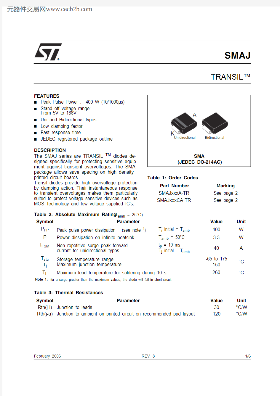
SMAJ
TRANSIL?
REV. 8
February 2006FEATURES
■Peak Pulse Power : 400 W (10/1000μs)■Stand off voltage range:From 5V to 188V
■Uni and Bidirectional types ■Low clamping factor ■Fast response time
■JEDEC registered package outline
DESCRIPTION
The SMAJ series are TRANSIL TM diodes de-signed specifically for protecting sensitive equip-ment against transient overvoltages. The SMA package allows save spacing on high density printed circuit boards.
Transil diodes provide high overvoltage protection by clamping action. Their instantaneous response to transient overvoltages makes them particularly suited to protect voltage sensitive devices such as MOS Technology and low voltage supplied IC’s.Table 2: Absolute Maximum Rating (T amb = 25°C)Table 3: Thermal Resistances
Symbol Parameter
Value
Unit P PP Peak pulse power dissipation (see note 1) T j initial = T amb 400W P Power dissipation on infinite heatsink T amb = 50°C 3.3W I FSM Non repetitive surge peak forward current for unidirectional types t p = 10 ms
T j initial = T amb
40A T stg T j Storage temperature range Maximum junction temperature
-65 to 175150°C L
Maximum lead temperature for soldering during 10 s.
°C
Note 1: for a surge greater than the maximum values, the diode will fail in short-circuit.
Symbol Parameter Value Unit Rth(j-l)Junction to leads
30°C/W Rth(j-a)Junction to ambient on printed circuit on recommended pad layout
120
°C/W
Table 1: Order Codes
Part Number Marking SMAJxxxA-TR See page 2SMAJxxxCA-TR
See page 2
SMAJ
2/6
Table 4: Electrical Characteristics (T amb = 25°C)Note 2:Pulse test : t p < 50 ms.
Note 3:?V BR = αT * (T amb - 25) * V BR (25°C).
Note 4:
V R = 0 V, F = 1 MHz. For bidirectional types, capacitance value is divided by 2.
Symbol Parameter V RM Stand-off voltage
V BR Breakdown voltage V CL Clamping voltage I RM Leakage current I PP Peak pulse current αT Voltage temperature coefficient
V F
Forward voltage drop
Types
I RM @ V RM V BR @ I R
V CL @ I PP
V CL @ I PP
αT
C max
min
note2max 10/1000μs max 8/20μs max note3
typ note4Unidirectional Mark.Bidirectional Mark. μA V V mA V A V A
10-4/°C pF SMAJ5.0A-TR AE SMAJ5.0CA-TR AA 800 5.0 6.4109.243.513.4174 5.73500SMAJ6.0A-TR DUB SMAJ6.0CA-TR DBB 800 6.0 6.71010.338.813.7170 5.93300SMAJ6.5A-TR DUC SMAJ6.5CA-TR DBC 500 6.57.21011.235.714.5160 6.13100SMAJ8.5A-TR DUH SMAJ8.5CA-TR DBH 108.59.44114.427.718.61247.32000SMAJ10A-TR AX SMAJ10CA-TR AC 51011.111723.521.71067.81550SMAJ12A-TR DUK SMAJ12CA-TR DBK 51213.3119.920.125.3918.31325SMAJ13A-TR BG SMAJ13CA-TR BH 11314.4121.518.627.2858.41200SMAJ15A-TR BM SMAJ15CA-TR AJ 11516.7124.416.432.5718.8975SMAJ18A-TR DUQ SMAJ18CA-TR DBQ 11820129.213.739.3599.2800SMAJ20A-TR DUR SMAJ20CA-TR DBR 12022.2132.412.342.8549.4725SMAJ22A-TR DUS SMAJ22CA-TR DBS 12224.4135.511.248.3489.6625SMAJ24A-TR DUT SMAJ24CA-TR DBT
12426.7138.910.350469.6600SMAJ26A-TR DUU SMAJ26CA-TR DBU 12628.9142.19.553.5439.7575SMAJ28A-TR CG SMAJ28CA-TR CH 12831.1145.48.859399.8510SMAJ30A-TR CK SMAJ30CA-TR CL 13033.3148.48.364.3369.9480SMAJ33A-TR CM SMAJ33CA-TR CN 13336.7153.37.569.73310.0450SMAJ40A-TR DUZ SMAJ40CA-TR DBZ 14044.4164.5 6.2842710.1370SMAJ43A-TR EUA SMAJ43CA-TR EBA 14347.8169.4 5.7912510.2350SMAJ48A-TR CX SMAJ48CA-TR CY 14853.3177.4 5.21002310.3320SMAJ58A-TR EUF SMAJ58CA-TR EBF 15864.4193.6 4.31211910.4270SMAJ70A-TR EUI SMAJ70CA-TR EBI 17077.81113 3.51461610.5230SMAJ85A-TR EUL SMAJ85CA-TR EBL 18594.41137 2.91781310.6200SMAJ100A-TR EUN SMAJ100CA-TR EBN 11001111162 2.52121110.7170SMAJ130A-TR EUQ SMAJ130CA-TR EBQ 11301441209 1.9265910.8145SMAJ154A-TR EUT SMAJ154CA-TR EBT 11541711246 1.6317710.8125SMAJ170A-TR SR SMAJ170CA-TR SS 11701891275 1.4353 6.510.8120SMAJ188A-TR
EUV
SMAJ188CA-TR EBV
1
188
209
1
328
1.4
388
610.8
110
SMAJ
3/6
Figure 1: Pulse waveform (10/1000μs)
Figure 2: Peak power dissipation versus initial
Figure 3: Peak pulse power versus exponential pulse duration (Tj initial=25°C)
Figure 4: Clamping voltage versus peak pulse current (Tj initial=25°C)
Figure 5: Capacitance versus reverse applied
Figure 6: Capacitance versus reverse applied
SMAJ
4/6
Figure 11: Ordering Information Scheme
Figure 7: Peak forward voltage drop versus peak forward current (typical values)
Figure 8: Relative variation of thermal impedance junction to ambient versus pulse
Figure 9: Thermal resistance junction to ambient versus copper surface under each
Figure 10: Relative variation of leakage current versus junction temperature
SMAJ
5/6
Figure 12: SMA Package Mechanical Data
E
C
L
E1
D
A1
A2
b
REF.
DIMENSIONS
Millimeters
Inches Min.
Max.Min.Max.A1 1.90 2.030.0750.080A20.050.200.0020.008b
1.25 1.650.0490.065c 0.150.410.0060.016E
4.80
5.600.1890.220E1
3.95
4.600.1560.181D 2.25 2.950.0890.116L
0.75
1.60
0.030
0.063
packages have a Lead-free second level interconnect . The category of second level interconnect is marked on the package and on the inner box label, in compliance with JEDEC Standard JESD97. The maximum ratings related to soldering conditions are also marked on the inner box label. ECOPACK is an ST trademark. ECOPACK specifications are available at: https://www.360docs.net/doc/0b1672798.html,. Table 5: Ordering Information
Part Number Marking Package Weight Base qty Delivery mode SMAJxxxA-TR See page 2SMA 0.068 g 5000Tape & reel SMAJxxxCA-TR
See page 2
SMA
0.068 g
5000
Tape & reel
Table 6: Revision History
Date Revision Description of Changes
September-19985B Previous update.
02-Aug-20046SMA package dimensions update. Reference A1 max. changed from 2.70mm (0.106inc.) to 2.03mm (0.080).10-Dec-20047Template layout update. No content change.10-Feb-2006
8
Added unidirectional marking on cover page and Figure 14. Changed Figure 13. Foot print.
SMAJ
Information furnished is believed to be accurate and reliable. However, STMicroelectronics assumes no responsibility for the consequences of use of such information nor for any infringement of patents or other rights of third parties which may result from its use. No license is granted by implication or otherwise under any patent or patent rights of STMicroelectronics. Specifications mentioned in this publication are subject to change without notice. This publication supersedes and replaces all information previously supplied. STMicroelectronics products are not authorized for use as critical components in life support devices or systems without express written approval of STMicroelectronics.
The ST logo is a registered trademark of STMicroelectronics.
All other names are the property of their respective owners
? 2006 STMicroelectronics - All rights reserved
STMicroelectronics group of companies
Australia - Belgium - Brazil - Canada - China - Czech Republic - Finland - France - Germany - Hong Kong - India - Israel - Italy - Japan - Malaysia - Malta - Morocco - Singapore - Spain - Sweden - Switzerland - United Kingdom - United States of America
https://www.360docs.net/doc/0b1672798.html,
6/6