4514中文资料
Regarding the change of names mentioned in the document, such as Mitsubishi Electric and Mitsubishi XX, to Renesas Technology Corp.
The semiconductor operations of Hitachi and Mitsubishi Electric were transferred to Renesas Technology Corporation on April 1st 2003. These operations include microcomputer, logic, analog and discrete devices, and memory chips other than DRAMs (flash memory, SRAMs etc.) Accordingly, although Mitsubishi Electric, Mitsubishi Electric Corporation, Mitsubishi Semiconductors, and other Mitsubishi brand names are mentioned in the document, these names have in fact all been changed to Renesas Technology Corp. Thank you for your understanding. Except for our corporate trademark, logo and corporate statement, no changes whatsoever have been made to the contents of the document, and these changes do not constitute any alteration to the contents of the document itself.
Note : Mitsubishi Electric will continue the business operations of high frequency & optical devices and power devices.
Renesas Technology Corp.Customer Support Dept.April 1, 2003
To all our customers
元器件交易网https://www.360docs.net/doc/0f10329312.html,
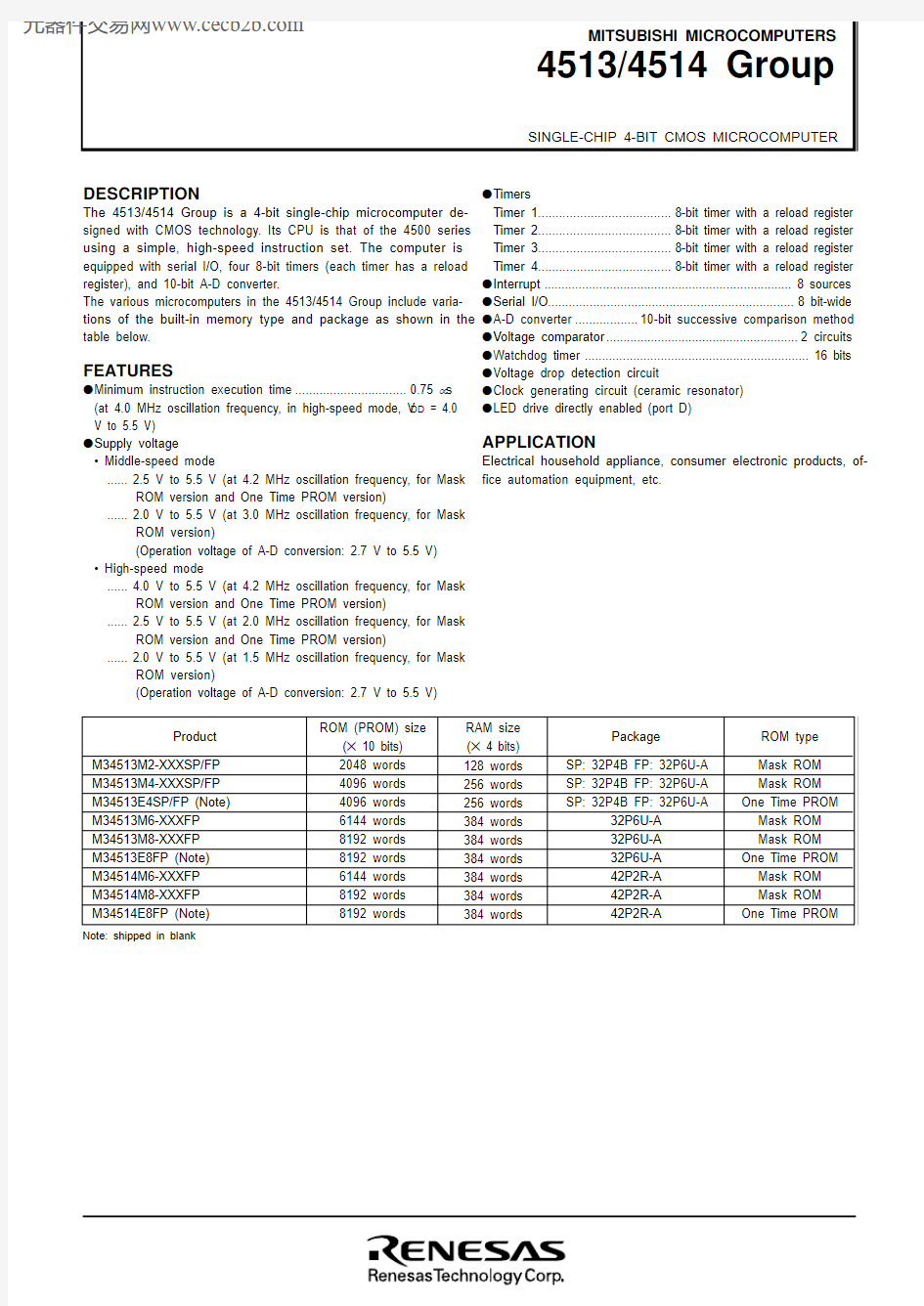
DESCRIPTION
The 4513/4514 Group is a 4-bit single-chip microcomputer de-signed with CMOS technology. Its CPU is that of the 4500 series using a simple, high-speed instruction set. The computer is equipped with serial I/O, four 8-bit timers (each timer has a reload register), and 10-bit A-D converter.
The various microcomputers in the 4513/4514 Group include varia-tions of the built-in memory type and package as shown in the table below.
FEATURES
q Minimum instruction execution time ................................0.75 μs (at 4.0 MHz oscillation frequency, in high-speed mode, V DD = 4.0V to 5.5 V)q Supply voltage
? Middle-speed mode
......2.5 V to 5.5 V (at 4.2 MHz oscillation frequency, for Mask
ROM version and One Time PROM version)
......2.0 V to 5.5 V (at 3.0 MHz oscillation frequency, for Mask
ROM version)
(Operation voltage of A-D conversion: 2.7 V to 5.5 V)
? High-speed mode
......4.0 V to 5.5 V (at 4.2 MHz oscillation frequency, for Mask
ROM version and One Time PROM version)
......2.5 V to 5.5 V (at 2.0 MHz oscillation frequency, for Mask
ROM version and One Time PROM version)
......2.0 V to 5.5 V (at 1.5 MHz oscillation frequency, for Mask
ROM version)
(Operation voltage of A-D conversion: 2.7 V to 5.5 V)
q Timers
Timer 1......................................8-bit timer with a reload register Timer 2......................................8-bit timer with a reload register Timer 3......................................8-bit timer with a reload register Timer 4......................................8-bit timer with a reload register q Interrupt ........................................................................8 sources q Serial I/O.......................................................................8 bit-wide q A-D converter ..................10-bit successive comparison method q Voltage comparator ........................................................2 circuits q Watchdog timer .................................................................16 bits q Voltage drop detection circuit
q Clock generating circuit (ceramic resonator)q LED drive directly enabled (port D)
APPLICATION
Electrical household appliance, consumer electronic products, of-fice automation equipment, etc.
Note: shipped in blank
Product
M34513M2-XXXSP/FP M34513M4-XXXSP/FP M34513E4SP/FP (Note)M34513M6-XXXFP M34513M8-XXXFP M34513E8FP (Note)M34514M6-XXXFP M34514M8-XXXFP M34514E8FP (Note)
ROM type Mask ROM Mask ROM One Time PROM Mask ROM Mask ROM One Time PROM Mask ROM Mask ROM One Time PROM
Package
SP: 32P4B FP: 32P6U-A SP: 32P4B FP: 32P6U-A SP: 32P4B FP: 32P6U-A
32P6U-A 32P6U-A 32P6U-A 42P2R-A 42P2R-A 42P2R-A
RAM size (? 4 bits)128 words 256 words 256 words 384 words 384 words 384 words 384 words 384 words 384 words
ROM (PROM) size
(? 10 bits)2048 words 4096 words 4096 words 6144 words 8192 words 8192 words 6144 words 8192 words 8192 words 4513/4514 Group
SINGLE-CHIP 4-BIT CMOS MICROCOMPUTER
BLOCK DIAGRAM (4513 Group)
BLOCK DIAGRAM (4514 Group)
PERFORMANCE OVERVIEW
Function
123128
0.75 μs (at 4.0 MHz oscillation frequency, in high-speed mode)2048 words ? 10 bits 4096 words ? 10 bits 6144 words ? 10 bits 8192 words ? 10 bits 6144 words ? 10 bits 8192 words ? 10 bits 128 words ? 4 bits 256 words ? 4 bits 384 words ? 4 bits 384 words ? 4 bits 384 words ? 4 bits 384 words ? 4 bits
Eight independent I/O ports;
ports D 6 and D 7 are also used as CNTR0 and CNTR1, respectively.
4-bit I/O port; each pin is equipped with a pull-up function and a key-on wakeup function. Both functions can be switched by software.
4-bit I/O port; each pin is equipped with a pull-up function and a key-on wakeup function. Both functions can be switched by software.
3-bit input port; ports P20, P21 and P22 are also used as S CK , S OUT and S IN , respectively.4-bit I/O port (2-bit I/O port for the 4513 Group); ports P30 and P31 are also used as INT0 and INT1, respectively. The 4513 Group does not have ports P32, P33.4-bit I/O port; The 4513 Group does not have this port.
4-bit I/O port with a direction register; The 4513 Group does not have this port.1-bit I/O; CNTR0 pin is also used as port D 6.1-bit I/O; CNTR1 pin is also used as port D 7.
1-bit input; INT0 pin is also used as port P30 and equipped with a key-on wakeup function.1-bit input; INT1 pin is also used as port P31 and equipped with a key-on wakeup function.8-bit programmable timer with a reload register.
8-bit programmable timer with a reload register is also used as an event counter.8-bit programmable timer with a reload register.
8-bit programmable timer with a reload register is also used as an event counter.10-bit wide, This is equipped with an 8-bit comparator function.2 circuits (CMP0, CMP1)8-bit ? 1
8 (two for external, four for timer, one for A-D, and one for serial I/O)1 level 8 levels
CMOS silicon gate
32-pin plastic molded SDIP (32P4B)/LQFP(32P6U-A)42-pin plastic molded SSOP (42P2R-A)–20 °C to 85 °C
2.0 V to 5.5 V for Mask ROM version, 2.5 V to 5.5 V for One Time PROM version (Refer to the electrical characteristics because the supply voltage depends on the oscillation frequency.)1.8 mA (at V DD = 5.0 V, 4.0 MHz oscillation frequency, in middle- speed mode, output transis-tors in the cut-off state)
3.0 mA (at V DD = 5.0 V,
4.0 MHz oscillation frequency, in high-speed mode, output transistors
in the cut-off state)
0.1 μA (at room temperature, V DD = 5 V, output transistors in the cut-off state)
Parameter
Number of
basic instructions
Minimum instruction execution time Memory sizes Input/Output ports
Timers
A-D converter
Voltage comparator Serial I/O
Interrupt
Subroutine nesting Device structure
Package
Operating temperature range Supply voltage
Power
dissipation (typical value)
ROM
RAM D 0–D 7
P00–P03P10–P13P20–P22P30–P33P40–P43P50–P53CNTR0CNTR1INT0INT1Timer 1Timer 2Timer 3Timer 4
Sources Nesting 4513 Group 4514 Group Active mode RAM back-up mode
4513 Group 4514 Group M34513M2M34513M4/E4M34513M6M34513M8/E8M34514M6M34514M8/E8
M34513M2
M34513M4/E4M34513M6M34513M8/E8M34514M6M34514M8/E8I/O (Input is examined by skip decision)
I/O I/O Input I/O I/O I/O I/O I/O Input Input
PIN DESCRIPTION
Name
Power supply Ground
Voltage drop detec-tion circuit enable CNV SS Reset input
System clock input System clock output I/O port D
(Input is examined by skip decision.)I/O port P0I/O port P1Input port P2I/O port P3
I/O port P4I/O port P5Analog input Timer input/output Timer input/output Interrupt input Serial data input Serial data output Serial I/O clock input/output Voltage comparator input
Voltage comparator input
Pin V DD V SS VDCE
CNV SS RESET
X IN X OUT D 0–D 7
P00–P03P10–P13P20–P22P30–P33
P40–P43P50–P53A IN0–A IN7CNTR0CNTR1INT0, INT1S IN S OUT S CK
CMP0-CMP0+CMP1-CMP1+
Input/Output
—
—Input
—I/O Input Output I/O
I/O I/O Input I/O
I/O
I/O
Input
I/O
I/O
Input
Input Output I/O
Input
Input
Function
Connected to a plus power supply.Connected to a 0 V power supply.
VDCE pin is used to control the operation/stop of the voltage drop detection circuit.When “H ” level is input to this pin, the circuit is operating. When “L ” level is inpu to this pin, the circuit is stopped.
Connect CNV SS to V SS and apply “L ” (0V) to CNV SS certainly.
An N-channel open-drain I/O pin for a system reset. When the watchdog timer causes the system to be reset or system reset is performed by the voltage drop de-tection circuit, the RESET pin outputs “L ” level.
I/O pins of the system clock generating circuit. X IN and X OUT can be connected to ceramic resonator. A feedback resistor is built-in between them.
Each pin of port D has an independent 1-bit wide I/O function. Each pin has an out-put latch. For input use, set the latch of the specified bit to “1.” The output structure is N-channel open-drain.
Ports D 6 and D 7 are also used as CNTR0 and CNTR1, respectively.
Each of ports P0 and P1 serves as a 4-bit I/O port, and it can be used as inputs when the output latch is set to “1.” The output structure is N-channel open-drain.Every pin of the ports has a key-on wakeup function and a pull-up function. Both functions can be switched by software.
3-bit input port. Ports P20, P21 and P22 are also used as S CK , S OUT and S IN , re-spectively.
4-bit I/O port (2-bit I/O port for the 4513 Group). For input use, set the latch of the specified bit to “1.” The output structure is N-channel open-drain. Ports P30 and P31 are also used as INT0 and INT1, respectively.The 4513 Group does not have ports P32, P33.
4-bit I/O port. For input use, set the latch of the specified bit to “1.” The output structure is N-channel open-drain. Ports P40–P43 are also used as analog input pins A IN4–A IN7, respectively.
The 4513 Group does not have port P4.
4-bit I/O port. Each pin has a direction register and an independent 1-bit wide I/O function. For input use, set the direction register to “0.” For output use, set the di-rection regiser to “1.” The output structure is CMOS.The 4513 Group does not have port P5.
Analog input pins for A-D converter. A IN0–A IN3 are also used as voltage compara-tor input pins and A IN4–A IN7 are also used as port P4.The 4513 Group does not have A IN4–A IN7.
CNTR0 pin has the function to input the clock for the timer 2 event counter, and to output the timer 1 underflow signal divided by https://www.360docs.net/doc/0f10329312.html,TR0 pin is also used as port D 6.
CNTR1 pin has the function to input the clock for the timer 4 event counter, and to output the timer 3 underflow signal divided by https://www.360docs.net/doc/0f10329312.html,TR1 pin is also used as port D 7.
INT0, INT1 pins accept external interrupts. They also accept the input signal to re-turn the system from the RAM back-up state.
INT0, INT1 pins are also used as ports P30 and P31, respectively.S IN pin is used to input serial data signals by software.S IN pin is also used as port P22.
S OUT pin is used to output serial data signals by software.S OUT pin is also used as port P21.
S CK pin is used to input and output synchronous clock signals for serial data trans-fer by software.
S CK pin is also used as port P20.
CMP0-, CMP0+ pins are used as the voltage comparator input pin when the volt-age comparator function is selected by software.CMP0-, CMP0+ pins are also used as A IN0 and A IN1.
CMP1-, CMP1+ pins are used as the voltage comparator input pin when the volt-age comparator function is selected by software.CMP1-, CMP1+ pins are also used as A IN2 and A IN3.
Notes 1: Pins except above have just single function.
2: The input of D 6, D 7, P20–P22, CMP0-, CMP0+, CMP1-, CMP1+ and the input/output of P30, P31, P40–P43 can be used even when CNTR0, CNTR1,S CK , S OUT , S IN , INT0, INT1, and A IN0–A IN7 are selected.3: The 4513 Group does not have P40/A IN4–P43/A IN7.
Notes 1: After system is released from reset, port P5 is in an input mode (di-rection register FR0 = 00002)
2: When the P00–P03 and P10–P13 are connected to V SS , turn off their pull-up transistors (register PU0i=“0”) and also invalidate the key-on wakeup functions (register K0i=“0”) by software. When these pins are connected to V SS while the key-on wakeup func-tions are left valid, the system fails to return from RAM back-up state. When these pins are open, turn on their pull-up transistors (register PU0i=“1”) by software, or set the output latch to “0.”
Be sure to select the key-on wakeup functions and the pull-up functions with every two pins. If only one of the two pins for the key-on wakeup function is used, turn on their pull-up transistors by software and also disconnect the other pin. (i = 0, 1, 2, or 3.)(Note when the output latch is set to “0” and pins are open)
q After system is released from reset, port is in a high-impedance state un-til it is set the output latch to “0” by software. Accordingly, the voltage level of pins is undefined and the excess of the supply current may occur while the port is in a high-impedance state.
q To set the output latch periodically by software is recommended because value of output latch may change by noise or a program run away (caused by noise).(Note when connecting to V SS and V DD )
q Connect the unused pins to V SS and V DD using the thickest wire at the shortest distance against noise.
Pin D 6D 7P20P21P22P30P31
Multifunction CNTR0CNTR1S CK S OUT S IN INT0INT1
MULTIFUNCTION
Multifunction CMP0-CMP0+CMP1-CMP1+A IN4A IN5A IN6A IN7
Pin A IN0A IN1A IN2A IN3P40P41P42P43
CONNECTIONS OF UNUSED PINS
Connection
Open (when using an external clock).Connect to V SS .
Connect to V SS , or set the output latch to “0” and open.Connect to V SS .
Connect to V SS , or set the output latch to “0” and open.
Connect to V SS , or set the output latch to “0” and open.
When the input mode is selected by soft-ware, pull-up to V DD through a resistor or pull-down to V DD .
When selecting the output mode, open.Connect to V SS .
Open or connect to V SS (Note 2)Open or connect to V SS (Note 2)
Pin
X OUT
VDCE D 0–D 5
D 6/CNTR0D 7/CNTR1P20/S CK P21/S OUT P22/S IN P30/INT0P31/INT1P32, P33
P40/A IN4–P43/A IN7P50–P53 (Note 1)
A IN0/CMP0-A IN1/CMP0+A IN2/CMP1-A IN3/CMP1+P00–P03P10–P13
Pin CNTR0CNTR1S CK S OUT S IN INT0INT1
Multifunction D 6D 7P20P21P22P30P31
Multifunction A IN0A IN1A IN2A IN3P40P41P42P43
Pin CMP0-CMP0+CMP1-CMP1+A IN4A IN5A IN6A IN7
Notes 1: The 4513 Group does not have P32 and P33.
2: The 4513 Group does not have these ports.
DEFINITION OF CLOCK AND CYCLE
q System clock
The system clock is the basic clock for controlling this product.The system clock is selected by the bit 3 of the clock control reg-ister MR.PORT FUNCTION
Port Port D
Port P0Port P1Port P2
Port P3(Note 1)Port P4(Note 2)Port P5(Note 2)
I/O unit 1
4
4
34
44
Control instructions SD, RD SZD CLD OP0A IAP0
OP1A IAP1
IAP2OP3A IAP3OP4A IAP4OP5A IAP5
Control registers W6PU0, K0
PU0, K0
J1
I1, I2
Q2FR0
Output structure N-channel open-drain
N-channel open-drain N-channel open-drain N-channel open-drain
N-channel open-drain CMOS
Input Output I/O (8)I/O (4)
I/O (4)
Input (3)I/O (4)I/O (4)I/O (4)
Remark
Built-in programmable pull-up functions
Key-on wakeup functions (programmable)
Built-in programmable pull-up functions
Key-on wakeup functions (programmable)
Built-in key-on wakeup function
(P30/INT0, P31/INT1)
Pin D 0–D 5
D 6/CNTR0D 7/CNTR1P00–P03
P10–P13
P20/S CK P21/S OUT P22/S IN P30/INT0P31/INT1P32, P33P40/A IN4–P43/A IN7P50–P53
Register MR
MR 301
System clock f(X IN )f(X IN )/2
Note: f(X IN )/2 is selected after system is released from reset.q Instruction clock
The instruction clock is a signal derived by dividing the system clock by 3. The one instruction clock cycle generates the one machine cycle.q Machine cycle
The machine cycle is the standard cycle required to execute the instruction.
Table Selection of system clock
PORT BLOCK DIAGRAMS (continued)
PORT BLOCK DIAGRAMS (continued)
PORT BLOCK DIAGRAMS (continued)
External interrupt circuit structure
CPU
(1) Arithmetic logic unit (ALU)
The arithmetic logic unit ALU performs 4-bit arithmetic such as 4-
bit data addition, comparison, AND operation, OR operation, and
bit manipulation.
(2) Register A and carry flag
Register A is a 4-bit register used for arithmetic, transfer, ex-
change, and I/O operation.
Fig. 1AMC instruction execution example
(5) Stack registers (SK S ) and stack pointer (SP)
Stack registers (SKs) are used to temporarily store the contents of program counter (PC) just before branching until returning to the original routine when;
? branching to an interrupt service routine (referred to as an inter-rupt service routine),
? performing a subroutine call, or
? executing the table reference instruction (TABP p).
Stack registers (SKs) are eight identical registers, so that subrou-tines can be nested up to 8 levels. However, one of stack registers is used respectively when using an interrupt service routine and when executing a table reference instruction. Accordingly, be care-ful not to over the stack when performing these operations together. The contents of registers SKs are destroyed when 8 lev-els are exceeded.
The register SK nesting level is pointed automatically by 3-bit stack pointer (SP). The contents of the stack pointer (SP) can be transferred to register A with the TASP instruction.Figure 5 shows the stack registers (SKs) structure.
Figure 6 shows the example of operation at subroutine call.
(6) Interrupt stack register (SDP)
Interrupt stack register (SDP) is a 1-stage register. When an inter-rupt occurs, this register (SDP) is used to temporarily store the contents of data pointer, carry flag, skip flag, register A, and regis-ter B just before an interrupt until returning to the original routine.Unlike the stack registers (SKs), this register (SDP) is not used when executing the subroutine call instruction and the table refer-ence instruction.
(7) Skip flag
Skip flag controls skip decision for the conditional skip instructions and continuous described skip instructions. When an interrupt oc-curs, the contents of skip flag is stored automatically in the interrupt stack register (SDP) and the skip condition is retained.
Fig. 5Stack registers (SKs) structure
Fig. 6Example of operation at subroutine call
Program counter (PC) is used to specify a ROM address (page and
address). It determines a sequence in which instructions stored in
ROM are read. It is a binary counter that increments the number of
instruction bytes each time an instruction is executed. However,
the value changes to a specified address when branch instructions,
subroutine call instructions, return instructions, or the table refer-
ence instruction (TABP p) is executed.
Program counter consists of PC H (most significant bit to bit 7)
which specifies to a ROM page and PC L (bits 6 to 0) which speci-
fies an address within a page. After it reaches the last address
(address 127) of a page, it specifies address 0 of the next page
(Figure 7).
Make sure that the PC H does not specify after the last page of the
built-in ROM.
(9) Data pointer (DP)
Data pointer (DP) is used to specify a RAM address and consists
of registers Z, X, and Y. Register Z specifies a RAM file group, reg-
ister X specifies a file, and register Y specifies a RAM digit (Figure
8).
Register Y is also used to specify the port D bit position.
When using port D, set the port D bit position to register Y certainly
and execute the SD, RD, or SZD instruction (Figure 9).
Fig. 9SD instruction execution example
PROGRAM MEMOY (ROM)
The program memory is a mask ROM. 1 word of ROM is composed of 10 bits. ROM is separated every 128 words by the unit of page (addresses 0 to 127). Table 1 shows the ROM size and pages. Fig-ure 10 shows the ROM map of M34514M8/E8.Table 1 ROM size and pages
Product M34513M2M34513M4/E4M34513M6M34513M8/E8M34514M6M34514M8/E8
ROM size (? 10 bits)2048 words 4096 words 6144 words 8192 words 6144 words 8192 words
Pages 16 (0 to 15)32 (0 to 31)48 (0 to 47)64 (0 to 63)48 (0 to 47)64 (0 to 63)
A part of page 1 (addresses 008016 to 00FF 16) is reserved for in-terrupt addresses (Figure 11). When an interrupt occurs, the address (interrupt address) corresponding to each interrupt is set in the program counter, and the instruction at the interrupt address is executed. When using an interrupt service routine, write the in-struction generating the branch to that routine at an interrupt address.
Page 2 (addresses 010016 to 017F 16) is the special page for sub-routine calls. Subroutines written in this page can be called from any page with the 1-word instruction (BM). Subroutines extending from page 2 to another page can also be called with the BM in-struction when it starts on page 2.
ROM pattern (bits 7 to 0) of all addresses can be used as data ar-eas with the TABP p instruction.
Fig. 10 ROM map of M34514M8/E8
Fig. 11 Page 1 (addresses 008016 to 00FF 16
) structure
DATA MEMORY (RAM)
1 word of RAM is composed of 4 bits, but 1-bit manipulation (with the SB j, RB j, and SZB j instructions) is enabled for the entire memory area. A RAM address is specified by a data pointer. The data pointer consists of registers Z, X, and Y. Set a value to the data pointer certainly when executing an instruction to access RAM.
Table 2 shows the RAM size. Figure 12 shows the RAM map. Fig. 12 RAM map Table 2 RAM size
Product
M34513M2
M34513M4/E4
M34513M6
M34513M8/E8
M34514M6
M34514M8/E8
RAM size
128 words ? 4 bits (512 bits)
256 words ? 4 bits (1024 bits)
384 words ? 4 bits (1536 bits)
384 words ? 4 bits (1536 bits)
384 words ? 4 bits (1536 bits)
384 words ? 4 bits (1536 bits)