DS90LV110_LVDS
DS90LV110AT
1to 10LVDS Data/Clock Distributor with Failsafe
General Description
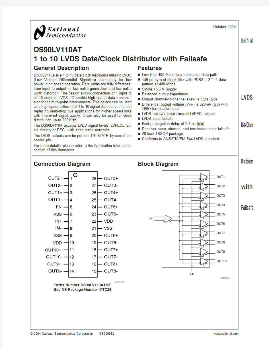
DS90LV110A is a 1to 10data/clock distributor utilizing LVDS (Low Voltage Differential Signaling)technology for low power,high speed operation.Data paths are fully differential from input to output for low noise generation and low pulse width distortion.The design allows connection of 1input to all 10outputs.LVDS I/O enable high speed data transmis-sion for point-to-point interconnects.This device can be used as a high speed differential 1to 10signal distribution /fanout replacing multi-drop bus applications for higher speed links with improved signal quality.It can also be used for clock distribution up to 200MHz.
The DS90LV110A accepts LVDS signal levels,LVPECL lev-els directly or PECL with attenuation networks.
The LVDS outputs can be put into TRI-STATE by use of the enable pin.
For more details,please refer to the Application Information section of this datasheet.
Features
n Low jitter 400Mbps fully differential data path
n 145ps (typ)of pk-pk jitter with PRBS =223?1data pattern at 400Mbps n Single +3.3V Supply
n Balanced output impedance
n Output channel-to-channel skew is 35ps (typ)
n Differential output voltage (V OD )is 320mV (typ)with 100?termination load.
n LVDS receiver inputs accept LVPECL signals n LVDS input failsafe
n Fast propagation delay of 2.8ns (typ)
n Receiver open,shorted,and terminated input failsafe n 28lead TSSOP package
n Conforms to ANSI/TIA/EIA-644LVDS standard
Connection Diagram 20098205
Order Number DS90LV110ATMT See NS Package Number MTC28
Block Diagram
20098201
October 2004
DS90LV110AT 1to 10LVDS Data/Clock Distributor with Failsafe
?2004National Semiconductor Corporation https://www.360docs.net/doc/0517252807.html,
Absolute Maximum Ratings (Note 1)
If Military/Aerospace specified devices are required,please contact the National Semiconductor Sales Office/Distributors for availability and specifications.Supply Voltage (V DD -V SS )?0.3V to +4V
LVCMOS/LVTTL Input Voltage (EN)
?0.3V to (V CC +0.3V)
LVDS Receiver Input Voltage (IN+,IN?)
?0.3V to +4V LVDS Driver Output Voltage (OUT+,OUT?)?0.3V to +4V
Junction Temperature +150?C
Storage Temperature Range ?65?C to +150?C
Lead Temperature (Soldering,4sec.)
+260?C Maximum Package Power Dissipation at 25?C 28L TSSOP
1.209W Package Derating 28L TSSOP 9.67mW/?C above +25?C
θJA
28L TSSOP 103.4?C/Watt
ESD Rating:
(HBM,1.5k ?,100pF)>4kV (EIAJ,0?,200pF)
>250V
Recommended Operating Conditions
Min Typ Max Units
Supply Voltage (V DD -V SS ) 3.0 3.3
3.6V Receiver Input Voltage
0V DD
V Operating Free Air Temperature
-40
+25+85
?C
Electrical Characteristics
Over recommended operating supply and temperature ranges unless otherwise specified Symbol Parameter
Conditions
Min Typ
Max Units LVCMOS/LVTTL DC SPECIFICATIONS (EN)
V IH High Level Input Voltage 2.0V DD V V IL Low Level Input Voltage V SS
0.8
V I IH High Level Input Current V IN =3.6V or 2.0V;V DD =3.6V ±7±20μA I IL Low Level Input Current V IN =0V or 0.8V;V DD =3.6V ±7
±20
μA V CL Input Clamp Voltage I CL =?18mA ?0.8?1.5V LVDS OUTPUT DC SPECIFICATIONS (OUT1,OUT2,OUT3,OUT4,OUT5,OUT6,OUT7,OUT8,OUT9,OUT10)
V OD Differential Output Voltage
R L =100?
250320450mV R L =100?,V DD =3.3V,T A =25?C
260
320
425mV ?V OD Change in V OD between Complimentary Output States 35|mV|V OS Offset Voltage (Note 3)
1.125
1.25
1.375V ?V OS Change in V OS between Complimentary Output States 35
|mV|I OZ Output TRI-STATE Current EN =0V,
±1±10μA V OUT =V DD or GND
I OFF Power-Off Leakage Current V DD =0V;V OUT =3.6V or GND ±1
±10
μA I SA ,I SB Output Short Circuit Current V OUT+OR V OUT?=0V or V DD 1224|mA|I SAB Both Outputs Shorted (Note 4)V OUT+=V OUT?
612|mA|LVDS RECEIVER DC SPECIFICATIONS (IN)
V TH Differential Input High Threshold V CM =+0.05V or +1.2V or +3.25V,0+100
mV V TL Differential Input Low Threshold V DD =3.3V
?1000
mV
V CMR Common Mode Voltage Range V ID =100mV,V DD =3.3V 0.05 3.25
V I IN
Input Current
V IN =+3.0V,V DD =3.6V or 0V ±1±10μA V IN =0V,V DD =3.6V or 0V
±1±10
μA
D S 90L V 110A T
https://www.360docs.net/doc/0517252807.html, 2
Electrical Characteristics(Continued)
Over recommended operating supply and temperature ranges unless otherwise specified
Symbol Parameter Conditions Min Typ Max Units SUPPLY CURRENT
I CCD Total Supply Current R L=100?,C L=5pF,200MHz,125160mA
EN=High
No Load,200MHz,EN=High80125mA I CCZ TRI-STATE Supply Current EN=Low1529mA
Note1:“Absolute Maximum Ratings”are these beyond which the safety of the device cannot be guaranteed.They are not meant to imply that the device should be operated at these limits.The table of“Electrical Characteristics”provides conditions for actual device operation.
Note2:All typical are given for V CC=+3.3V and T A=+25?C,unless otherwise stated.
Note3:V OS is defined as(V OH+V OL)/2.
Note4:Only one output can be shorted at a time.Don’t exceed the package absolute maximum rating.
AC Electrical Characteristics
Over recommended operating supply and temperature ranges unless otherwise specified.
Symbol Parameter Conditions Min Typ Max Units T LHT Output Low-to-High Transition Time,20%to80%,Figure4
(Note5)
390550ps
T HLT Output High-to-Low Transition Time,80%to20%,Figure4
(Note5)
390550ps
T DJ LVDS Data Jitter,Deterministic
(Peak-to-Peak)(Note6)V ID=300mV;PRBS=223-1data;
V CM=1.2V at400Mbps(NRZ)
145ps
T RJ LVDS Clock Jitter,Random(Note6)V ID=300mV;V CM=1.2V
at200MHz clock
2.8ps
T PLHD Propagation Low to High Delay,Figure5 2.2 2.8 3.6ns
T PHLD Propagation High to Low Delay,Figure5 2.2 2.8 3.9ns
T SKEW Pulse Skew|T PLHD-T PHLD|(Note5)20340ps
T CCS Output Channel-to-Channel Skew,Figure6(Note5)3591ps
T PHZ Disable Time(Active to TRI-STATE)High to Z,Figure1 3.0 6.0ns
T PLZ Disable Time(Active to TRI-STATE)Low to Z,Figure1 1.8 6.0ns
T PZH Enable Time(TRI-STATE to Active)Z to High,Figure110.023.0ns
T PZL Enable Time(TRI-STATE to Active)Z to Low,Figure17.023.0ns
Note5:The parameters are guaranteed by design.The limits are based on statistical analysis of the device performance over PVT(process,voltage and temperature)range.
Note6:The measurement used the following equipment and test setup:HP8133A pattern/pulse generator),5feet of RG-142cable with DUT test board and HP83480A(digital scope mainframe)with HP83484A(50GHz scope module).The HP8133A with the RG-142cable exhibit a T DJ=26ps and T RJ=1.3ps
DS90LV110AT
https://www.360docs.net/doc/0517252807.html,
3
AC Timing Diagrams
20098204
FIGURE 1.Output active to TRI-STATE and TRI-STATE to active output time
20098215
FIGURE 2.LVDS Driver TRI-STATE Circuit
20098206
FIGURE 3.LVDS Output Load
20098209
FIGURE 4.LVDS Output Transition Time
D S 90L V 110A T
https://www.360docs.net/doc/0517252807.html, 4
AC Timing Diagrams
(Continued)
20098207
FIGURE 5.Propagation Delay Low-to-High and High-to-Low
20098208
FIGURE 6.Output 1to 10Channel-to-Channel Skew
DS90LV110AT
https://www.360docs.net/doc/0517252807.html,
5
DS90LV110A Pin Descriptions
Pin Name
#of Pin
Input/Output
Description
IN+1I Non-inverting LVDS input
IN -1I Inverting LVDS input OUT+10O Non-inverting LVDS Output OUT -10O Inverting LVDS Output
EN
1
I
This pin has an internal pull-down when left open.A logic low on the Enable puts all the LVDS outputs into TRI-STATE and reduces the supply current.V SS 3P Ground (all ground pins must be tied to the same supply)
V DD
2
P
Power Supply (all power pins must be tied to the same supply)
Application Information
INPUT FAIL-SAFE
The receiver inputs of the DS90LV110A have internal fail-safe biasing for short,open,and teminated input conditions.LVDS INPUTS TERMINATION
The LVDS Receiver input must have a 100?termination resistor placed as close as possible across the input pins.UNUSED CONTROL INPUTS
The EN control input pin has internal pull down device.If left open,the 10outputs will default to TRI-STATE.
EXPANDING THE NUMBER OF OUTPUT PORTS
To expand the number of output ports,more than one DS90LV110A can be used.Total propagation delay through the devices should be considered to determine the maxi-mum expansion.Adding more devices will increase the out-put jitter due to each pass.
PCB LAYOUT AND POWER SYSTEM BYPASS
Circuit board layout and stack-up for the DS90LV110A should be designed to provide noise-free power to the de-vice.Good layout practice also will separate high frequency or high level inputs and outputs to minimize unwanted stray noise pickup,feedback and interference.Power system per-formance may be greatly improved by using thin dielectrics (4to 10mils)for power/ground sandwiches.This increases the intrinsic capacitance of the PCB power system which improves power supply filtering,especially at high frequen-
cies,and makes the value and placement of external bypass capacitors less critical.External bypass capacitors should include both RF ceramic and tantalum electrolytic types.RF capacitors may use values in the range 0.01μF to 0.1μF.Tantalum capacitors may be in the range 2.2μF to 10μF.Voltage rating for tantalum capacitors should be at least 5X the power supply voltage being used.It is recommended practice to use two vias at each power pin of the DS90LV110A as well as all RF bypass capacitor terminals.Dual vias reduce the interconnect inductance by up to half,thereby reducing interconnect inductance and extending the effective frequency range of the bypass components.
The outer layers of the PCB may be flooded with additional ground plane.These planes will improve shielding and iso-lation as well as increase the intrinsic capacitance of the power supply plane system.Naturally,to be effective,these planes must be tied to the ground supply plane at frequent intervals with vias.Frequent via placement also improves signal integrity on signal transmission lines by providing short paths for image currents which reduces signal distor-tion.The planes should be pulled back from all transmission lines and component mounting pads a distance equal to the width of the widest transmission line or the thickness of the dielectric separating the transmission line from the internal power or ground plane(s)whichever is greater.Doing so minimizes effects on transmission line impedances and re-duces unwanted parasitic capacitances at component mounting pads.
There are more common practices which should be followed when designing PCBs for LVDS signaling.Please see Appli-cation Note:AN-1108for additional information.
D S 90L V 110A T
https://www.360docs.net/doc/0517252807.html, 6
Multi-drop Applications
20098202
Point-to-Point Distribution Applications
20098203
For applications operating at data rate greater than 400Mbps,a point-to-point distribution application should be used.This improves signal quality compared to multi-drop applications due to no stub PCB trace loading.The only load is a receiver at the far end of the transmission line.Point-to-point distribution applications will have a wider LVDS bus lines,but data rate can increase well above 400Mbps due to the improved signal quality.
DS90LV110AT
https://www.360docs.net/doc/0517252807.html,
7
Typical Performance Characteristics
Output Voltage (V OD )vs.Resistive Load (R L )
Peak-to-Peak Output Jitter at V CM =+0.4V vs.VID
20098211
20098212
Peak-to-Peak Output Jitter at V CM =+1.2V vs.VID Peak-to-Peak Output Jitter at V CM =+2.9V vs.VID
2009821320098214
D S 90L V 110A T
https://www.360docs.net/doc/0517252807.html, 8
Physical Dimensions
inches (millimeters)unless otherwise noted
NS Package Number MTC28
Order Number DS90LV110ATMT (Rail quantity of 48)DS90LV110ATMTX (2500piece Tape and Reel)
National does not assume any responsibility for use of any circuitry described,no circuit patent licenses are implied and National reserves the right at any time without notice to change said circuitry and specifications.For the most current product information visit us at https://www.360docs.net/doc/0517252807.html,.LIFE SUPPORT POLICY
NATIONAL’S PRODUCTS ARE NOT AUTHORIZED FOR USE AS CRITICAL COMPONENTS IN LIFE SUPPORT DEVICES OR SYSTEMS WITHOUT THE EXPRESS WRITTEN APPROVAL OF THE PRESIDENT AND GENERAL COUNSEL OF NATIONAL SEMICONDUCTOR CORPORATION.As used herein:
1.Life support devices or systems are devices or systems which,(a)are intended for surgical implant into the body,or (b)support or sustain life,and whose failure to perform when properly used in accordance with instructions for use provided in the labeling,can be reasonably expected to result in a significant injury to the user.
2.A critical component is any component of a life support device or system whose failure to perform can be reasonably expected to cause the failure of the life support device or system,or to affect its safety or effectiveness.
BANNED SUBSTANCE COMPLIANCE
National Semiconductor certifies that the products and packing materials meet the provisions of the Customer Products Stewardship Specification (CSP-9-111C2)and the Banned Substances and Materials of Interest Specification (CSP-9-111S2)and contain no ‘‘Banned Substances’’as defined in CSP-9-111S2.
National Semiconductor Americas Customer Support Center
Email:new.feedback@https://www.360docs.net/doc/0517252807.html, Tel:1-800-272-9959
National Semiconductor
Europe Customer Support Center
Fax:+49(0)180-5308586Email:europe.support@https://www.360docs.net/doc/0517252807.html,
Deutsch Tel:+49(0)6995086208English Tel:+44(0)8702402171Fran?ais Tel:+33(0)141918790
National Semiconductor Asia Pacific Customer Support Center
Email:ap.support@https://www.360docs.net/doc/0517252807.html,
National Semiconductor
Japan Customer Support Center Fax:81-3-5639-7507
Email:jpn.feedback@https://www.360docs.net/doc/0517252807.html, Tel:81-3-5639-7560
https://www.360docs.net/doc/0517252807.html,
DS90LV110AT 1to 10LVDS Data/Clock Distributor with Failsafe