TP30-xxx Series中文资料
TP30-xxx Series
?
BIDIRECTIONAL CROWBAR PROTECTION.VOLTAGE RANGE:FROM 62V TO 270V.HOLDING CURRENT :I H =150mA min.
REPETITIVE PEAK PULSE CURRENT :I PP =30A,10/1000μs.
JEDEC REGISTERED PACKAGE OUTLINE FEATURES
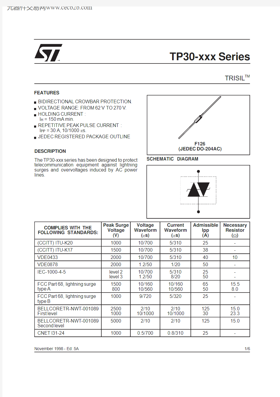
F126
(JEDEC DO-204AC)
The TP30-xxx series has been designed to protect telecommunication equipment against lightning surges and overvoltages induced by AC power lines.
DESCRIPTION
SCHEMATIC DIAGRAM
TRISIL TM
November 1998-Ed:5A
COMPLIES WITH THE FOLLOWING STANDARDS:Peak Surge Voltage (V)
Voltage Waveform (μs)Current Waveform (μs)Admissible
Ipp (A)
Necessary Resistor (?)
(CCITT)ITU-K20100010/7005/31025-(CCITT)ITU-K17150010/7005/31038-VDE0433200010/7005/3104010VDE08782000 1.2/501/2050-IEC-1000-4-5
level 2level 310/7001.2/505/3108/202550--FCC Part 68,lightning surge type A
150080010/16010/56010/16010/560655015.58.0FCC Part 68,lightning surge type B
10009/7205/32025-BELLCORETR-NWT-001089First level
250010002/1010/10002/1010/10001253015.023.3BELLCORETR-NWT-001089Second level 50002/102/1012515.0CNET l31-24
1000
0.5/700
0.8/310
25
-1/6
Symbol Parameter
Value Unit R th (j-l)Junction to leads
60°C/W R th (j-a)
Junction to ambient on printed circuit with standard footprint dimension
100
°C/W
THERMAL RESISTANCES Symbol Parameter
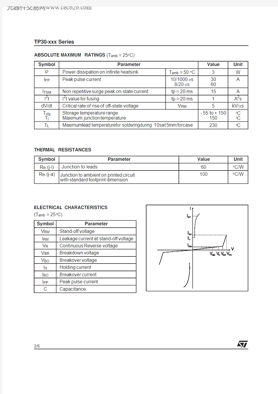
V RM Stand-off voltage
I RM Leakage current at stand-off voltage V R Continuous Reverse voltage V BR Breakdown voltage V BO Breakover voltage I H Holding current I BO Breakover current I PP Peak pulse current C
Capacitance
ELECTRICAL CHARACTERISTICS (T amb =25°C)Symbol Parameter
Value Unit P Power dissipation on infinite heatsink
T amb =50 °C 3W I PP Peak pulse current
10/1000μs 8/20μs 3060A I TSM Non repetitive surge peak on-state current tp =20ms 15A I 2t I 2t value for fusing
tp =20ms
1A 2s dV/dt Critical rate of rise of off-state voltage V RM 5
kV/μs T stg T j Storage temperature range Maximum junction temperature
-55to +150
150
°C °C T L
Maximumlead temperaturefor solderingduring 10sat 5mm forcase
230
°C
ABSOLUTE MAXIMUM RATINGS (T amb =25°C)TP30-xxx Series
2/6
Type
I RM @V RM I R @V R V BO @I BO I H C
max
max note 1
max note 2
min note 3
typ note 4
typ note 5μA
V
μA
V
V
mA
mA
pF
TP30-62TP30-68TP30-100TP30-120TP30-130TP30-180TP30-200TP30-220TP30-240TP30-270
2222222222566190108117162180198216243505050505050505050506268100120130180200220240270829013316017324026729332036080080080080080080080080080080015015015015015015015015015015050504040353530303030
20201616141412121212
Note 1:I R measured at V R guarantee V BRmin ≥V R Note 2:Measured at 50Hz (1cycle)-See test circuit 1.Note 3:See test circuit 2.Note 4:V R =1V,F =1MHz.Note 5:
V R =50V,F =1MHz.
TEST CIRCUIT 1FOR I BO and V BO parameters:
220V
static relay.
R1
R2
240
140
D.U.T
V BO measure
I BO measure
tp =20ms
K
Transformer 220V/800V
5A
Auto
Transformer 220V/2A
V out
TEST PROCEDURE :
Pulse Test duration (tp =20ms):
-For Bidirectional devices =Switch K is closed -For Unidirectional devices =Switch K is open.V OUT Selection
-Device with V BO <250Volt
-V OUT =250V RMS ,R 1=140?.
-Device with V BO ≥ 250Volt
-V OUT =480V RMS ,R 2=240?.
TP30-xxx Series
3/6
TP30-xxx Series
TEST CIRCUIT2for I H parameter.
R
-V P
D.U.T.
V BAT=-48V
Surge generator
This is a GO-NOGO Test which allows to confirmthe holding current(I H)level in a functional
test circuit.
TEST PROCEDURE:
1)Adjust the current level at the I H value by short circuiting the AK of the D.U.T.
2)Fire the D.U.T with a surge Current:Ipp=10A,10/1000μs.
3)The D.U.T will come back off-state within50ms max.
4/6
1E-2
1E-11E+0
1E+11E+21E+305101520
t(s)
ITSM(A)F =50Hz
Fig.1:Non repetitive surge peak on-sate current versus overload duration (Tj initial =25°C).
1
2
3
4
567
8
9
10
12
5
102050
VT(V)
IT(A)Tj =25°C
Fig.4:On-state voltage versus on-state current (typical values).
-40
-20020
406080100120
0.00.20.40.60.81.01.21.41.61.82.0Tj(°C)
IH[Tj]/IH[Tj=25°C]Fig.2:Relative variation of holding current versus junction temperature.
1E-3
1E-21E-1
1E+01E+11E+25E+2
1E-11E+0
1E+1
1E+2
tp(s)
Zth(j-a)(°CW)Fig.5:Variation of thermal impedance junction to ambient versus pulse duration.
1
10
100
300
0.1
0.2
0.5
1.0
VR(V)
C[VR]/C[VR=1V]F =1MHz
Fig.3:Relative variation of junction capacitance versus reverse applied voltage (typical values).
Note:ForVRM uppe r than 56V,the curve is extrapolated (dotted line)
-40
-200
20406080100
0.90
0.95
1.00
1.05
1.10Tj(°C)
Vbo[Tj]/Vbo[Tj=25°C]62V
270V
Fig.6:Relative variation of V BO voltage versus junction temperature.
TP30-xxx Series
5/6
Packaging :Tape and reel.Weight :0.40g
Information furnished is believed to be accurate and reliable.However,STMicroelectronics assumes no responsIbility for the consequences of use of such information nor for any infringement of patents or other rights of third parties which may result from its use.No license is granted by implication or otherwise under any patent or patent rights of STMicroelectronics.Specifications mentioned in this publication are subject to change without notice.This publication supersedes and replaces all information previously supplied.
STMicroelectronics products are not authorized for use as critical component s in life support devices or systems without express written ap-proval of STMicroelectronics.
The ST logo is a registered trademark of STMicroelectronics ?1998STMicroelectronics -Printed in Italy -All rights reserved.
STMicroelectronics GROUP OF COMPANIES
Australia -Brazil -Canada -China -France -Germany -Italy -Japan -Korea -Malaysia -Malta -Mexico -Morocco -The Netherlands -Singapore -Spain -Sweden -Switzerland -Taiwan -Thailand -United Kingdom -U.S.A.
https://www.360docs.net/doc/1212298591.html,
PACKAGE MECHANICAL DATA F126(Plastic)(JEDEC DO-204AC)
A
C
C
D
D
B
REF.
DIMENSIONS
Millimeters Inches Min.Typ.Max.Min.Typ.Max.
A 6.05 6.20 6.350.2380.2440.250
B 2.95 3.00
3.050.1160.1180.120C 2631
1.024
1.220
D
0.76
0.81
0.860.0300.0320.034
ORDER CODE
TP 30-62
I PP =30A
VOLTAGE
TRISIL PROTECTION
MARKING :Logo,Date Code,Part Number.TP30-xxx Series
6/6