LA317L中文资料
100mA Adustable Positive Voltage Regulator
General Description
? The LA317L is an adjustable 3-terminal positive voltage regulator capable of supplying 100mA over a 1.2V to 12V output range. This voltage regulator is exceptionally easy to use and requires only tow external resistors to set the output voltage.
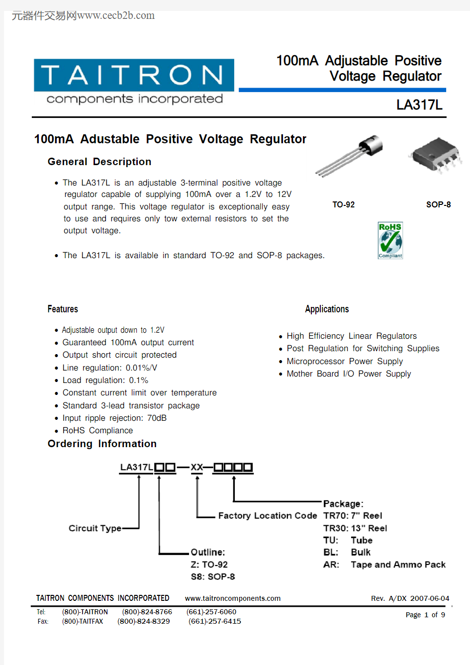
? The LA317L is available in standard TO-92 and SOP-8 packages.
Features Applications
? Adjustable output down to 1.2V ? Guaranteed 100mA output current ? Output short circuit protected ? Line regulation: 0.01%/V ? Load regulation: 0.1%
? Constant current limit over temperature ? Standard 3-lead transistor package ? Input ripple rejection: 70dB ? RoHS Compliance
Ordering Information
TO-92 SOP-8
? High Efficiency Linear Regulators
? Post Regulation for Switching Supplies ? Microprocessor Power Supply ? Mother Board I/O Power Supply
LA317L
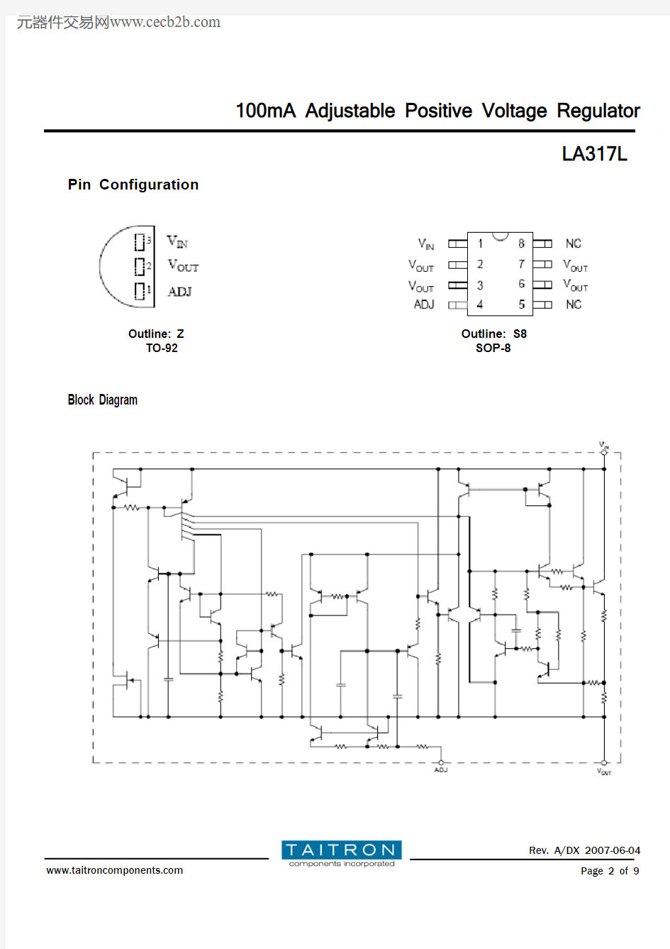
Pin Configuration
Block Diagram
Outline: Z TO-92 Outline: S8 SOP-8
LA317L
Absolute Maximum Ratings (Ta=25° C, unless otherwise specified)
Symbol Description
Ratings Unit V IN-V OUT Input - Output Voltage Differential
40 V I O Max. Output Current 100 mA T J Operating Junction Temperature 150 ° C T OPR Operating Temperature Range -20 ~ 85 ° C T STG Storage Temperature Range
-65 ~ 150 ° C P D Power Dissipation
700 mW T LEAD
Lead Temperature (Soldering, 4sec.)
260
° C
Electrical Characteristics
(V IN -V OUT =5V, I OUT =40mA,P D ≤625mW, 0oC ≤T J ≤125oC, unless otherwise specified)
LA317L
Symbol Description Min.
Typ.
Max.
Unit Conditions
- 0.01 0.04
T J =25°, 3V ≤V IN -V OUT ≤15V,
I OUT ≤20mA (Note) ?V OUT/V OUT Line Regulation
- 0.02 0.07
%/V
3V ≤V IN -V OUT ≤15V, I OUT ≤20mA
(Note)
- 0.1 0.5 % T J =25°, 5mA ≤I OUT ≤100mA (Note) ?V OUT Load Regulation - 0.3 1.5 % 5mA ≤I OUT ≤101mA (Note)
Thermal Regulation 0.04 0.2 %/W T J =25°, 10ms Pulse
I ADJ Adjustable Pin Current - 50 100 μA -
?I ADJ Adjustable Pin Current Change - 0.2 5 μA 3V ≤V IN -V OUT ≤15V,
5mA ≤I OUT ≤100mA
V REF Reference Input Voltage 1.20 1.25 1.30 V 3V ≤V IN -V OUT ≤15V, 5mA ≤I OUT ≤100mA I LIMIT Current Limit
100
200
300
mA
3V ≤V IN -V OUT ≤13V I L(MIN ) Minimum Load Current for
Regulation - 3.5 5 mA 3V ≤V IN -V OUT ≤13V
- 62 -
V OUT =10V, f=120Hz, C ADJ =0μF PSRR Ripple Rejection
60 70 - dB
V OUT =10V, f=120Hz, C ADJ =10μF
-
Temperature Stability
- 0.65 - %
0° C ≤T J ≤125° C
LA317L
Fig.1- Load Regulation vs. Temperature
Temperature (°C)Fig.3- Reference Voltage vs. Temperature Temperature (° C)
Fig.2- Output Voltage vs. Input Voltage
Input Voltage (V)
LA317L
Symbol
Description
Min.
Typ.
Max.
Unit Conditions - Long Term Stability
- 0.3 -
%
T J =125° C, 1000 Hours
- RMS Output Noise (% of V OUT ) - 0.003 - % T J =125° C, 10Hz ≤f ≤10KHz - 185 - TO-92 -
Thermal Resistance Junction to
Case
- 175 -
° C/W
SOP-8
Note: Regulation is measured at constant junction temperature, using pulse testing with a low duty cycle.
Changes in output voltage due to heating effects are covered under the specification of thermal regulation.
Typical Characteristics Curves
O u t p u t V o l t a g e D e v i a t i o n (V )
Fig.4- Adjust Pin Current vs. Temperature
Temperature (° C)
O u t p u t V o l t a g e (V )
R e f e r e n c e V o l t a g e (V )
A d j u s t P i n C u r r e n t (μA )
LA317L
Fig.5- Dropout Voltage vs. Temperature
Temperature (° C)
Fig.6- Minimum Operating Current
Input-Output Differential (V) Fig.7- Ripple Rejection vs. Output Voltage
Output Voltage (V)
Fig.8- Ripple Rejection vs. Frequency
Frequency (Hz) Typical Characteristics Curves (Continued)
I
n
p
u
t
-
O
u
t
p
u
t
D
i
f
f
e
r
e
n
t
i
a
l
(
V
)
Q
u
i
e
s
c
e
n
t
C
u
r
r
e
n
t
(
m
A
)
R
i
p
p
l
e
R
e
j
e
c
t
i
o
n
(
d
B
)
R
i
p
p
l
e
R
e
j
e
c
t
i
o
n
(
d
B
)
LA317L
Fig.9- Load Transient Response
(Conditions: V IN =10.25V, V OUT =5.25V, C IN =0.1μF,
C OUT =1μF, T A =25℃)
Time (200μs/Div) Fig.10- Line Transient Response
(Conditions: V IN =10.25 to 11.25V, I OUT =40mA, V OUT =5.25V, C IN =0.1μF, C OUT =1μF, T A =25℃)
Time (200μs/Div)
Typical Characteristics Curves (Continued)
Typical Application
ΔV O U T (200m V /D i v )
I O U T (50m A /D i v )
ΔV O U T (200m V /D i v )
ΔV I N (0.5V /D i v )
Fig.11- 5V Logic Regulator with Electronic Shutdown (Minimum output=1.2V) Fig.12- Adjustable Regulator with Improved Ripple Rejection
Note: Discharge C1 if output is shorted to ground
LA317L Typical Application (Continued)
Fig.13- Slow Turn-on 15V Regulator
Dimensions in mm (inches)
TO-92
LA317L Dimensions in mm (inches) (Continued)
SOP-8
LA317L How to contact us: