FOD3182S,FOD3182SD,FOD3182SDV,FOD3182SV,FOD3182TSR2,FOD3182TSV,FOD3182TV, 规格书,Datasheet 资料

FOD3182 — 3A Output Current, High Speed MOSFET Gate Driver Optocoupler
3A Output Current, High Speed MOSFET Gate Driver Optocoupler
Features
■ High noise immunity characterized by 50kV/μs (Typ.)common mode rejection @ V CM = 2,000V ■ Guaranteed operating temperature range of -40°C to +100°C
■ 3A peak output current ■
Fast switching speed
–210ns max. propagation delay –65ns max pulse width distortion ■ Fast output rise/fall time
–Offers lower dynamic power dissipation ■ 250kHz maximum switching speed ■ Wide V DD operating range: 10V to 30V
■
Use of P-Channel MOSFETs at output stage
enables output voltage swing close to the supply rail (rail-to-rail output)
■ 5000Vrms, 1 minute isolation
■ Under voltage lockout protection (UVLO) with hysteresis – optimized for driving MOSFETs ■ Minimum creepage distance of 8.0mm
■ Minimum clearance distance of 10mm to 16mm (option TV or TSV)
■ Minimum insulation thickness of 0.5mm ■ UL and VDE*
■
1,414 peak working insulation voltage (V IORM )
*Requires ‘V’ ordering option
Applications
■ Plasma Display Panel
■ High performance DC/DC convertor
■ High performance switch mode power supply ■ High performance uninterruptible power supply ■
Isolated Power MOSFET gate drive
Description
The FOD3182 is a 3A Output Current, High Speed MOSFET G ate Drive Optocoupler. It consists of a aluminium gallium arsenide (AlGaAs) light emitting diode optically coupled to a CMOS detector with PMOS and NMOS output power transistors integrated circuit power stage. It is ideally suited for high frequency driving of power MOSFETS used in Plasma Display Panels (PDPs), motor control inverter applications and high performance DC/DC converters.
The device is packaged in an 8-pin dual in-line housing compatible with 260°C reflow processes for lead free solder compliance.
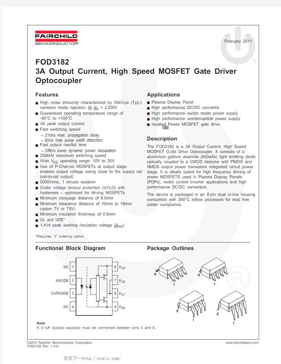
Functional Block Diagram
Package Outlines
8
1
8
1
1
23
876NC ANODE CATHODE V DD
V O2V O1
FOD3182 — 3A Output Current, High Speed MOSFET Gate Driver Optocoupler
Pin Definitions
On 7.4V to 9V 7V to 8.5V T ransition On
9V to 30V
8.5V to 30V
High
Pin #
Name
Description
1NC Not Connected 2Anode LED Anode 3Cathode LED Cathode 4NC Not Connected
5V SS Negative Supply Voltage
6V O2 Output Voltage 2 (internally connected to V O1 )7V O1 Output Voltage 18
V DD
Positive Supply Voltage
FOD3182 — 3A Output Current, High Speed MOSFET Gate Driver Optocoupler
For Rated Mains Voltage < 150Vrms I–IV
For Rated Mains Voltage < 300Vrms I–IV
For Rated Mains Voltage < 450Vrms I–III
For Rated Mains Voltage < 600Vrms I–III
For Rated Mains Voltage < 1000Vrms (Option T, TS)I–III
Climatic Classi?cation 40/100/21
Pollution Degree (DIN VDE 0110/1.89)2
CTI Comparative Tracking Index175
2651
V PR Input to Output Test Voltage, Method b,
V IORM x 1.875 = V PR, 100% Production Test with
tm = 1 sec., Partial Discharge < 5pC
Input to Output Test Voltage, Method a,
2121
V IORM x 1.5 = V PR, Type and Sample Test with
tm = 60 sec.,Partial Discharge < 5 pC
V IORM Max Working Insulation Voltage1,414V peak
V IOTM Highest Allowable Over Voltage6000V peak External Creepage8mm
External Clearance7.4mm
External Clearance (for Option T or TS - 0.4” Lead Spacing)10.16mm
Insulation Thickness0.5mm
Safety Limit Values – Maximum Values Allowed in the
Event of a Failure
T Case Case Temperature150°C
I S,INPUT Input Current25mA
P S,OUTPUT Output Power (Duty Factor ≤ 2.7%)250mW
R IO Insulation Resistance at T S, V IO = 500V109?
FOD3182 — 3A Output Current, High Speed MOSFET Gate Driver Optocoupler
Recommended Operating Conditions
The Recommended Operating Conditions table de?nes the conditions for actual device operation. Recommended operating conditions are speci?ed to ensure optimal performance to the datasheet speci?cations. Fairchild does not recommend exceeding them or designing to absolute maximum ratings.
Symbol
Parameter
Value
Units
T STG Storage T emperature -40 to +125°C T OPR Operating T emperature -40 to +100°C T J Junction T emperature
-40 to +125°C T SOL Lead Solder T emperature – Wave solder (Refer to Re?ow T emperature Pro?le, pg. 22)260 for 10 sec.
°C I F(AVG) Average Input Current (1)
25mA I F(tr, tf) LED Current Minimum Rate of Rise/Fall 250ns V R Reverse Input Voltage 5V I OH(PEAK) “High” Peak Output Current (2) 3A I OL(PEAK) “Low” Peak Output Current (2) 3A V DD – V SS Supply Voltage -0.5 to 35V V O(PEAK) Output Voltage
0 to V DD V P O Output Power Dissipation (4) 250mW P D
T otal Power Dissipation (5)
295
mW
Symbol
Parameter Value
Units
V DD – V SS Power Supply 10 to 30V I F(ON) Input Current (ON)10 to 16mA V F(OFF)
Input Voltage (OFF)
-3.0 to 0.8
V
FOD3182 — 3A Output Current, High Speed MOSFET Gate Driver Optocoupler V OH = (V DD – V SS – 6V) 2.5I OL Low Level Output Current V OL = (V DD – V SS + 1V)0.51A V OL = (V DD – V SS + 6V) 2.5V OH High Level Output Voltage(5)(6)I O = -100mA V DD – 0.5V V OL Low Level Output Voltage(5)(6)I O = 100mA V SS + 0.5V I DDH High Level Supply Current Output Open,I F = 10 to 16mA 2.6 4.0mA I DDL Low Level Supply Current Output Open,V F = -3.0 to 0.8V 2.5 4.0mA I FLH Threshold Input Current Low to High I O = 0mA, V O > 5V 3.07.5mA V FHL Threshold Input Voltage High to Low I O = 0mA, V O < 5V0.8V V F Input Forward Voltage I F = 10mA 1.1 1.43 1.8V?V F/T A T emperature Coef?cient of Forward Voltage I F = 10mA-1.5 mV/°C
V UVLO+UVLO Threshold V O > 5V, I F = 10mA78.39V
V UVLO–V O < 5V, I F = 10mA 6.57.78.5V UVLO HYST UVLO Hysteresis 0.6V BV R Input Reverse Breakdown Voltage I R = 10μA5V
C IN Input Capacitance f = 1MHz, V F = 0V25pF
C I-O Capacitance (input to output)Freq. = 1MHz1pF *Typical values at T A = 25°C
Fig. 6 Output Low Voltage vs. Ambient Temperature
V O L – O U T P U T L O W V O L T A G E (V )
0.30
0.25
0.20
0.15
0.10
0.05
V DD = 15V to 30V V SS = 0V
V F = -3V to 0.8V I O = 100mA
Fig. 5 Output Low Voltage vs. Output Low Current
V O L – O U T P U T L O W V O L T A G E (V )
4
3
21
Frequency = 200Hz Duty Cycle = 99.9%V F (off) = 0.8V V DD = 15V to 30V V SS = 0V
T A =100°C
T A = 25°C
T A = -40°C
Fig. 11 Low-to-High Input Current Threshold
vs. Ambient Temperature
-t o -H I G H I N P U T C U R R E N T T H R E S H O L D (m A )
3.6
3.4
3.2
3.0
2.8
2.6
2.4
V DD = 15V to 30V V SS = 0V
Output = Open
Fig. 12 Propagation Delay vs. Supply Voltage
t P – P R O P A G A T I O N D E L A Y (n s )
250
200
150
100
I F = 10mA to 16mA T A = 25°C R G = 10?C G = 10nF
Duty Cycle = 50%Frequency = 250kHz
t PHL t PLH
100
10
1
0.1
0.01
Fig. 18 Input Forward Current vs. Forward Voltage
I F – F O R W A R E C U R R E N T (m A )
Fig. 17 Transfer Characteristics
V O – O U T P U T V O L T A G E (V )
35
30
25
20
15
10
V DD = 30V T A = 25°C
T A =100°C
25°C -40°C
Figure 21. I OH Test Circuit
R2100?
Frequency = 200Hz Duty Cycle = 0.2%V DD = 10V to 30V V SS = 0V
I F = 10mA to 16mA
LED-IFmon
Test Conditions:
34
65
–
V = 6V
To Scope
V OH
R1100?
0.1μF
D1Current Probe
47μF
Figure 28. UVLO Test Circuit
2
V O = 5V
347
6
5
0.1μF
10V or 30V V DD Ramp
+–
I F = 10mA
45
V CM = 2,000V
?t
V CM
V O
V OH
0V
+ –
Package drawings are provided as a service to customers considering Fairchild components. Drawings may change in any manner without notice. Please note the revision and/or date on the drawing and contact a Fairchild Semiconductor representative to verify or Note:
1. All dimensions are in millimeters.
2. Dimensions are exclusive of burrs, mold fash, and tie bar extrusion.
5.08MAX
(0.78)
(0.41–0.56)
8.00 MIN 10.30 MAX
2.54 BSC
0.20–0.40
0.40 MIN Both sides 0.51 MIN
De?nitions
1Fairchild logo
2Device number
3VDE mark (Note: Only appears on parts ordered with DIN EN/IEC 60747-5-2 option – See order entry table) 4T wo digit year code, e.g., ‘11’
5T wo digit work week ranging from ‘01’ to ‘53’
6Assembly package code
R Min. Bending Radius30