ER502中文资料

ER500 THRU ER506
SUPERFAST RECOVERY RECTIFIERS
VOLTAGE - 50 to 600 Volts CURRENT - 5.0 Amperes
FEATURES
l Superfast recovery times-epitaxial construction l Low forward voltage, high current capability
l Exceeds environmental standards of MIL-S-19500/228l Hermetically sealed l Low leakage
l High surge capability
l Plastic package has Underwriters Laboratories Flammability Classification 94V-O utilizing Flame Retardant Epoxy Molding Compound MECHANICAL DA TA
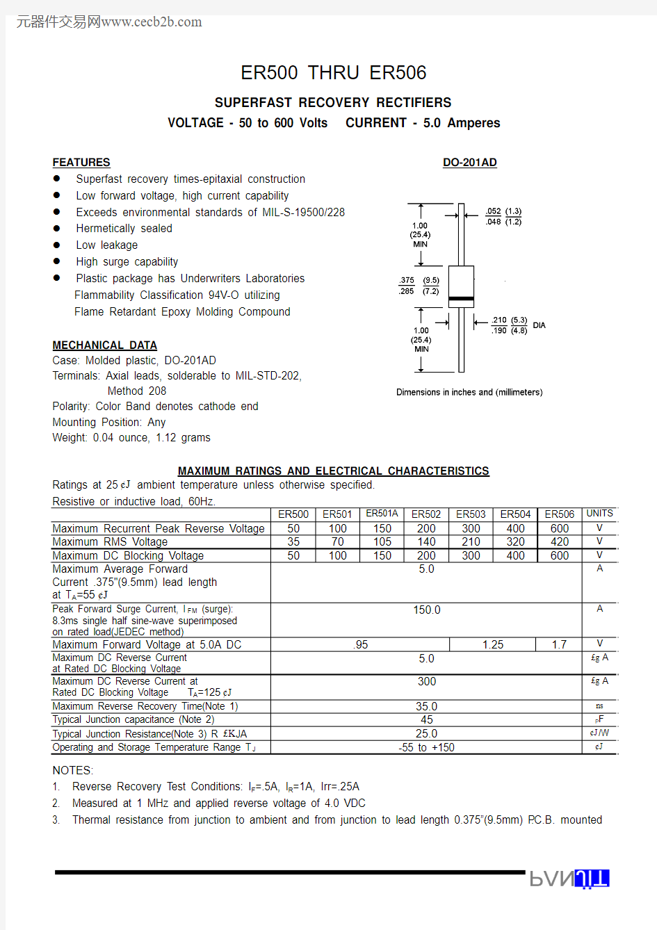
Case: Molded plastic, DO-201AD
Terminals: Axial leads, solderable to MIL-STD-202, Method 208
Polarity: Color Band denotes cathode end Mounting Position: Any
Weight: 0.04 ounce, 1.12 grams
MAXIMUM RA TINGS AND ELECTRICAL CHARACTERISTICS
Ratings at 25¢J ambient temperature unless otherwise specified.Resistive or inductive load, 60Hz.
ER500
ER501
ER501A
ER502ER503ER504ER506
UNITS Maximum Recurrent Peak Reverse Voltage 50100150200300400600V Maximum RMS Voltage
3570105140210320420V Maximum DC Blocking Voltage 50100150
200300400600
V Maximum Average Forward
Current .375"(9.5mm) lead length at T A =55¢J
5.0
A
Peak Forward Surge Current, I FM (surge):8.3ms single half sine-wave superimposed on rated load(JEDEC method)
150.0
A
Maximum Forward Voltage at 5.0A DC
.95
1.25
1.7
V Maximum DC Reverse Current at Rated DC Blocking Voltage 5.0£g A Maximum DC Reverse Current at
Rated DC Blocking Voltage T A =125¢J 300£g A Maximum Reverse Recovery Time(Note 1)35.0ns
Typical Junction capacitance (Note 2)
45P F
Typical Junction Resistance(Note 3) R £K JA 25.0¢J /W Operating and Storage T emperature Range T J
-55 to +150
¢J
NOTES:
1. Reverse Recovery T est Conditions: I F =.5A, I R =1A, Irr=.25A
2. Measured at 1 MHz and applied reverse voltage of 4.0 VDC
3. Thermal resistance from junction to ambient and from junction to lead length 0.375”(9.5mm) P .C.B. mounted
DO-201AD
RATING AND CHARACTERISTIC CURVES ER500 THRU ER506
NOTE:1.Rise Time = 7ns max.
Input Impedance = 1 megohm. 22pF 2.Rise Time = 10ns max. Source Impedance = 50 Ohms
50 ns/cm
AMBIENT TEMPERATURE, ¢J
Fig. 1-REVERSE RECOVERY TIME CHARACTERISTIC AND
TEST CIRCUIT DIAGRAM
Fig. 2-MAXIMUM AVERAGE FORWARD
CURRENT RATING
CASE TEMPERATURE, ¢J
INSTANTANEOUS FORWARD VOLTAGE, VOLTS
Fig. 3-MAXIMUM AVERAGE FORWARD CCURRENT
RATING
Fig. 4-FORWARD CURRENT DERATING CURVE
NUMBER OF CYCLES AT 60Hz
REVERSE VOLTAGE, VOLTS
Fig. 5-MAXIMUM NON-REPETITIVE SURGE CURRENT Fig. 6-TYPICAL JUNCTION CAPACITANCE