WM2200_ProductBrief_1
w
WM2200
Low Power CODEC with Enhanced Wolfson myZone?
Ambient Noise Cancellation
WOLFSON MICROELECTRONICS plc
Product Brief, June 2011, Rev 1.5
DESCRIPTION
The WM2200 is a low power mobile CODEC with enhanced
Wolfson myZone TM
Ambient Noise Cancellation (ANC). It is ideal for mobile telephony applications, providing enhanced voice communication quality for near-end and far-end handset users.
The Wolfson myZone? technology effectively reduces both stationary and non-stationary background noise. Noise reduction can be applied to receive (RX) and transmit (TX) audio paths. Full Duplex Acoustic Echo Cancellation (AEC) algorithms are also supported for Speakerphone applications.
The WM2200 is suitable for narrowband and wideband voice call applications, with direct connection from analogue or digital microphones. It can also be interfaced to baseband processors with either analogue or digital voice TX/RX signals.
The Wolfson myZone TM ANC processor implements an enhanced filtering algorithm to consistently deliver the optimum noise cancellation performance. The function is supported using two or more microphone input channels. The RX Noise reduction improves received voice intelligibility by reducing residual noise received from the far-end user during a phone call.
The TX Noise reduction and Acoustic Echo Cancellation algorithms use one or more microphone input channels as noise-compensating inputs. The WM2200 supports analogue or digital microphone inputs.
The WM2200 digital core provides extensive capability for programmable signal processing algorithms. Equalisation and application-specific filters can be implemented.
The integrated earpiece driver connects directly to the receiver earpiece in a differential (BTL) configuration. Speakerphone applications can be supported using the integrated digital speaker (PDM) interface and an external PDM-input speaker amplifier.
The device is powered from a 1.8V external supply. An integrated FLL provides support for a wide range of external clock frequencies. The WM2200 is configured using a standard 2-wire serial control interface. Fully differential internal architecture and on-chip RF noise filters ensure a very high degree of noise immunity. FEATURES
? Programmable DSP functions
? Wolfson myZone TM
adaptive ambient noise cancellation ? Transmit-path noise reduction and acoustic echo
cancellation
? Receive-path noise reduction ? Wind Noise management ? Sidetone and other programmable filters
? Audio enhancements and voice processing functions ? Audio inputs ? Up to 6 analogue or digital microphone inputs
? Single-ended or differential analogue microphone input ? Line input support (single-ended or differential) ? Earpiece output driver
? Differential (BTL) drive configuration
? Integrated Charge Pump for ground referenced output ? Dual outputs
? Hearing Aid Coil support ? Pop suppression functions
? -75dB THD+N at 20mW into 32? load
? 96dB SNR (DAC to earpiece playback, A-weighted) ? Digital speaker (PDM) interface for speakerphone support ? Digital audio interface for RX/TX baseband processor ? 8kHz and 16kHz sample rates ? Flexible system clocking
? Dual clock input (MCLK1, MCLK2)
? Frequency Locked Loop for wide range of input clock
reference frequencies, including down to 32kHz.
? Configurable functions on 4 GPIO pins ? Integrated power management
? Two Charge Pumps and 2 LDO Regulators
? Support for single 1.8V supply operation
? 90-ball W-CSP package (5.034 x 4.717 x 0.603 mm)
APPLICATIONS
? Mobile telephony
WM2200
Product Preview
w
Product Brief, Rev 1.5, June 2011
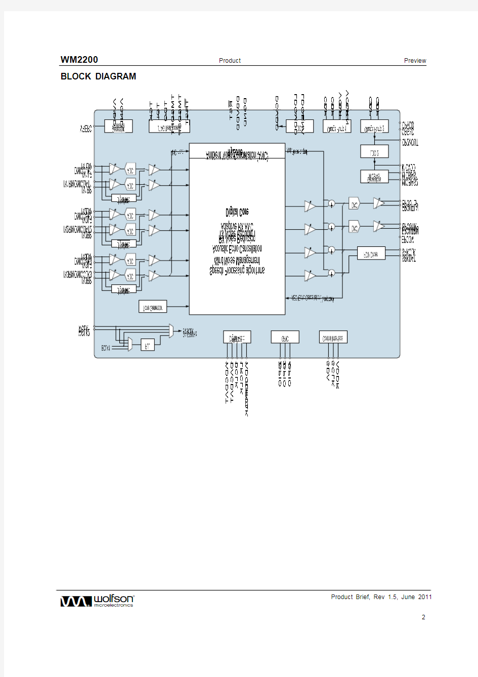
BLOCK DIAGRAM
Product Preview WM2200
TABLE OF CONTENTS
DESCRIPTION (1)
FEATURES (1)
APPLICATIONS (1)
BLOCK DIAGRAM (2)
TABLE OF CONTENTS (3)
USE CASE SCENARIOS EXAMPLES (4)
HANDSET MODE (4)
SPEAKERPHONE MODE (4)
PIN CONFIGURATION (5)
ORDERING INFORMATION (5)
PIN DESCRIPTION (6)
ABSOLUTE MAXIMUM RATINGS (8)
RECOMMENDED OPERATING CONDITIONS (8)
TERMINOLOGY (12)
PACKAGE DIAGRAM (13)
IMPORTANT NOTICE (14)
ADDRESS: (14)
REVISION HISTORY (15)
w Product Brief, Rev 1.5, June 2011
WM2200
Product Preview
w
Product Brief, Rev 1.5, June 2011
USE CASE SCENARIOS EXAMPLES
HANDSET MODE
Speaker Protection
Single Ended
SPEAKERPHONE MODE
Product Preview
WM2200
w
Product Brief, Rev 1.5, June 2011
PIN CONFIGURATION
ORDERING INFORMATION
DEVICE TEMPERATURE
RANGE PACKAGE MOISTURE
SENSITIVITY LEVEL
PEAK SOLDERING TEMPERATURE
WM2200ECS/R -40 to +85o C
90-ball W-CSP (Pb-free)
MSL1 260o C
Note:
Reel quantity = 5000
WM2200
Product Preview
w
Product Brief, Rev 1.5, June 2011
PIN DESCRIPTION
A description of each pin on the WM2200 is provided below.
Note that a table detailing the associated power domain for every input and output pin is provided on the following page. Note that, where multiple pins share a common name, these pins should be tied together on the PCB.
PIN NO NAME TYPE DESCRIPTION
K4 ADCDAT1 Digital Output Audio interface ADC digital audio data K3 ADDR Digital Input 2-wire (I2C) address select
B10, B12, C1, C2, C3, C10, C12, D11
AGND
Supply
Analogue ground (Return path for AVDD)
D2 AVDD
Supply Analogue supply K6 BCLK1
Digital Input / Output Audio interface bit clock
A7 CP1CA
Analogue Output Charge pump 1 fly-back capacitor pin A8 CP1CB
Analogue Output Charge pump 1 fly-back capacitor pin A9 CP1VOUTN
Analogue Output Charge pump 1 positive output decoupling pin B9 CP1VOUTP
Analogue Output Charge pump 1 negative output decoupling pin C7 CP2CA
Analogue Output Charge pump 2 fly-back capacitor pin C8 CP2CB
Analogue Output Charge pump 2 fly-back capacitor pin
C9 CP2VOUT Analogue Output Charge pump 2 output decoupling pin / Supply for LDO2 B7 CPGND Supply Charge pump ground (Return path for CPVDD) B8 CPVDD Supply Supply for Charge Pump 1 and Charge Pump 2 J4 DACDAT1 Digital Input Audio interface DAC digital audio data K12 DBVDD
Supply Digital buffer supply F12 DCVDD Supply Digital core supply / LDO1 output
G12, L2, L4
DGND
Supply
Digital ground (Return path for DBVDD and DCVDD) C11 EPCOM
Analogue Input Earpiece output ground loop noise rejection feedback B11 EPOUTLN
Analogue Output Left earpiece speaker inverted output A10 EPOUTLP
Analogue Output Left earpiece speaker non-inverted output A11 EPOUTRN
Analogue Output Right earpiece speaker inverted output A12 EPOUTRP
Analogue Output Right earpiece speaker non-inverted output
L5 GPIO1/
ADCLRCLK1 Digital Input / Output General Purpose pin GPIO1 / Audio interface ADC left / right clock L8 GPIO2
Digital Input / Output General Purpose pin GPIO2 L7 GPIO3
Digital Input / Output General Purpose pin GPIO3 K7 GPIO4
Digital Input / Output General Purpose pin GPIO4
C5 IN1LN/
DMICCLK1 Analogue Input / Digital Output Left channel single-ended MIC input /
Left channel negative differential MIC input / Digital MIC clock output 1
B5 IN1LP
Analogue Input Left channel line input /
Left channel positive differential MIC input C4 IN1RN/
DMICDAT1 Analogue input / Digital Input Right channel single-ended MIC input /
Right channel negative differential MIC input / Digital MIC data input 1
A5 IN1RP
Analogue Input Right channel line input /
Right channel positive differential MIC input B3 IN2LN/
DMICCLK2 Analogue Input / Digital Output Left channel single-ended MIC input /
Left channel negative differential MIC input / Digital MIC clock output 2
A4 IN2LP
Analogue Input Left channel line input /
Left channel positive differential MIC input
Product Preview
WM2200
w
Product Brief, Rev 1.5, June 2011
PIN NO
NAME
TYPE
DESCRIPTION
A3 IN2RN/
DMICDAT2 Analogue input / Digital Input Right channel single-ended MIC input /
Right channel negative differential MIC input / Digital MIC data input 2
B4 IN2RP
Analogue Input Right channel line input /
Right channel positive differential MIC input B1 IN3LN/
DMICCLK3 Analogue Input / Digital Output Left channel single-ended MIC input /
Left channel negative differential MIC input / Digital MIC clock output 3
B2 IN3LP
Analogue Input Left channel line input /
Left channel positive differential MIC input A1 IN3RN/
DMICDAT3 Analogue input / Digital Input Right channel single-ended MIC input /
Right channel negative differential MIC input / Digital MIC data input 3
A2 IN3RP Analogue Input Right channel line input /
Right channel positive differential MIC input E12 LDOENA Digital Input Enable pin for LDO1 D12 LDOVDD
Supply Supply for LDO1
L6 LRCLK1 Digital Input / Output Audio interface left / right clock K2 MCLK1 Digital Input Master clock 1 K1 MCLK2
Digital Input Master clock 2 B6 MICBIAS1
Analogue Output Microphone bias 1 C6 MICBIAS2
Analogue Output Microphone bias 2
A6 MICVDD Analogue Output LDO2 output decoupling pin (generated internally by WM2200) L1 RST ˉˉˉ
Digital Input
Digital Reset input (active low) J2 SCLK
Digital Input Control interface clock input
L3 SDA
Digital Input / Output Control interface data input and output / acknowledge output L12 SPKCLK
Digital Output Digital speaker (PDM) clock output L11 SPKDAT Digital Output Digital speaker (PDM) data output J12 TCK Digital Input JTAG clock input G11 TDI
Digital Input JTAG data input K11 TDO Digital Output JTAG data output
H11 TMSDFT Digital Input JTAG mode select input (Wolfson only) H12 TMSDSP Digital Input JTAG mode select input
J11 TRST ˉˉˉˉˉ
Digital Input
JTAG Test Access Port reset input (active low, internal pull-down).
This input should be logic 0 for normal WM2200 operation. D1 VREFC Analogue Output Bandgap reference decoupling capacitor connection
E1, E2, E11,
F1, G1, G2, H1, H2, J1, J3, J5, J6, J7, J8, J9, J10, K5, K8, K9, K10, L9,
L10 DNC
Do Not Connect
WM2200
Product Preview
w
Product Brief, Rev 1.5, June 2011
ABSOLUTE MAXIMUM RATINGS
Absolute Maximum Ratings are stress ratings only. Permanent damage to the device may be caused by continuously operating at or beyond these limits. Device functional operating limits and guaranteed performance specifications are given under Electrical
Characteristics at the test conditions specified.
ESD Sensitive Device. This device is manufactured on a CMOS process. It is therefore generically susceptible to damage from excessive static voltages. Proper ESD precautions must be taken during handling and storage of this device.
Wolfson tests its package types according to IPC/JEDEC J-STD-020B for Moisture Sensitivity to determine acceptable storage conditions prior to surface mount assembly. These levels are:
MSL1 = unlimited floor life at <30°C / 85% Relative Humidity. Not normally stored in moisture barrier bag. MSL2 = out of bag storage for 1 year at <30°C / 60% Relative Humidity. Supplied in moisture barrier bag. MSL3 = out of bag storage for 168 hours at <30°C / 60% Relative Humidity. Supplied in moisture barrier bag. The Moisture Sensitivity Level for each package type is specified in Ordering Information.
CONDITION MIN MAX
Supply voltages (DBVDD) -0.3V +4.5V Supply voltages (LDOVDD, AVDD, DCVDD) -0.3V +2.5V Supply voltages (CPVDD) -0.3V +2.2V Voltage range digital inputs DGND - 0.3V DBVDD + 0.3V Voltage range analogue inputs AGND - 0.3V
MICVDD + 0.25V
Operating temperature range, T A -40oC +85oC Operating junction temperature, T J -40oC +125oC Storage temperature after soldering -65oC +150oC
RECOMMENDED OPERATING CONDITIONS
PARAMETER SYMBOL MIN TYP MAX UNIT
Digital supply range (Core) DCVDD 1.14 1.2 1.89 V Digital supply range (I/O)
DBVDD 1.71 1.8 3.6 V LDO supply range
LDOVDD 1.71 1.8 1.89 V Charge Pump supply range CPVDD 1.71 1.8 1.89 V Analogue supply range AVDD 1.71 1.8 1.89 V
Ground DGND, AGND, CPGND 0 V
Product Preview
WM2200
w
Product Brief, Rev 1.5, June 2011
ELECTRICAL CHARACTERISTICS
Test Conditions
DBVDD = LDOVDD = CPVDD = AVDD = 1.8V, DCVDD = 1.2V,
T A = +25o
C, 1kHz signal, fs = 16kHz, PGA gain = 0dB, 24-bit audio data unless otherwise stated.
PARAMETER SYMBOL TEST CONDITIONS MIN TYP MAX UNIT Analogue Inputs (IN1L, IN1R, IN2L, IN2R, IN3L, IN3R) Full-scale input signal level
V INFS Single-ended PGA input 0.5
-6
Vrms
dBV Differential PGA input
1 0 Vrms
dBV Input resistance R IN
All PGA gain settings
10
12
k Ω
Input capacitance
C IN 5 pF Input Programmable Gain Amplifiers (PGAs)
Minimum programmable gain 0 dB Maximum programmable gain 31 dB
Programmable gain step size Guaranteed monotonic
1
dB
Common mode rejection ratio
CMRR
Differential PGA mode,
PGA gain = +30dB 50 60 dB Differential PGA mode,
PGA gain = 0dB
60 70
Analogue Input Paths (INnL, INnR) to ADC Signal to Noise Ratio (A-weighted)
SNR High performance mode (INn_OSR = 1)
95 99 dB
Normal mode (INn_OSR = 0)
92 96 Total Harmonic Distortion THD -1dBFS ADC output -83 -80 dB Total Harmonic Distortion Plus Noise
THD+N
-1dBFS ADC output
-81
-78
dB
Channel separation (Left/Right) 95 100 dB Input path crosstalk 95 100 dB Input noise floor A-weighted, PGA gain = +18dB -110 -105 dBV
PSRR (all supplies) PSRR
100mV (peak-peak) 217Hz 80 dB
100mV(peak-peak) 10kHz
70
ADC Digital Filters Passband +/- 0.05dB 0 0.454 fs -6dB 0.5 fs
Passband ripple +/- 0.05 dB Stopband
0.546 fs Stopband attenuation
f > 0.546 fs
-85
dB
Group delay
2 ms
WM2200
Product Preview
w
Product Brief, Rev 1.5, June 2011
Test Conditions
DBVDD = LDOVDD = CPVDD = AVDD = 1.8V, DCVDD = 1.2V,
T A = +25o C, 1kHz signal, fs = 16kHz, PGA gain = 0dB, 24-bit audio data unless otherwise stated.
PARAMETER SYMBOL TEST CONDITIONS MIN TYP MAX UNIT DAC Digital Filters Passband +/- 0.05dB 0 0.454 fs -6dB 0.5 fs
Passband ripple +/- 0.05 dB Stopband
0.546 fs Stopband attenuation
f > 0.546 fs
-85
dB
Group delay
1.5 ms Earpiece Output Programmable Gain Amplifiers (PGAs)
Minimum programmable gain -6 dB Maximum programmable gain +6 dB
Programmable gain step size
Guaranteed monotonic
1
dB
DAC to Earpiece Output (EPOUTLP+EPOUTLN, EPOUTRP+EPOUTRN, R L = 32Ω BTL)
Maximum output power P O 0.1% THD 60 mW
10% THD
125 Signal to Noise Ratio SNR A-weighted 96 100 dB
Total Harmonic Distortion THD P O = 50mW -71 -68 dB Total Harmonic Distortion Plus Noise
THD+N P O = 50mW -69 -66 dB Total Harmonic Distortion THD P O = 5mW -77 -74 dB Total Harmonic Distortion Plus Noise
THD+N P O = 5mW
-75
-72
dB
Channel separation (Left/Right) 80 dB Output noise floor A-weighted, PGA gain = -3dB -106 -105 dBV
PSRR (AVDD, CPVDD) PSRR
100mV (peak-peak) 217Hz 70 80 dB
100mV (peak-peak) 10kHz
60
65
DC offset at Load 0.2 0.5 mV DAC to Earpiece Output (EPOUTLP+EPOUTLN, EPOUTRP+EPOUTRN, R L = 16Ω BTL)
Maximum output power P O 0.1% THD 60 mW
10% THD
125 Signal to Noise Ratio SNR A-weighted 98 102 dB
Total Harmonic Distortion THD P O = 100mW -71 -68 dB Total Harmonic Distortion Plus Noise
THD+N P O = 100mW -69 -66 dB Total Harmonic Distortion THD P O = 5mW -77 -74 dB Total Harmonic Distortion Plus Noise
THD+N P O = 5mW
-75 -72 dB Channel separation (Left/Right)
1kHz full scale signal
80
dB
Output noise floor A-weighted PGA gain = -6dB -108 -105 dBV
PSRR (AVDD, CPVDD) PSRR
100mV (peak-peak) 217Hz 70 80 dB
100mV (peak-peak) 10kHz
60
65
DC offset at Load 0.2 0.5 mV Earpiece Output Driver (EPOUTLP+EPOUTLN, EPOUTRP+EPOUTRN)
Earpiece load resistance 15 ?
Earpiece load capacitance
200 pF
Product Preview
WM2200
w
Product Brief, Rev 1.5, June 2011
Test Conditions
DBVDD = LDOVDD = CPVDD = AVDD = 1.8V, DCVDD = 1.2V,
T A = +25o C, 1kHz signal, fs = 16kHz, PGA gain = 0dB, 24-bit audio data unless otherwise stated.
PARAMETER SYMBOL TEST CONDITIONS MIN TYP MAX UNIT MICVDD Regulator (LDO2) Output voltage
V MICVDD
1.7V to
2.8V
in 50mV steps
V
Start-up time
4.7μF on MICVDD
1.5 ms
Microphone Bias (MICBIAS1, MICBIAS2)
Bias voltage Regulator mode (MICBn_MODE=0) 1.0mA load current
Note that MICVDD must be at least 200mV higher than V MICBIAS
V MICBIAS MICBn_LVL =000 -5% 1.5 +5% V
MICBn_LVL =
001 -5% 1.8 +5%
MICBn_LVL =
010 -5% 1.9 +5% MICBn_LVL =011 -5% 2.0 +5% MICBn_LVL =100 -5% 2.2 +5% MICBn_LVL =101 -5% 2.4 +5% MICBn_LVL =
110 -5% 2.5 +5% MICBn_LVL =111 -5% 2.6 +5%
Bias voltage
Switch mode (MICBn_MODE=1) 5.0mA load current V MICBIAS MICVDD - 80mV
MICVDD V
Maximum output current
Regulator mode (MICBn_MODE=0), V MICVDD - V MICBIAS >200mV
2.4 mA Switch mode (MICBn_MODE=1)
3.6 Output noise spectral density 1kHz to 20kHz 100 nV/√Hz Integrated noise voltage (A-weighted)
Regulator mode (MICBn_MODE=0), 100Hz to 7kHz 5 μVrms Power Supply Rejection Ratio (AVDD, CPVDD)
PSRR
100mV (peak-peak) 217Hz 100 dB
100mV (peak-peak) 10kHz
80
Frequency Locked Loop (FLL) Input Frequency
F REF FLL_CLK_REF_DIV =
00 0.032
13.5 MHz FLL_CLK_REF_DIV = 01 0.064 27 FLL_CLK_REF_DIV = 10
0.128
36.864
Lock Time
F REF = 32kHz,
F OUT = 24.576MHz 2.5 ms F REF = 12MHHz, F OUT = 24.576MHz
0.3
WM2200
Product Preview
w
Product Brief, Rev 1.5, June 2011
Test Conditions
DBVDD = LDOVDD = CPVDD = AVDD = 1.8V, DCVDD = 1.2V,
T A = +25o C, 1kHz signal, fs = 16kHz, PGA gain = 0dB, 24-bit audio data unless otherwise stated.
PARAMETER SYMBOL TEST CONDITIONS MIN TYP MAX UNIT Digital Input / Output (except DMICDATn and DMICCLKn) Input HIGH Level
V IH DBVDD =
1.8V 0.65 × DBVDD
V
DBVDD = 3.3V 0.7 × DBVDD
Input LOW Level
V IL DBVDD = 1.8V 0.35 × DBVDD
V
DBVDD =
3.3V 0.3 ×
DBVDD
Note that digital input pins should not be left unconnected or floating. Output HIGH Level V OH I OL = 1mA 0.9 × DBVDD
V Output LOW Level V OL
I OH = -1mA
0.1 ×
DBVDD
V
Input capacitance
10 pF
Input leakage
-1 1 μA
Digital Microphone Input / Output (DMICDATn and DMICCLKn)
DMICDATn and DMICCLKn are each referenced to a selectable supply, V SUP , according to the INn_DMIC_SUP registers DMICDATn input HIGH Level V IH 0.65 × V SUP V DMICDATn input LOW Level V IL 0.35 × V SUP V DMICCLKn output HIGH Level V OH I OL = 1mA
0.8 × V SUP
V
DMICCLKn output LOW Level V OL
I OH = -1mA 0.2 × V SUP V
Input capacitance 10 pF
Input leakage -1 1 μA
TERMINOLOGY
1. Signal-to-Noise Ratio (dB) – SNR is a measure of the difference in level between the maximum full scale output
signal and the output with no input signal applied. 2. Total Harmonic Distortion (dB) – THD is the level of the rms value of the sum of harmonic distortion products relative to the amplitude of the measured output signal.
3. Total Harmonic Distortion plus Noise (dB) – THD+N is the level of the rms value of the sum of harmonic distortion products plus noise in the specified bandwidth relative to the amplitude of the measured output signal.
4.
Crosstalk (L/R) (dB) – left-to-right and right-to-left channel crosstalk is the measured signal level in the idle channel at the test signal frequency relative to the signal level at the output of the active channel. The active channel is configured and supplied with an appropriate input signal to drive a full scale output, with signal measured at the output of the associated idle channel.
5.
Multi-Path Channel Separation (dB) – is the measured signal level in the idle path at the test signal frequency relative to the signal level at the output of the active path. The active path is configured and supplied with an appropriate input signal to drive a full scale output, with signal measured at the output of the specified idle path.
6. Mute Attenuation – This is a measure of the difference in level between the full scale output signal and the output with mute applied.
7.
All performance measurements carried out with 20kHz low pass filter, and where noted an A-weighted filter. Failure to use such a filter will result in higher THD and lower SNR readings than are found in the Electrical Characteristics. The low pass filter removes out of band noise; although it is not audible it may affect dynamic specification values.
Product Preview
WM2200
w
Product Brief, Rev 1.5, June 2011
PACKAGE DIAGRAM
NOTES:
1. PRIMARY DATUM -Z-AND SEATING PLANE ARE DEFINED BY THE SPHERICAL CROWNS OF THE SOLDER BALLS.
2. THIS DIMENSION INCLUDES STAND-OFF HEIGHT ‘A1’, SILICON THICKNESS AND BACKSIDE COATING.
3. A1 CORNER IS IDENTIFIED BY INK/LASER MARK ON TOP PACKAGE.
4. BILATERAL TOLERANCE ZONE IS APPLIED TO EACH SIDE OF THE PACKAGE BODY.
5. ‘e’ REPRESENTS THE BASIC SOLDER BALL GRID PITCH.
6. THIS DRAWING IS SUBJECT TO CHANGE WITHOUT NOTICE.
7. FOLLOWS JEDEC DESIGN GUIDE MO-211-C.
8. f1 = NOMINAL DISTANCE OF BALL CENTRE TO DIE EDGE X AXIS (AS PER POD) –APPLICABLE TO ALL CORNERS OF DIE.9. f2 = NOMINAL DISTANCE OF DIE CENTRE TO DIE EDGE IN Y AXIS (AS PER POD) –APPLICABLE TO ALL CORNERS OF DIE.
A10.191D D1E E1e 4.400 BSC 4.7174.000 BSC 0.400 BSC 5.034Dimensions (mm)Symbols
MIN NOM MAX NOTE
A 0.603A20.3680.380
0.3925f10.6160.5900.1980.205
g 0.025h
0.270
f20.3170.358589
5.0144.697
5.0544.73744
WM2200Product Preview IMPORTANT NOTICE
Wolfson Microelectronics plc (“Wolfson”) products and services are sold subject to Wolfson’s terms and conditions of sale, delivery and payment supplied at the time of order acknowledgement.
Wolfson warrants performance of its products to the specifications in effect at the date of shipment. Wolfson reserves the
right to make changes to its products and specifications or to discontinue any product or service without notice. Customers
should therefore obtain the latest version of relevant information from Wolfson to verify that the information is current.
Testing and other quality control techniques are utilised to the extent Wolfson deems necessary to support its warranty. Specific testing of all parameters of each device is not necessarily performed unless required by law or regulation.
In order to minimise risks associated with customer applications, the customer must use adequate design and operating safeguards to minimise inherent or procedural hazards. Wolfson is not liable for applications assistance or customer product design. The customer is solely responsible for its selection and use of Wolfson products. Wolfson is not liable for
such selection or use nor for use of any circuitry other than circuitry entirely embodied in a Wolfson product.
Wolfson’s products are not intended for use in life support systems, appliances, nuclear systems or systems where malfunction can reasonably be expected to result in personal injury, death or severe property or environmental damage.
Any use of products by the customer for such purposes is at the customer’s own risk.
Wolfson does not grant any licence (express or implied) under any patent right, copyright, mask work right or other intellectual property right of Wolfson covering or relating to any combination, machine, or process in which its products or services might be or are used. Any provision or publication of any third party’s products or services does not constitute Wolfson’s approval, licence, warranty or endorsement thereof. Any third party trade marks contained in this document belong to the respective third party owner.
Reproduction of information from Wolfson datasheets is permissible only if reproduction is without alteration and is accompanied by all associated copyright, proprietary and other notices (including this notice) and conditions. Wolfson is
not liable for any unauthorised alteration of such information or for any reliance placed thereon.
Any representations made, warranties given, and/or liabilities accepted by any person which differ from those contained in
this datasheet or in Wolfson’s standard terms and conditions of sale, delivery and payment are made, given and/or accepted at that person’s own risk. Wolfson is not liable for any such representations, warranties or liabilities or for any reliance placed thereon by any person.
ADDRESS:
Wolfson Microelectronics plc
Westfield House
26 Westfield Road
Edinburgh
EH11 2QB
Tel :: +44 (0)131 272 7000
Fax :: +44 (0)131 272 7001
Email :: sales@https://www.360docs.net/doc/2111328549.html,
w Product Brief, Rev 1.5, June 2011
Product Preview WM2200 REVISION HISTORY
DATE REV ORIGINATOR CHANGES
31/01/11 1.3 JMacD Removed ‘Confidential from headers and footers
Table of Contents added
Ordering Information added
14/04/11 1.4 JMacD Package diagram inserted
14/04/11 1.4 PH Description, Features, Block diagram & Electrical Characteristics updated,
consistent with datasheet
Pin configuration and Pin descriptions added
02/06/11 1.5 JMacD Description and Features updated to be consistent with datasheet release, Rev
1.0
w Product Brief, Rev 1.5, June 2011