MSA-0505中文资料
Cascadable Silicon Bipolar MMIC?Amplifier Technical Data
Features
?Cascadable 50 ? Gain Block ?High Output Power:18.0 dBm Typical P 1 dB at 1.0?GHz ?Low Distortion:
29.0 dBm Typical I P 3 at 1.0?GHz ?7.0 dB Typical Gain at 1.0?GHz ?Surface Mount Plastic Package ?Tape-and-Reel Packaging Option Available [1]
MSA-0505
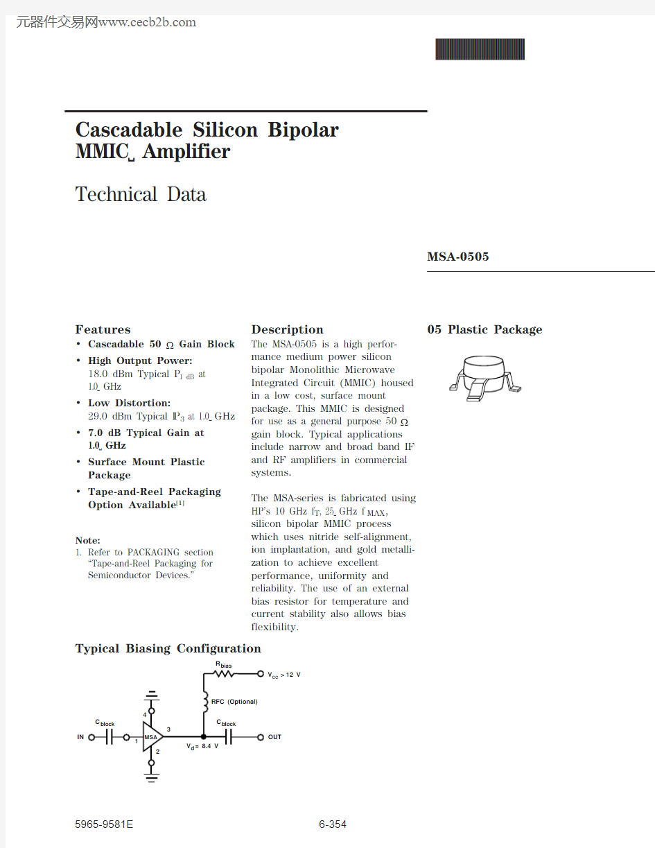
05 Plastic Package
Description
The MSA-0505 is a high perfor-mance medium power silicon bipolar Monolithic Microwave Integrated Circuit (MMIC) housed in a low cost, surface mount package. This MMIC is designed for use as a general purpose 50 ?gain block. Typical applications include narrow and broad band IF and RF amplifiers in commercial systems.
The MSA-series is fabricated using HP’s 10 GHz f T , 25?GHz f MAX ,silicon bipolar MMIC process which uses nitride self-alignment,ion implantation, and gold metalli-zation to achieve excellent performance, uniformity and reliability. The use of an external bias resistor for temperature and current stability also allows bias flexibility.
Typical Biasing Configuration
R
V CC > 12 V
IN
OUT
Note:
1.Refer to PACKAGING section “Tape-and-Reel Packaging for Semiconductor Devices.”
MSA-0505 Absolute Maximum Ratings
Parameter Absolute Maximum [1]
Device Current
135 mA Power Dissipation [2,3] 1.5 W RF Input Power
+25 dBm Junction Temperature 200°C Storage Temperature
–65 to 150°C
Thermal Resistance [2,4]:
θjc = 85°C/W
Notes:
1.Permanent damage may occur if any of these limits are exceeded.
2.T CASE = 25°C.
3.Derate at 11.8 mW/°C for T C > 73°C.
4.See MEASUREMENTS section “Thermal Resistance” for more information.
P 1 dB Output Power at 1 dB Gain Compression f = 0.5 GHz dBm 19.0f = 1.0 GHz dBm 16.018.0G P Power Gain (|S 21|2) f = 0.5 GHz dB
7.5f = 1.0 GHz 6.0
7.0?G P Gain Flatness f = 0.1 to 1.5 GHz
dB ±0.75f 3 dB 3 dB Bandwidth [2]GHz
2.3I nput VSWR f = 0.1 to 1.5 GHz 1.6:1Output VSWR
f = 0.1 to 1.5 GHz 2.0:1
I P 3Third Order Intercept Point f = 1.0 GHz dBm 29.0NF 50 ? Noise Figure f = 1.0 GHz dB 6.5t D Group Delay f = 1.0 GHz psec 190V d Device Voltage
V 6.7
8.410.1
dV/dT
Device Voltage Temperature Coefficient
mV/°C
–16.0
Notes:
1.The recommended operating current range for this device is 60 to 100 mA. Typical performance as a function of current is on the following page.
2.Referenced from 0.1 GHz Gain (G P ).
Electrical Specifications [1], T A = 25°C
Symbol
Parameters and Test Conditions: I d = 80 mA, Z O = 50 ?
Units
Min.
Typ.
Max.
VSWR Part Number Ordering Information
Part Number No. of Devices
Container MSA-0505-TR15007" Reel MSA-0505-STR
10
Strip
For more information, see “Tape and Reel Packaging for Semiconductor Devices”.
MSA-0505 Typical Scattering Parameters (T A = 25°C, I d = 80 mA)
Freq.MHz
Mag
Ang
dB
Mag
Ang
dB
Mag
Ang
Mag
Ang
k
5.56–3914.9 5.56161–18.5.12039.65–360.6025.24–1039.7 3.05156–13.9.20212.25–900.9750.15–1308.2 2.57163–13.7.2077.15–116 1.15100.13–155
7.8 2.45165–13.7.2073.11–132 1.21200.12–1707.7 3.43161–13.5.2111.11–145 1.21400.121787.5 2.37148–13.6.209–1.14–146 1.23600.131727.4 2.34134–13.6.209–2.17–151 1.23800.13
1687.2 2.29119–13.6.209–3.21–157 1.231000.141667.0 2.24105–13.4.213–4.25–164 1.211500.21159 6.4 2.0972–13.3.217–6.34176 1.162000.30148 5.2 1.8242–13.1.222–9.42159 1.122500.40136 4.1 1.6017–12.9.227–11.48146 1.053000.52121 2.7 1.36–7–12.6.234–16.551330.92
A model for this device is available in the DEVICE MODELS section.
S 11S 21S 12 S 22
Typical Performance, T A = 25°C
(unless otherwise noted)
2
4
6810
810121416182022
24
POWER OUT (dBm)Figure 1. Typical Gain vs. Power Out,T A = 25°C, I d
= 80 mA.
G A I N (d B )
FREQUENCY (GHz)
Figure 2. Device Current vs. Voltage.
30
60
90
120
V d (V)
I d (m A )
3
69
12
1214
18
16
22
20
P 1 d B (d B m )
TEMPERATURE (°C)
Figure 3. Output Power at 1 dB Gain Compression, vs. Case Temperature, I d = 80 mA.
18
–25
+25
+85
1434
P 1 d B (d B m )
I d (mA)
Figure 5. Output Power at 1 dB Gain Compression, Third Order Intercept vs. Case Temperature, f = 1.0 GHz.
Figure 4. Gain vs. Frequency,I d = 80 to 100 mA.
60
708090100
I P 3 (d B m )
0.5 GHz
1.0 GHz
2.0 GHz
.01
.05
0.1
0.5 1.0
5.0
14
121086420G p (d B )
05 Plastic Package Dimensions
(4 PLCS)
0.0005 ± 0.010 (0.013 ± 0.25)
DIA Notes:
(unless otherwise specified)1. Dimensions are in
2. Tolerances
in .xxx = ± 0.005 mm .xx = ± 0.13
mm