1SMB5913BT3
1SMB5913BT3 Series
Preferred Device
3 Watt Plastic
Surface Mount
Zener Voltage Regulators
This complete new line of 3 Watt Zener diodes offers the following advantages.
Features
?Zener V oltage Range ? 3.3 V to 200 V
?ESD Rating of Class 3 (>16 kV) per Human Body Model ?Flat Handling Surface for Accurate Placement ?Package Design for Top Side or Bottom Circuit Board Mounting ?Pb?Free Packages are Available
Mechanical Characteristics:
CASE:V oid-free, transfer-molded plastic
FINISH:All external surfaces are corrosion resistant and leads are readily solderable
MAXIMUM LEAD TEMPERATURE FOR SOLDERING PURPOSES: 260°C for 10 Seconds
LEADS:Modified L?Bend providing more contact area to bond pads POLARITY:Cathode indicated by polarity band FLAMMABILITY RATING:UL 94 V?0
MAXIMUM RATINGS
Rating Symbol Value Unit Maximum Steady State Power
Dissipation @ T L = 75°C
Measured at Zero Lead Length
Derate Above 75°C
Thermal Resistance from Junction?to?Lead
P D
R q JL
3.0
40
25
W
mW/°C
°
C/W
Maximum Steady State Power Dissipation
@ T A = 25°C (Note )
Derate Above 25°C
Thermal Resistance from Junction?to?Ambient
P D
R q JA
550
4.4
226
mW
mW/°C
°C/W
Operating and Storage Temperature Range T J, T stg?65 to
+150
°C
Stresses exceeding Maximum Ratings may damage the device. Maximum Ratings are stress ratings only. Functional operation above the Recommended Operating Conditions is not implied. Extended exposure to stresses above the Recommended Operating Conditions may affect device reliability.
1.FR?4 board, using recommended footprint.
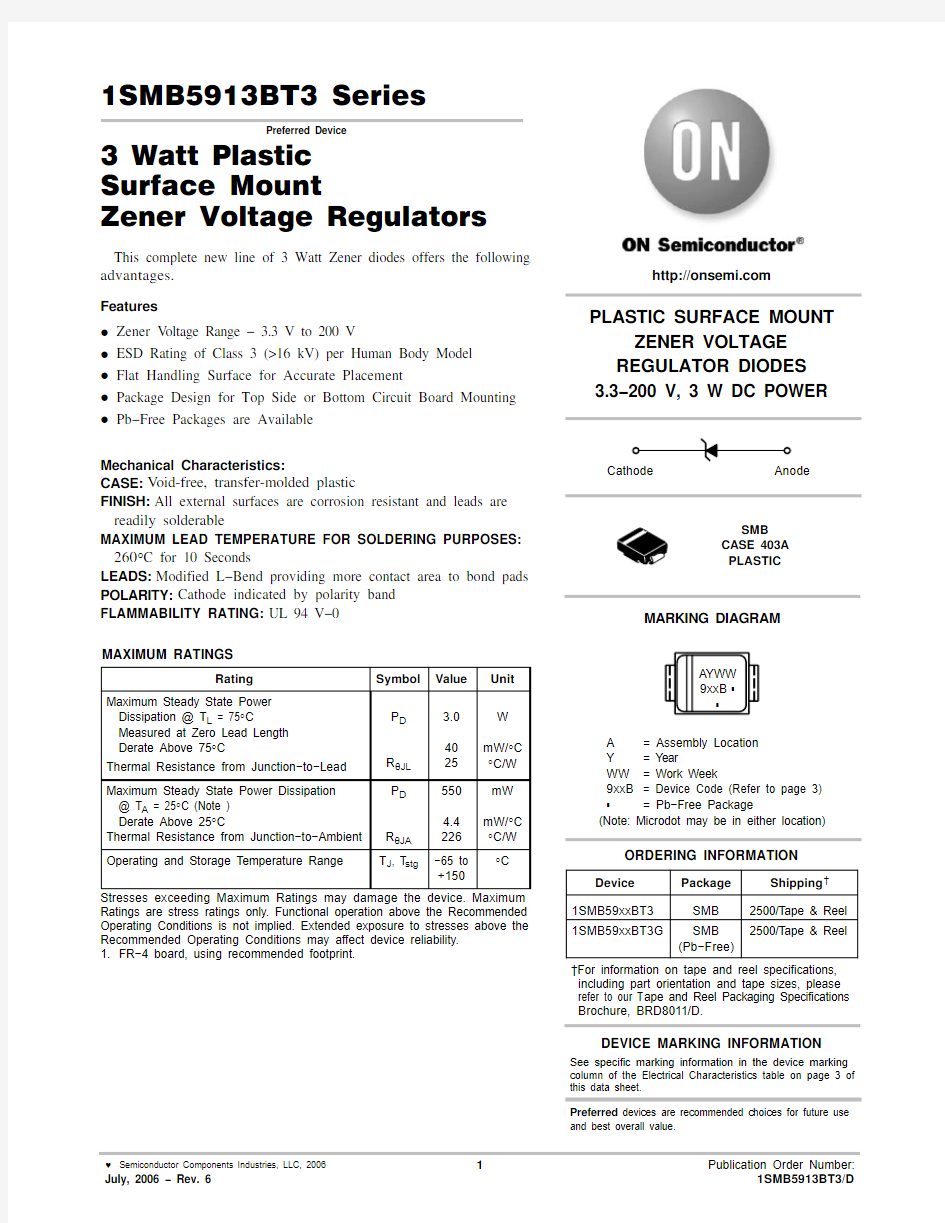
PLASTIC SURFACE MOUNT
ZENER VOLTAGE
REGULATOR DIODES
3.3?200 V, 3 W DC POWER
SMB
CASE 403A
PLASTIC
Cathode Anode
MARKING DIAGRAM
https://www.360docs.net/doc/309639555.html,
Device Package Shipping?
ORDERING INFORMATION
1SMB59xxBT3SMB2500/Tape & Reel 1SMB59xxBT3G SMB
(Pb?Free)
2500/Tape & Reel
?For information on tape and reel specifications, including part orientation and tape sizes, please refer to our T ape and Reel Packaging Specifications Brochure, BRD8011/D.
Preferred devices are recommended choices for future use and best overall value.
A= Assembly Location
Y= Year
WW= Work Week
9xxB= Device Code (Refer to page 3)
G= Pb?Free Package
AYWW
9xxB G
G
See specific marking information in the device marking column of the Electrical Characteristics table on page 3 of this data sheet.
DEVICE MARKING INFORMATION
(Note: Microdot may be in either location)
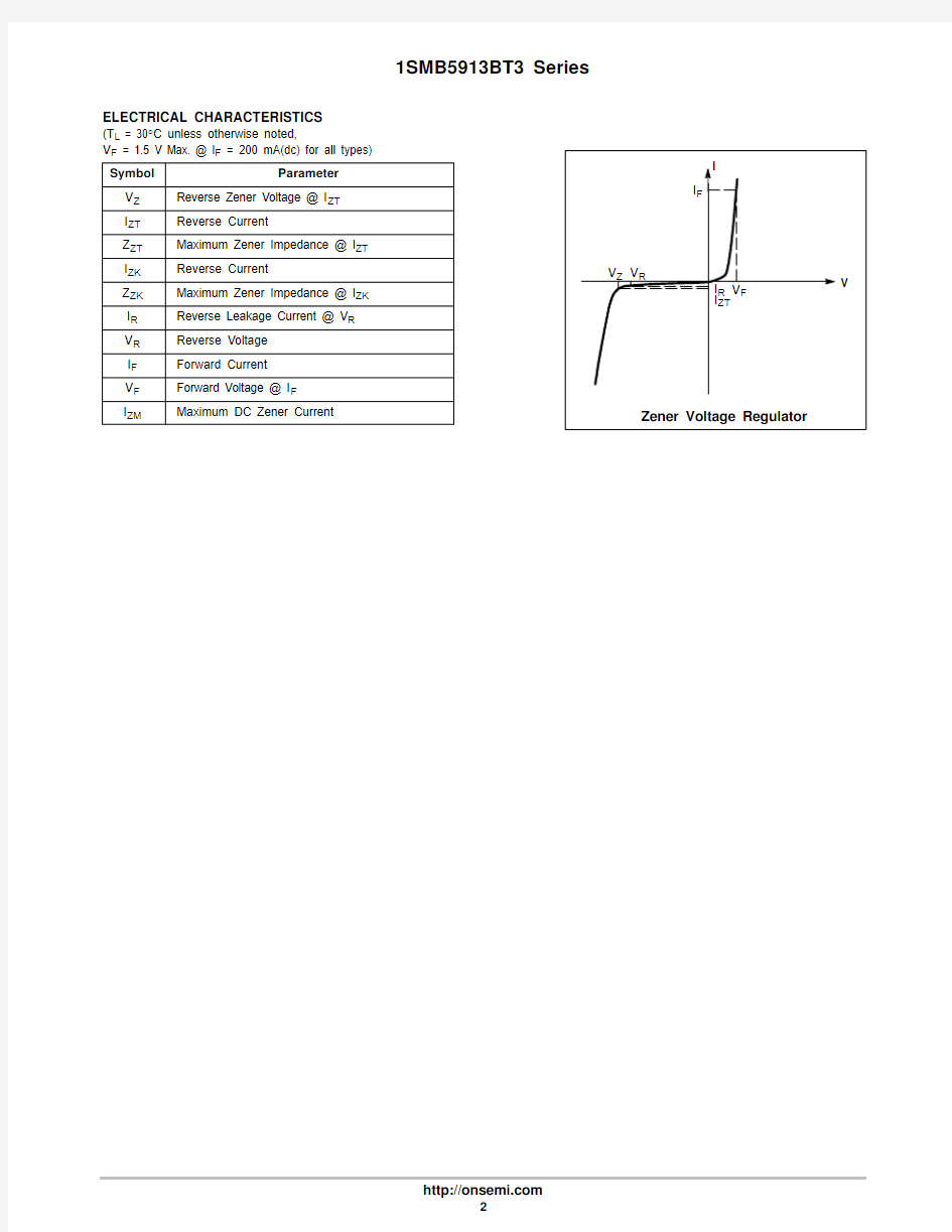
ELECTRICAL CHARACTERISTICS
(T L = 30°C unless otherwise noted,
V F = 1.5 V Max. @ I F = 200 mA(dc) for all types) Array Symbol Parameter V Z Reverse Zener Voltage @ I ZT
I ZT Reverse Current
Z ZT Maximum Zener Impedance @ I ZT
I ZK Reverse Current
Z ZK Maximum Zener Impedance @ I ZK
I R Reverse Leakage Current @ V R
V R Reverse Voltage
I F Forward Current
V F Forward Voltage @ I F
I ZM Maximum DC Zener Current
ELECTRICAL CHARACTERISTICS (Devices listed in bold, italic are ON Semiconductor Preferred devices.) (T L = 30°C unless otherwise noted, V F = 1.5 V Max. @ I F = 200 mA(dc) for all types)
Device* (Note 2)
Device
Marking
Zener Voltage (Note 3)Zener Impedance (Note 4)Leakage Current
I ZM
V Z(Volts)@ I ZT Z ZT@ I ZT Z ZK@ I ZK I R@ V R
Min Nom Max mA W W mA m A Volts mA(dc)
1SMB5913BT3, G913B 3.13 3.3 3.47113.61050011001454 1SMB5914BT3, G914B 3.42 3.6 3.78104.295001751416 1SMB5915BT3, G915B 3.70 3.9 4.1096.17.55001251384 1SMB5916BT3, G916B 4.08 4.3 4.5287.26500151348
1SMB5917BT3, G917B 4.46 4.7 4.9479.8550015 1.5319 1SMB5918BT3, G918B 4.84 5.1 5.3673.54350152294 1SMB5919BT3, G919B 5.32 5.6 5.8866.92250153267 1SMB5920BT3, G920B 5.89 6.2 6.5160.52200154241
1SMB5921BT3, G921B 6.46 6.87.1455.1 2.520015 5.2220 1SMB5922BT3, G922B7.127.57.885034000.556200 1SMB5923BT3, G923B7.798.28.6145.7 3.54000.55 6.5182 1SMB5924BT3, G924B8.649.19.5641.245000.557164 1SMB5925BT3, G925B9.51010.537.5 4.55000.2558150 1SMB5926BT3, G926B10.451111.5534.1 5.55500.2518.4136 1SMB5927BT3, G927B11.41212.631.2 6.55500.2519.1125 1SMB5928BT3, G928B12.351313.6528.875500.2519.9115
1SMB5929BT3, G929B14.251515.752596000.25111.4100 1SMB5930BT3, G930B15.21616.823.4106000.25112.293 1SMB5931BT3, G931B17.11818.920.8126500.25113.783 1SMB5932BT3, G932B19202118.7146500.25115.275 1SMB5933BT3, G933B20.92223.11717.56500.25116.768 1SMB5934BT3, G934B22.82425.215.6197000.25118.262 1SMB5935BT3, G935B25.652728.3513.9237000.25120.655 1SMB5936BT3, G936B28.53031.512.5287500.25122.850
1SMB5937BT3, G937B31.353334.6511.4338000.25125.145 1SMB5938BT3, G938B34.23637.810.4388500.25127.441 1SMB5939BT3, G939B37.053940.959.6459000.25129.738 1SMB5940BT3, G940B40.854345.158.7539500.25132.734 1SMB5941BT3, G941B44.654749.3586710000.25135.831 1SMB5942BT3, G942B48.455153.557.37011000.25138.829 1SMB5943BT3, G943B53.25658.8 6.78613000.25142.626 1SMB5944BT3, G944B58.96265.1610015000.25147.124
1SMB5945BT3, G945B64.66871.4 5.512017000.25151.722 1SMB5946BT3, G946B71.257578.75514020000.2515620 1SMB5947BT3, G947B77.98286.1 4.616025000.25162.218 1SMB5948BT3, G948B86.459195.55 4.120030000.25169.216 1SMB5949BT3, G949B95100105 3.725031000.2517615 1SMB5950BT3, G950B104.5110115.5 3.430040000.25183.613 1SMB5951BT3, G951B114120126 3.138045000.25191.212 1SMB5952BT3, G952B123.5130136.5 2.945050000.25198.811
1SMB5953BT3, G953B142.5150157.5 2.560060000.25111410 1SMB5954BT3, G954B152160168 2.370065000.251121.69 1SMB5955BT3, G955B171180189 2.190070000.251136.88 1SMB5956BT3, G956B190200210 1.9120080000.2511527
2.TOLERANCE AND TYPE NUMBER DESIGNATION The type numbers listed indicate a tolerance of ±5%.
3.ZENER VOLTAGE (V Z) MEASUREMENT
Nominal Zener voltage is measured with the device junction in thermal equilibrium with ambient temperature at 25°C.
4.ZENER IMPEDANCE (Z Z) DERIVATION Z ZT and Z ZK are measured by dividing the ac voltage drop across the device by the ac current
applied. The specified limits are for I Z(ac) = 0.1 I Z(dc) with the ac frequency = 60 Hz.
*The “G” suffix indicates Pb?Free package available.
Figure 1. Steady State Power Derating
0255075100125150
6
5
4
3
2
T, TEMPERATURE (°C)
P
,
M
A
X
I
M
U
M
P
O
W
E
R
D
I
S
S
I
P
A
T
I
O
N
(
W
A
T
T
S
)
D
10
20
30
50
100
200
300
500
PW, PULSE WIDTH (ms)
P
,
P
E
A
K
S
U
R
G
E
P
O
W
E
R
(
W
A
T
T
S
)
P
K
Figure 2. Maximum Surge Power Figure 3. Zener Voltage ? To 12 Volts
10
8
6
4
2
?2
?4
V Z, ZENER VOLTAGE (VOLTS)
,
T
E
M
P
E
R
A
T
U
R
E
C
O
E
F
F
I
C
I
E
N
T
(
m
V
/
C
)
°
θ
V
Z
012345678910
100
50
30
20
10
1
0.5
0.3
0.2
0.1
V Z, ZENER VOLTAGE (VOLTS)
2
5
3
0102030405060708090100
V Z, ZENER VOLTAGE (VOLTS)
100
50
30
20
10
1
0.5
0.3
0.2
0.1
2
5
3
1
T L
T A
Figure 4. Zener Voltage ? 14 To 200 Volts
200
100
70
50
30
20
10
1020305070100200
V Z, ZENER VOLTAGE (VOLTS)
,
T
E
M
P
E
R
A
T
U
R
E
C
O
E
F
F
I
C
I
E
N
T
(
m
V
/
C
)
°
θ
V
Z
Figure 5. V Z = 3.3 thru 10 Volts Figure 6. V Z = 12 thru 82 Volts
I
Z
T
,
R
E
V
E
R
S
E
C
U
R
R
E
N
T
(
m
A
)
I
Z
T
,
R
E
V
E
R
S
E
C
U
R
R
E
N
T
(
m
A
)
Figure 7. Effect of Zener Voltage
V Z , ZENER VOLTAGE (VOLTS)
5
7
10
203050
70
100
200100
Z , D Y N A M I C I M P E D A N C E (O H M S )Z Figure 8. Effect of Zener Current
I Z , ZENER TEST CURRENT (mA)
500200*********Z , D Y N A M I C I M P E D A N C E (O H M S )
Z Rating and Typical Characteristic Curves (T A = 25°C)
PACKAGE DIMENSIONS
SMB
CASE 403A?03
ISSUE E
*For additional information on our Pb?Free strategy and soldering
details, please download the ON Semiconductor Soldering and Mounting Techniques Reference Manual, SOLDERRM/D.
SOLDERING FOOTPRINT*
ǒmm inches
ǔSCALE 8:1
NOTES:
1.DIMENSIONING AND TOLERANCING PER ANSI Y14.5M, 198
2.2.CONTROLLING DIMENSION: INCH.
3.D DIMENSION SHALL BE MEASURED WITHIN DIMENSION P.
DIM A MIN NOM MAX MIN MILLIMETERS
1.90
2.13 2.410.075INCHES A10.050.100.150.002b 1.96 2.03 2.110.077c 0.150.230.300.006
3.30 3.56 3.810.130E
4.06 4.32 4.570.160L 0.76
1.02 1.270.030
0.0840.0950.0040.0060.0800.0830.0090.0120.1400.1500.1700.1800.0400.050
NOM MAX 5.21 5.44 5.590.2050.2140.220H E 0.51 REF
0.020 REF
D L1
ON Semiconductor and are registered trademarks of Semiconductor Components Industries, LLC (SCILLC). SCILLC reserves the right to make changes without further notice to any products herein. SCILLC makes no warranty, representation or guarantee regarding the suitability of its products for any particular purpose, nor does SCILLC assume any liability arising out of the application or use of any product or circuit, and specifically disclaims any and all liability, including without limitation special, consequential or incidental damages.“Typical” parameters which may be provided in SCILLC data sheets and/or specifications can and do vary in different applications and actual performance may vary over time. All operating parameters, including “Typicals” must be validated for each customer application by customer’s technical experts. SCILLC does not convey any license under its patent rights nor the rights of others. SCILLC products are not designed, intended, or authorized for use as components in systems intended for surgical implant into the body, or other applications intended to support or sustain life, or for any other application in which the failure of the SCILLC product could create a situation where personal injury or death may occur. Should Buyer purchase or use SCILLC products for any such unintended or unauthorized application, Buyer shall indemnify and hold SCILLC and its officers, employees, subsidiaries, affiliates,and distributors harmless against all claims, costs, damages, and expenses, and reasonable attorney fees arising out of, directly or indirectly, any claim of personal injury or death associated with such unintended or unauthorized use, even if such claim alleges that SCILLC was negligent regarding the design or manufacture of the part. SCILLC is an Equal Opportunity/Affirmative Action Employer. This literature is subject to all applicable copyright laws and is not for resale in any manner.
PUBLICATION ORDERING INFORMATION