AD7193

4-Channel, 4.8 kHz, Ultralow Noise, 24-Bit Sigma-Delta ADC with PGA
Data Sheet
AD7193
Rev. C
Information furnished by Analog Devices is believed to be accurate and reliable. However , no responsibility is assumed by Analog Devices for its use, nor for any infringements of patents or other rights of third parties that may result from its use. Specifications subject to change without notice. No license is granted by implication or otherwise under any patent or patent rights of Analog Devices. T rademarks and registered trademarks are the property of their respective owners.
One Technology Way, P.O. Box 9106, Norwood, MA 02062-9106, U.S.A. Tel: 781.329.4700 https://www.360docs.net/doc/4175623.html, Fax: 781.461.3113 ?2009–2011 Analog Devices, Inc. All rights reserved.
FEATURES
Fast settling filter option
4 differential/8 pseudo differential input channels RMS noise: 11 nV @ 4.7 Hz (gain = 128) 15.
5 noise-free bits @ 2.4 kHz (gain = 128) Up to 22 noise-free bits (gain = 1) Offset drift: ±5 nV/°C Gain drift: ±1 ppm/°C Specified drift over time
Automatic channel sequencer Programmable gain (1 to 128) Output data rate: 4.7 Hz to 4.8 kHz Internal or external clock
Simultaneous 50 Hz/60 Hz rejection 4 general-purpose digital outputs Power supply
AV DD : 3 V to 5.25 V DV DD : 2.7 V to 5.25 V Current: 4.65 mA
Temperature range: ?40°C to +105°C
28-lead TSSOP and 32-lead LFCSP packages Interface
3-wire serial
SPI, QSPI?, MICROWIRE?, and DSP compatible Schmitt trigger on SCLK
APPLICATIONS
PLC/DCS analog input modules Data acquisition
Strain gage transducers
Pressure measurement Temperature measurement Flow measurement Weigh scales Chromatography
Medical and scientific instrumentation
GENERAL DESCRIPTION
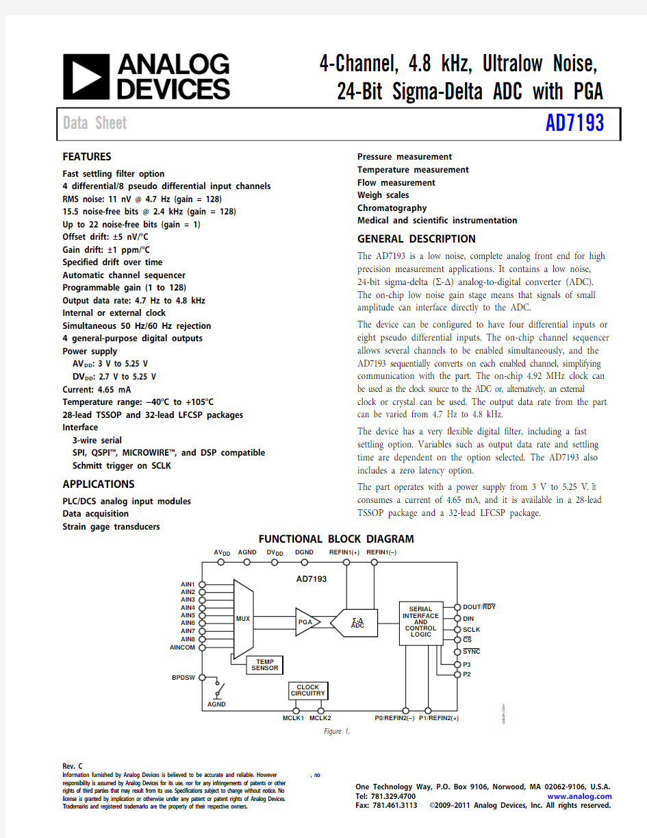
The AD7193 is a low noise, complete analog front end for high precision measurement applications. It contains a low noise, 24-bit sigma-delta (Σ-Δ) analog-to-digital converter (ADC). The on-chip low noise gain stage means that signals of small amplitude can interface directly to the ADC.
The device can be configured to have four differential inputs or eight pseudo differential inputs. The on-chip channel sequencer allows several channels to be enabled simultaneously, and the AD7193 sequentially converts on each enabled channel, simplifying communication with the part. The on-chip 4.92 MHz clock can be used as the clock source to the ADC or, alternatively, an external clock or crystal can be used. The output data rate from the part can be varied from 4.7 Hz to 4.8 kHz.
The device has a very flexible digital filter, including a fast settling option. Variables such as output data rate and settling time are dependent on the option selected. The AD7193 also includes a zero latency option.
The part operates with a power supply from 3 V to 5.25 V . It consumes a current of 4.65 mA, and it is available in a 28-lead TSSOP package and a 32-lead LFCSP package.
FUNCTIONAL BLOCK DIAGRAM
DV DGND
REFIN1(+)
REFIN1(–)
AIN1AIN2AIN3AIN4AINCOM
BPDSW
DOUT/RDY DIN CS SYNC
P3P2
AV AGND
AIN5AIN6AIN7AIN808367-001
Figure 1.
AD7193
Data Sheet
Rev. C | Page 2 of 56
TABLE OF CONTENTS
Features .............................................................................................. 1 Applications ....................................................................................... 1 General Description ......................................................................... 1 Functional Block Diagram .............................................................. 1 Revision History ............................................................................... 3 Specifications ..................................................................................... 4 Timing Characteristics ................................................................ 8 Absolute Maximum Ratings .......................................................... 10 Thermal Resistance .................................................................... 10 ESD Caution ................................................................................ 10 Pin Configurations and Function Descriptions ......................... 11 Typical Performance Characteristics ........................................... 15 RMS Noise and Resolution............................................................ 18 Sinc 4 Chop Disabled ................................................................... 18 Sinc 3 Chop Disabled ................................................................... 19 Fast Settling ................................................................................. 20 On-Chip Registers .......................................................................... 21 Communications Register ......................................................... 22 Status Register ............................................................................. 23 Mode Register ............................................................................. 24 Configuration Register .............................................................. 27 Data Register ............................................................................... 29 ID Register ................................................................................... 29 GPOCON Register ..................................................................... 29 Offset Register ............................................................................. 30 Full-Scale Register ...................................................................... 30 ADC Circuit Information .............................................................. 31 Overview ...................................................................................... 31 Analog Input Channel ............................................................... 32 Programmable Gain Array (PGA) . (32)
Reference ..................................................................................... 32 Reference Detect ......................................................................... 33 Bipolar/Unipolar Configuration .............................................. 33 Data Output Coding .................................................................. 33 Burnout Currents ....................................................................... 33 Channel Sequencer .................................................................... 33 Digital Interface .......................................................................... 34 Reset ............................................................................................. 38 System Synchronization ............................................................ 38 Enable Parity ............................................................................... 38 Clock ............................................................................................ 38 Bridge Power-Down Switch ...................................................... 38 Temperature Sensor ................................................................... 39 Logic Outputs ............................................................................. 39 Calibration................................................................................... 39 Digital Filter .................................................................................... 41 Sinc 4 Filter (Chop Disabled) ..................................................... 41 Sinc 3 Filter (Chop Disabled) ..................................................... 43 Chop Enabled (Sinc 4 Filter) ...................................................... 45 Chop Enabled (Sinc 3 Filter) ...................................................... 47 Fast Settling Mode (Sinc 4 Filter) ............................................... 48 Fast Settling Mode (Sinc 3 Filter) ............................................... 50 Fast Settling Mode (Chop Enabled) ......................................... 51 Summary of Filter Options ....................................................... 52 Grounding and Layout .................................................................. 53 Applications Information .............................................................. 54 Flowmeter .................................................................................... 54 Outline Dimensions ....................................................................... 55 Ordering Guide .. (55)
Data Sheet
AD7193
Rev. C | Page 3 of 56
REVISION HISTORY
12/11—Rev. B to Rev. C
Moved Revision History Section ..................................................... 3 Changes to Table 6 .......................................................................... 13 4/10—Rev. A to Rev. B
Added 32-Lead LFCSP ...................................................... Universal Changes to Table 7 .......................................................................... 17 Changes to Communications Register, Table 16 ......................... 20 Updated Outline Dimensions ........................................................ 54 Changes to Ordering Guide ........................................................... 54 9/09—Rev. 0 to Rev. A
Changes to Internal/External Clock, Internal Clock Frequency Parameter, Table 1 ............................................................................. 5 Changes to Figure 7 and Figure 8 .. (14)
Changes to Table 6 .......................................................................... 17 Changes to Table 9 .......................................................................... 18 Changes to Table 12, Table 13, and Table 14 ............................... 19 Changes to Table 19 ........................................................................ 24 Changes to Table 22 and Table 23 ................................................. 27 Changes to Offset Register and Full-Scale Register Sections .... 29 Changes to Reference Section ....................................................... 31 Changes to Data Output Coding Section .................................... 32 Changes to Sinc 4 50 Hz/60 Hz Rejection Section ....................... 41 Changes to Sinc 3 50 Hz/60 Hz Rejection Section ....................... 43 Changes to 50 Hz/60 Hz Rejection, Sinc 4 Filter Section ............ 47 Changes to Summary of Filter Options Section and Table 35 .. 52 7/09—Revision 0: Initial Version
AD7193
Data Sheet
Rev. C | Page 4 of 56
SPECIFICATIONS
AV DD = 3 V to 5.25 V , DV DD = 2.7 V to 5.25 V , AGND = DGND = 0 V; REFINx(+) = 2.5 V or AV DD , REFINx(?) = AGND, MCLK = 4.92 MHz, T A = T MIN to T MAX , unless otherwise noted. Table 1.
Parameter Min Typ Max Unit Test Conditions/Comments 1 ADC
Output Data Rate 4.7 4800 Hz Chop disabled
1.17 1200 Hz Chop enabled, sinc 4 filter
1.56 1600 Hz Chop enabled, sinc 3 filter No Missing Codes 2 24 Bits FS[9:0]3 > 1, sinc 4 filter
24 Bits FS[9:0]3 > 4, sinc 3 filter
Resolution
See the RMS Noise and Resolution section RMS Noise and Output Data Rates
See the RMS Noise and Resolution section Integral Nonlinearity
Gain = 12 ±2 ±10 ppm of FSR AV DD = 5 V
±2 ±15 ppm of FSR AV DD = 3 V Gain > 1 ±5 ±30 ppm of FSR AV DD = 5 V
±15
±30 ppm of FSR AV DD = 3 V Offset Error 4, 5 ±150/gain μV Chop disabled
±1 μV Chop enabled, AV DD = 5 V
±0.5
μV Chop enabled, AV DD = 3 V Offset Error Drift vs. Temperature ±150/gain nV/°C Gain = 1 to 16; chop disabled ±5 nV/°C Gain = 32 to 128; chop disabled
±5 nV/°C Chop enabled Offset Error Drift vs. Time 25 nV/1000 hours Gain > 32
Gain Error 4 ±0.001 % AV DD = 5 V, gain = 1, T A = 25°C (factory calibration conditions)
?0.39 % Gain = 128, before full-scale calibration (see Table 27)
±0.003 % Gain > 1, after internal full-scale calibration, AV DD ≥ 4.75 V
±0.005 % Gain > 1, after internal full-scale calibration, AV DD < 4.75 V Gain Drift vs. Temperature ±1 ppm/°C Gain Drift vs. Time 10 ppm/
1000 hours Gain = 1
Power Supply Rejection 90 dB Gain = 1, V IN = 1 V
95 110 dB Gain > 1, V IN = 1 V/gain Common-Mode Rejection
@ DC 110 dB Gain = 1, V IN = 1 V
@ DC
105 dB Gain > 1, V IN = 1 V/gain
@ 50 Hz, 60 Hz 2 120 dB 10 Hz output data rate, 50 Hz ± 1 Hz, 60 Hz ± 1 Hz
@ 50 Hz 2 120 dB 50 Hz output data rate, 50 Hz ± 1 Hz @ 60 Hz 2 120 dB 60 Hz output data rate, 60 Hz ± 1 Hz @ 50 Hz 2 115 dB Fast settling, FS[9:0]3 = 6, average by 16, 50 Hz ± 1 Hz
@ 60 Hz 2
115
dB
Fast settling, FS[9:0]3 = 5, average by 16, 60 Hz ± 1 Hz
Data Sheet
AD7193
Rev. C | Page 5 of 56
Parameter
Min Typ Max Unit Test Conditions/Comments 1 Normal-Mode Rejection 2 Sinc 4 Filter
Internal Clock
@ 50 Hz, 60 Hz
100 dB 10 Hz output data rate, 50 Hz ± 1 Hz, 60 Hz ± 1 Hz
74 dB 50 Hz output data rate, REJ606 = 1, 50 Hz ± 1 Hz, 60 Hz ± 1 Hz
@ 50 Hz 96 dB 50 Hz output data rate, 50 Hz ± 1 Hz @ 60 Hz 97 dB 60 Hz output data rate, 60 Hz ± 1 Hz External Clock
@ 50 Hz, 60 Hz 120 dB 10 Hz output data rate, 50 Hz ± 1 Hz, 60 Hz ± 1 Hz
82 dB 50 Hz output data rate, REJ606 = 1, 50 Hz ± 1 Hz, 60 Hz ± 1 Hz
@ 50 Hz 120 dB 50 Hz output data rate, 50 Hz ± 1 Hz @ 60 Hz 120 dB 60 Hz output data rate, 60 Hz ± 1 Hz Sinc 3
Filter
Internal Clock
@ 50 Hz, 60 Hz
75 dB 10 Hz output data rate, 50 Hz ± 1 Hz, 60 Hz ± 1 Hz
60 dB 50 Hz output data rate, REJ606 = 1, 50 Hz ± 1 Hz, 60 Hz ± 1 Hz
@ 50 Hz 70 dB 50 Hz output data rate, 50 Hz ± 1 Hz @ 60 Hz 70 dB 60 Hz output data rate, 60 Hz ± 1 Hz External Clock
@ 50 Hz, 60 Hz 100 dB 10 Hz output data rate, 50 Hz ± 1 Hz, 60 Hz ± 1 Hz
@ 50 Hz
67
dB 50 Hz output data rate, REJ606 = 1, 50 Hz ± 1 Hz, 60 Hz ± 1 Hz
@ 50 Hz 95 dB 50 Hz output data rate, 50 Hz ± 1 Hz @ 60 Hz 95 dB 60 Hz output data rate, 60 Hz ± 1 Hz Fast Settling Internal Clock
@ 50 Hz 26 dB FS[9:0]3 = 6, average by 16, 50 Hz ± 0.5 Hz @ 60 Hz 26 dB FS[9:0]3 = 5, average by 16, 60 Hz ± 0.5 Hz External Clock
@ 50 Hz 40 dB FS[9:0]3 = 6, average by 16, 50 Hz ± 0.5 Hz @ 60 Hz
40 dB FS[9:0]3 = 5, average by 16, 60 Hz ± 0.5 Hz ANALOG INPUTS
Differential Input Voltage Ranges
±V REF /gain
V V REF = REFINx(+) ? REFINx(?), gain = 1 to 128
?(AV DD ? 1.25 V)/gain +(AV DD ? 1.25 V)/gain V Gain > 1 Absolute AIN Voltage Limits 2
Unbuffered Mode AGND ? 0.05 AV DD + 0.05 V Buffered Mode AGND + 0.25 AV DD ? 0.25 V Analog Input Current Buffered Mode
Input Current 2 ?2 +2 nA Gain = 1
?3 +3 nA Gain > 1 Input Current Drift ±5 pA/°C Unbuffered Mode
Input Current
±3.5 μA/V Gain = 1, input current varies with input voltage
±1 μA/V Gain > 1
Input Current Drift
±0.05 nA/V/°C External clock
±1.6
nA/V/°C
Internal clock
AD7193 Data Sheet
Rev. C | Page 6 of 56
Data Sheet
AD7193
Rev. C | Page 7 of 56
Parameter
Min Typ Max Unit Test Conditions/Comments 1 SYSTEM CALIBRATION 2
Full-Scale Calibration Limit
1.05 × FS V Zero-Scale Calibration Limit ?1.05 × FS V
Input Span
0.8 × FS 2.1 × FS V POWER REQUIREMENTS 7 Power Supply Voltage AV DD ? AGND 3 5.25 V DV DD ? DGND
2.7 5.25 V Power Supply Currents
AI DD Current 0.85 1 mA Gain = 1, buffer off 1 1.25 mA Gain = 1, buffer on 2.8 3.6 mA Gain = 8, buffer off 3.2 3.9 mA Gain = 8, buffer on
3.8
4.7 mA Gain = 16 to 128, buffer off
4.3
5.3 mA Gain = 16 to 128, buffer on DI DD Current 0.35 0.4 mA DV DD = 3 V 0.5 0.6 mA DV DD = 5 V
1.5 mA External crystal used I DD
3
μA
Power-down mode
1 Temperature range: ?40°C to +105°C.
2
Specification is not production tested but is supported by characterization data at initial product release. 3
FS[9:0] is the decimal equivalent of Bit FS9 to Bit FS0 in the mode register. 4
Following a system or internal zero-scale calibration, the offset error is in the order of the noise for the programmed gain and output data rate selected. A system full-scale calibration reduces the gain error to the order of the noise for the programmed gain and output data rate. 5
The analog inputs are configured for differential mode. 6
REJ60 is a bit in the mode register. When the first notch of the sinc filter is at 50 Hz, a notch is placed at 60 Hz when REJ60 is set to 1. This gives simultaneous 50 Hz/60 Hz rejection. 7
Digital inputs equal to DV DD or DGND.
AD7193
Data Sheet
Rev. C | Page 8 of 56
TIMING CHARACTERISTICS
AV DD = 3 V to 5.25 V , DV DD = 2.7 V to 5.25 V , AGND = DGND = 0 V , Input Logic 0 = 0 V , Input Logic 1 = DV DD , unless otherwise noted.
1 Sample tested during initial release to ensure compliance. All input signals are specified with t R = t F = 5 ns (10% to 90% of DV DD ) and timed from a voltage level of 1.6 V. 2
See Figure 3 and Figure 4. 3
These numbers are measured with the load circuit shown in Figure 2 and defined as the time required for the output to cross the V OL or V OH limits. 4
The SCLK active edge is the falling edge of SCLK. 5
These numbers are derived from the measured time taken by the data output to change 0.5 V when loaded with the circuit shown in Figure 2. The measured number is then extrapolated back to remove the effects of charging or discharging the 50 pF capacitor. This means that the times quoted in the timing characteristics are the true bus relinquish times of the part and, as such, are independent of external bus loading capacitances. 6 RDY returns high after a read of the data register. In single conversion mode and continuous conversion mode, the same data can be read again, if required, while RDY is high, although care should be taken to ensure that subsequent reads do not occur close to the next output update. If the continuous read feature is enabled, the digital word can be read only once.
Circuit and Timing Diagrams
DD = 5V,DD = 3V)
DD = 5V,DD = 3V)
1.6V
TO OUTPUT
PIN
08367-002
Figure 2. Load Circuit for Timing Characterization
Data Sheet
AD7193
Rev. C | Page 9 of 56
CS (I)
DOUT/RDY (O)
I = INPUT, O = OUTPUT
08367-003
Figure 3. Read Cycle Timing Diagram
I = INPUT, O = OUTPUT
CS (I)
SCLK (I)
DIN (I)
08367-004
Figure 4. Write Cycle Timing Diagram
AD7193
Data Sheet
Rev. C | Page 10 of 56
ABSOLUTE MAXIMUM RATINGS
T A = 25°C, unless otherwise noted. Table 3.
Parameter Rating
AV DD to AGND ?0.3 V to +6.5 V DV DD to AGND ?0.3 V to +6.5 V AGND to DGND
?0.3 V to +0.3 V
Analog Input Voltage to AGND ?0.3 V to AV DD + 0.3 V Reference Input Voltage to AGND ?0.3 V to AV DD + 0.3 V Digital Input Voltage to DGND ?0.3 V to DV DD + 0.3 V Digital Output Voltage to DGND ?0.3 V to DV DD + 0.3 V AINx/Digital Input Current 10 mA
Operating Temperature Range ?40°C to +105°C Storage Temperature Range ?65°C to +150°C Maximum Junction Temperature 150°C Lead Temperature, Soldering Reflow
260°C
Stresses above those listed under Absolute Maximum Ratings may cause permanent damage to the device. This is a stress rating only; functional operation of the device at these or any other conditions above those indicated in the operational
section of this specification is not implied. Exposure to absolute maximum rating conditions for extended periods may affect device reliability. THERMAL RESISTANCE
θJA is specified for the worst-case conditions, that is, a device soldered in a circuit board for the surface-mount packages. Table 4. Thermal Resistance
Package Type θJA θJC Unit 28-Lead TSSOP 97.9 14 °C/W 32-Lead LFCSP
32.5
32.71
°C/W
ESD CAUTION
Data Sheet
AD7193
Rev. C | Page 11 of 56
PIN CONFIGURATIONS AND FUNCTION DESCRIPTIONS
NC = NO CONNECT
MCLK2SCLK CS P1/REFIN2(+)P2P3
MCLK1DOUT/RDY SYNC DV DD AGND DGND AV DD P0/REFIN2(–)
NC
AINCOM AIN4AIN2AIN1BPDSW REFIN1(–)REFIN1(+)AIN5
AIN3AIN6
AIN7AIN8DIN 08367-005
Figure 5. 28-lead TSSOP Pin Configuration
AD7193 Data Sheet
Rev. C | Page 12 of 56
Data Sheet
AD7193
Rev. C | Page 13 of 56
08367-065
NOTES
1. NC = NO CONNECT.
2. CONNECT EXPOSED PAD TO AGND.
24DV DD 23AV DD 22DGND 21AGND 20BPDSW 19NC
18REFIN1(–)17
REFIN1(+)
12345678
P3P2
P1/REFIN2(+)P0/REFIN2(–)
NC NC NC AINCOM
910111213141516
A I N 1A I N 2A I N 3A I N 4A I N 5A I N 6A I N 7A I N 83231302928272625
C S S C L K M C L K 2M C L K 1
D I N D O U T /R D Y N C S Y N C
TOP VIEW (Not to Scale)
AD7193
Figure 6. 32-Lead LFCSP Pin Configuration
Table 6. 32-Lead LFCSP Pin Function Descriptions
Pin No. Mnemonic Description
1 P3 Digital Output Pin. This pin can function as a general-purpose output bit referenced between AV DD and AGND.
2 P2
Digital Output Pin. This pin can function as a general-purpose output bit referenced between AV DD and AGND.
3
P1/REFIN2(+)
Digital Output Pin/Positive Reference Input. This pin functions as a general-purpose output bit referenced between AV DD and AGND. When the REFSEL bit in the configuration register = 1, this pin functions as REFIN2(+). An external reference can be applied between REFIN2(+) and REFIN2(?). REFIN2(+) can lie
anywhere between AV DD and AGND + 1 V. The nominal reference voltage, (REFIN2(+) ? REFIN2(?)), is AV DD , but the part functions with a reference from 1 V to AV DD .
4 P0/REFIN2(?) Digital Output Pin/Negative Reference Input. This pin functions as a general-purpose output bit referenced between AV DD and AGND. When the REFSEL bit in the configuration register = 1, this pin functions as REFIN2(?). This reference input can lie anywhere between AGND and AV DD ? 1 V. 5, 6, 7, 19, 26 NC No Connect. Tie these pins to AGND.
8 AINCOM Analog Input AIN1 to Analog Input AIN8 are referenced to this input when configured for pseudo differential operation.
9 AIN1 Analog Input. This pin can be configured as the positive input of a fully differential input pair when used with AIN2 or as a pseudo differential input when used with AINCOM.
10 AIN2 Analog Input. This pin can be configured as the negative input of a fully differential input pair when used with AIN1 or as a pseudo differential input when used with AINCOM.
11 AIN3 Analog Input. This pin can be configured as the positive input of a fully differential input pair when used with AIN4 or as a pseudo differential input when used with AINCOM.
12 AIN4 Analog Input. This pin can be configured as the negative input of a fully differential input pair when used with AIN3 or as a pseudo differential input when used with AINCOM.
13 AIN5 Analog Input. This pin can be configured as the positive input of a fully differential input pair when used with AIN6 or as a pseudo differential input when used with AINCOM.
14 AIN6 Analog Input. This pin can be configured as the negative input of a fully differential input pair when used with AIN5 or as a pseudo differential input when used with AINCOM.
15 AIN7 Analog Input. This pin can be configured as the positive input of a fully differential input pair when used with AIN8 or as a pseudo differential input when used with AINCOM.
16 AIN8 Analog Input. This pin can be configured as the negative input of a fully differential input pair when used with AIN7 or as a pseudo differential input when used with AINCOM.
17 REFIN1(+) Positive Reference Input. An external reference can be applied between REFIN1(+) and REFIN1(?). REFIN1(+) can lie anywhere between AV DD and AGND + 1 V. The nominal reference voltage, (REFIN1(+) ? REFIN1(?)), is AV DD , but the part functions with a reference from 1 V to AV DD .
18 REFIN1(?) Negative Reference Input. This reference input can lie anywhere between AGND and AV DD ? 1 V. 20
BPDSW
Bridge Power-Down Switch to AGND.
AD7193 Data Sheet
Rev. C | Page 14 of 56
Data Sheet
AD7193
Rev. C | Page 15 of 56
TYPICAL PERFORMANCE CHARACTERISTICS
08367-006
200
400
600
800
1000
SAMPLE
C O
D E
8,387,468
8,387,4708,387,4728,387,4748,387,4768,387,4788,387,480
8,387,4828,387,4848,387,486
Figure 7. Noise (V REF = AV DD = 5 V, Output Data Rate = 4.7 Hz,
Gain = 128, Chop Disabled, Sinc 4 Filter)
08367-007
50100150200
8,387,4728,387,4768,387,4808,387,484
CODE
O C C U R R E N C E
Figure 8. Noise Distribution Histogram (V REF = AV DD = 5 V,
Output Data Rate = 4.7 Hz, Gain = 128, Chop Disabled, Sinc 4 Filter)
08367-00
8
8,388,830
8,388,840
8,388,8508,388,8608,388,8708,388,8808,388,890
8,388,9008,388,9108,388,92002004006008001000SAMPLE
C O
D E
Figure 9. Noise (V REF = AV DD = 5 V, Output Data Rate = 2400 Hz,
Gain = 1, Chop Disabled, Sinc 4 Filter) 08367-00
9
10
20
30
40
50
8,388,830
8,388,860
8,388,8908,388,920
CODE
O C C U R R E N C E
Figure 10. Noise Distribution Histogram (V REF = AV DD = 5 V, Output Data Rate = 2400 Hz, Gain = 1, Chop Disabled, Sinc 4 Filter)
08367-010
8,388,864
8,388,866
8,388,8688,388,870
8,388,8728,388,874
8,388,8768,388,878
8,388,8800200400
6008001000
SAMPLE
C O
D E
Figure 11. Noise (V REF = AV DD = 5 V, Output Data Rate = 42.1 Hz (FS[9:0] = 6,
Average by 16), Gain = 1, Chop Disabled, Sinc 4 Filter)
08367-011
50
100
150
200
8,388,864
8,388,8688,388,872
8,388,8768,388,880
CODE
O C C U R R E N C E
Figure 12. Noise Distribution Histogram (V REF = AV DD = 5 V, Output Data Rate = 42.1 Hz (FS[9:0] = 6, Average by 16), Gain = 1, Chop Disabled, Sinc 4 Filter)
AD7193
Data Sheet
Rev. C | Page 16 of 56
5–2–10
123
4–4
–3–2–101234
I N L (p p m o f F S R )
V IN (V)
08367-01
2
Figure 13. INL (Gain = 1)
20–20–15–10
–505
10
15–0.03
–0.02–0.0100.010.020.03I N L (p p m o f F S R )
V IN (V)
08367-01
3
Figure 14. INL (Gain = 128)
170168166
164162160156158154–60
–40–20020406080100120O F F S E T (μV )
TEMPERATURE (°C)
08367-01
4
Figure 15. Offset vs. Temperature (Gain = 1, Chop Disabled) 0.4–1.4
–1.2
–1.0
–0.8–0.6–0.4–0.2
0.2–60
–40–20020406080100120
O F F S E T (μV )
TEMPERATURE (°C)
08367-01
5
Figure 16. Offset vs. Temperature (Gain = 128, Chop Disabled)
–60
–40–20020406080100120
G A I N
TEMPERATURE (°C)
08367-01
60.999988
0.999990
0.999992
0.9999940.9999960.9999981.000000
1.000002
1.0000041.0000061.000008
Figure 17. Gain vs. Temperature (Gain = 1)
–60
–40–20020406080100120
G A I N
TEMPERATURE (°C)
08367-0
17
127.988
127.990127.992127.994127.996127.998
128.000128.002128.004
Figure 18. Gain vs. Temperature (Gain = 128)
Data Sheet
AD7193
Rev. C | Page 17 of 56
08367-018
14
16
18
20
22
24
110100
OUTPUT DATA RATE (Hz)
1k 10k N O I S E F R E E R E S O L U T I O N (B i t s
)
Figure 19. Noise Free Resolution (Sinc 4 Filter, Chop Disabled, V REF = 5 V)
08367-019
10
121416182022
24110100
1k 10k
OUTPUT DATA RATE (Hz)
N O I S E F R E E R E S O L U T I O N (B i t s
)
Figure 20. Noise Free Resolution (Sinc 3
Filter, Chop Disabled, V REF = 5 V)
08367-022
16
17
18192022
21231101001k
OUTPUT DATA RATE (Hz)
N O I S E F R E E R E S O L U T I O N (B i t s
)
Figure 21. Noise Free Resolution in Fast Settling Mode (V REF = 5 V, Averaging by 16, Sinc 4 Filter, Chop Disabled)
AD7193
Data Sheet
Rev. C | Page 18 of 56
RMS NOISE AND RESOLUTION
The following tables show the rms noise, peak-to-peak noise, effective resolution, and noise free (peak-to-peak) resolution of the AD7193 for various output data rates and gain settings with chop disabled for the sinc 4 and sinc 3 filters and for fast settling mode. The numbers given are for the bipolar input range with an external 5 V reference. These numbers are typical and are
generated with a differential input voltage of 0 V when the ADC
is continuously converting on a single channel. It is important to note that the effective resolution is calculated using the rms noise, whereas the peak-to-peak resolution is calculated based on peak-to-peak noise. The peak-to-peak resolution represents the resolution for which there is no code flicker. With chop enabled, the resolution improves by 0.5 bits.
SINC 4 CHOP DISABLED
Table 7. RMS Noise (nV) vs. Gain and Output Data Rate
Filter Word (Decimal) Output Data Rate (Hz) Settling Time (ms) Gain of
1 8 16 3
2 64 128 102
3 4.7 852.5 340 53 3
4 18 12 11 640 7.
5 533 410 67 40 24 14 13 480 10 400 460 7
6 45 28 16 15 96 50 80 950 150 80 50 3
7 31 80 60 66.7 1000 160 90 54 40 35 32 150 26.7 1600 250 140 83 63 55 16 300 13.3 2300 340 190 120 90 79 5 960 4.17 4200 610 350 210 160 140 2 2400 1.67 7100 1000 570 350 260 230 1
4800
0.83
26,000
3400
1700
910
530
380
Table 8. Peak-to-Peak Noise (nV) vs. Gain and Output Data Rate
Filter Word (Decimal) Output Data Rate (Hz) Settling Time (ms) Gain of
1 8 16 3
2 64
128 1023 4.7 852.5 2200 340 190 110 70 65 640 7.5 533 2700 410 230 130 90 85 480 10 400 3000 450 260 150 100 95 96 50 80 6000 890 500 320 230 200 80 60 66.7 6600 1000 560 350 250 220 32 150 26.7 10,000 1500 920 540 400 370 16 300 13.3 14,000 2200 1300 800 600 530 5 960 4.17 28,000 4100 2400 1400 1000 900 2 2400 1.67 49,000 7000 3800 2400 1800 1700 1
4800
0.83
175,000
23,000
12,000 6100
3500
2600
Table 9. Effective Resolution (Peak-to-Peak Resolution) vs. Gain and Output Data Rate
Filter Word (Decimal) Output Data Rate (Hz) Settling Time (ms) Gain of 1
1
8
16 32 64
128
1023 4.7 852.5 24 (22.1) 24 (21.8) 24 (21.6) 24 (21.4) 23.6 (21.1) 22.8 (20.2) 640 7.5 533 24 (21.8) 24 (21.5) 23.9 (21.4) 23.6 (21.2) 23.4 (20.7) 22.5 (19.8) 480 10 400 24 (21.7) 24 (21.4) 23.7 (21.2) 23.4 (21) 23.2 (20.6) 22.3 (19.6) 96 50 80 23.3 (20.7) 23 (20.4) 22.9 (20.3) 22.6 (19.9) 22 (19.4) 21.3 (18.6) 80 60 66.7 23.3 (20.5) 22.9 (20.3) 22.8 (20.1) 22.5 (19.8) 21.9 (19.3) 21.1 (18.4) 32 150 26.7 22.6 (19.9) 22.3 (19.7) 22.1 (19.4) 21.8 (19.1) 21.2 (18.6) 20.4 (17.7) 16 300 13.3 22.1 (19.4) 21.8 (19.1) 21.6 (18.9) 21.3 (18.6) 20.7 (18) 19.9 (17.2) 5 960 4.17 21.2 (18.4) 21 (18.2) 20.8 (18) 20.5 (17.8) 19.9 (17.3) 19.1 (16.4) 2 2400 1.67 20.4 (17.6) 20.3 (17.4) 20.1 (17.3) 19.8 (17) 19.2 (16.4) 18.4 (15.5) 1
4800 0.83
18.6 (15.8) 18.5 (15.7)
18.5 (15.7) 18.4 (15.6)
18.2 (15.4) 17.6 (14.9)
1
The output peak-to-peak (p-p) resolution is listed in parentheses.
Data Sheet
AD7193
Rev. C | Page 19 of 56
SINC 3 CHOP DISABLED
Table 10. RMS Noise (nV) vs. Gain and Output Data Rate
Filter Word (Decimal) Output Data Rate (Hz) Settling Time (ms) Gain of 1 8 16 32 64 128 1023 4.7 639.4 340 58 35 20 13 11 640 7.5 400 410 72 41 25 16 14 480 10 300 490 90 45 28 18 16 96 50 60 1000 160 85 54 38 34 80 60 50 1100 170 95 59 41 37 32 150 20 1700 260 150 88 66 59 16 300 10 2400 350 200 130 94 85 5 960 3.13 6400 870 470 270 190 160 2 2400 1.25 115,000 14,000 7000 3600 1800 950 1
4800
0.625
860,000
110,000
54,000
27,000
14,000
7000
Table 11. Peak-to-Peak Noise (nV) vs. Gain and Output Data Rate
Filter Word (Decimal) Output Data Rate (Hz) Settling Time (ms) Gain of 1 8 16 32 64 128 1023 4.7 639.4 2200 350 220 130 80 65 640 7.5 400 2700 450 270 160 100 88 480 10 300 3000 520 310 180 120 100 96 50 60 6400 990 540 370 250 230 80 60 50 7000 1100 610 390 270 250 32 150 20 11,000 1700 980 580 440 390 16 300 10 16,000 2300 1400 860 630 560 5 960 3.13 40,000 5700 3100 1800 1300 1100 2 2400 1.25 730,000 93,000 47,000 24,000 12,000 6100 1
4800
0.625
5,700,000
730,000
360,000
180,000
93,000
45,000
Table 12. Effective Resolution (Peak-to-Peak Resolution) vs. Gain and Output Data Rate
Filter Word (Decimal) Output Data Rate (Hz) Settling Time (ms) Gain of 1
1
8
16
32
64
128
1023 4.7 639.4 24 (22.1) 24 (21.8) 24 (21.4) 23.9 (21.2) 23.5 (20.9) 22.8 (20.2) 640 7.5 400 24 (21.8) 24 (21.4) 23.9 (21.1) 23.6 (20.9) 23.2 (20.6) 22.4 (19.8) 480 10 300 24 (21.7) 23.8 (21.2) 23.7 (20.9) 23.4 (20.7) 23 (20.3) 22.2 (19.6) 96 50 60 23.3 (20.6) 22.9 (20.3) 22.9 (20.1) 22.5 (19.7) 22 (19.3) 21.1 (18.4) 80 60 50 23.1 (20.4) 22.8 (20.1) 22.7 (20) 22.3 (19.6) 21.9 (19.1) 21 (18.3) 32 150 20 22.5 (19.8) 22.2 (19.5) 22 (19.3) 21.8 (19) 21.2 (18.4) 20.3 (17.6) 16 300 10 22 (19.3) 21.8 (19.1) 21.6 (18.8) 21.2 (18.5) 20.7 (17.9) 19.8 (17.1) 5 960 3.13 20.6 (17.9) 20.5 (17.7) 20.3 (17.6) 20.1 (17.4) 19.6 (16.9) 18.9 (16.1) 2 2400 1.25 16.5 (13.7) 16.4 (13.7) 16.4 (13.7) 16.4 (13.7) 16.4 (13.7) 16.4 (13.6) 1
4800 0.625
13.5 (10.8)
13.5 (10.7)
13.5 (10.7)
13.5 (10.7)
13.5 (10.7)
13.5 (10.7)
1
The output peak-to-peak (p-p) resolution is listed in parentheses.
AD7193
Data Sheet
Rev. C | Page 20 of 56
FAST SETTLING
Table 13. RMS Noise (nV) vs. Gain and Output Data Rate
Filter Word (Decimal) Average Output Data
Rate (Hz) Settling
Time (ms) Gain of
1 8 16 3
2 64 128 96 16 2.6
3 380 380 87 52 33 15 11 30 16 8.
4 118.7
5 620 140 71 43 30 21
6 16 42.10 23.75 1300 270 150 82 56 4
7 5 16 50.53 19.79 1500 280 160 8
8 61 50 2 16 126.32 7.92 2300 380 210 130 88 77 1
16 252.63
3.96
3400
520
290
180
130
110
Table 14. Peak-to-Peak Noise (nV) vs. Gain and Output Data Rate
Filter Word (Decimal) Average Output Data Rate (Hz) Settling Time (ms) Gain of
1 8 16 3
2 64 128 96 16 2.6
3 380 2500 450 260 180 100 70 30 16 8.
4 118.7
5 4000 900 470 280 190 130
6 16 42.10 23.75 8500 1800 950 540 360 300 5 16 50.53 19.79 9500 1900 1000 580 390 330 2 16 126.32 7.92 14,000 2800 1500 850 580 510 1
16
252.63
3.96
22,000
3800
2000
1200
820
740
Table 15. Effective Resolution (Peak-to-Peak Resolution) vs. Gain and Output Data Rate
Filter Word (Decimal) Average Output Data
Rate (Hz) Settling
Time (ms) Gain of 1
1
8
16 32 64
128
96 16 2.63 380 24 (21.9) 23.8 (21.4) 23.5 (21.2) 23.2 (20.7) 23.2 (20.6) 22.8 (20.1) 30 16 8.4 118.75 23.9 (21.3) 23.6 (20.4) 23.1 (20.3) 22.8 (20.1) 22.3 (19.6) 21.8 (19.2) 6 16 42.10 23.75 22.9 (20.2) 22.1 (19.4) 22 (19.3) 21.9 (19.1) 21.4 (18.7) 20.7 (18) 5 16 50.53 19.79 22.7 (20) 22.1 (19.3) 21.9 (19.3) 21.8 (19) 21.3 (18.6) 20.6 (17.9) 2 16 126.32 7.92 22.1 (19.4) 21.6 (18.8) 21.5 (18.7) 21.2 (18.5) 20.8 (18) 20 (17.2) 1
16 252.63 3.96
21.5 (18.8) 21.2 (18.3)
21 (18.3) 20.7 (18)
20.2 (17.5) 19.4 (16.7)
1
The output peak-to-peak (p-p) resolution is listed in parentheses.