R7779A

Burst Triple Mode PWM Controller with Integrated HV Start-up Device for Zero Power Monitor Application
Features
Integrated HV Start-up Device
Enable/Disable Function UVLO: 9V/16.5V
Current Mode Control
Built-in 65kHz Operation Frequency Built-in Jittering Frequency
Internal PWM Leading Edge Blanking Internal Slope Compensation
Compensated Burst Triple Mode PWM Cycle-by-Cycle Current Limit Internal Auto Recovery OVP Internal Auto Recovery OLP Internal Auto Recovery OTP CS Pin Open Protection
Secondary Rectifier Short Protection Soft Driving for Reducing EMI Noise High Noise Immunity
RoHS Compliant and Halogen Free
Applications
Switching AC/DC Adaptor TV and Monitor Application
Low Standby Power Home Appliance
General Description
The R7779A is a high-performance current mode PWM controller with integrated HV start-up device inside. During start-up, a current source through integrated HV device to charge VDD capacitor for quick start-up while it dissipates no loss in normal operation.
The R7779A provides the users a superior AC/DC power application of higher efficiency, few external component counts, and low cost solution. It features frequency jitter,Under Voltage LockOut (UVLO), Leading Edge Blanking (LEB), internal slope compensation in the tiny SOP-7package. It offers complete protection coverage with Over T emperature Protection (OTP), Over Load Protection (OLP)and Over Voltage Protection (OVP).
Moreover, it also provides a special interface for zero power application when the converter is in sleeping mode. EN/DIS pin receives ON/OFF signal from secondary scalar controller. During turning off, the controller will be shutdown completely with pretty low power consumption.
Ordering Information
Note :
Richpower Green products are :
RoHS compliant and compatible with the current
requirements of IPC/JEDEC J-STD-020.
Suitable for use in SnPb or Pb-free soldering processes.
Marking Information
For marking information, contact our sales representative directly or through a Richpower distributor located in your area, otherwise visit our website for detail.
G : Green (Halogen Free with Commer-cial Standard)
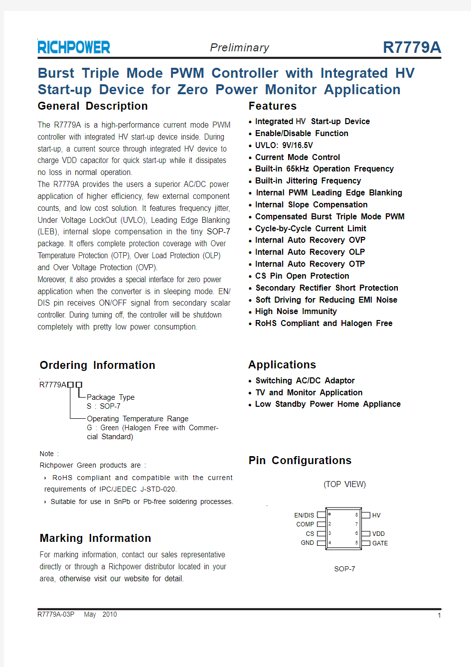
Pin Configurations
(TOP VIEW)
SOP-7
EN/DIS COMP
CS GND
HV GATE
VDD
Pin Description
O +
O -Typical Application Circuit
Block Diagram
VDD
Electrical Characteristics
To be continued
Recommended Operating Conditions (Note 4)
Supply Input Voltage, V DD -----------------------------------------------------------------------------------------12V to 25V
Ambient T emperature Range --------------------------------------------------------------------------------------?40°C to 85°C
Absolute Maximum Ratings (Note 1)
HV Pin -----------------------------------------------------------------------------------------------------------------?0.3V to 700V Supply Input Voltage, V DD -----------------------------------------------------------------------------------------?0.3V to 30V GATE Pin --------------------------------------------------------------------------------------------------------------?0.3V to 20V EN/DIS, COMP , CS Pin --------------------------------------------------------------------------------------------?0.3V to 6.5V
Power Dissipation, P D @ T A = 85°C
SOP-7------------------------------------------------------------------------------------------------------------------0.625W
Package Thermal Resistance (Note 2)
SOP-7, θJA ------------------------------------------------------------------------------------------------------------160°C/W Junction T emperature -----------------------------------------------------------------------------------------------150°C Lead Temperature (Soldering, 10 sec.)-------------------------------------------------------------------------260°C
Storage T emperature Range ---------------------------------------------------------------------------------------?65°C to 150°C
ESD Susceptibility (Note 3)
Human Body Mode (Except HV pin)----------------------------------------------------------------------------6kV Machine Mode --------------------------------------------------------------------------------------------------------200V
(V DD = 15V, T A = 25°C, unless otherwise specified)
Note 1. Stresses beyond those listed under “Absolute Maximum Ratings” may cause permanent damage to the device.
These are stress ratings only, and functional operation of the device at these or any other conditions beyond those indicated in the operational sections of the specifications is not implied. Exposure to absolute maximum rating conditions for extended periods may affect device reliability.
Note 2. θJA is measured in the natural convection at T A = 25°C on a low effective single layer thermal conductivity test board of JEDEC 51-3 thermal measurement standard.
Note 3. Devices are ESD sensitive. Handling precaution is recommended.
Note 4. The device is not guaranteed to function outside its operating conditions.
Note 5. Guaranteed by design.
Note 6. Leading edge blanking time and internal propagation delay time are guaranteed by design.
Typical Operating Characteristics
Start-up Current (I DD_ST ) vs. Temperature
010
20
30
40
50
-40
40
80
120
Temperature I D D _S T (μA )
(°C)HV Start-up Current (I JFET_ST ) vs. Temperature
0.0
1.0
2.0
3.0
4.0
-40
40
80
120
Temperature I J F E T _S T (m A )
(°
C)
On Threshold Voltage (V TH_ON ) vs. Temperature
16.0
16.416.817.217.618.0
-40
40
80
120
Temperature V T H _O N (V )
(°
C)
Off Threshold Voltage (V TH_OFF ) vs. Temperature
8.0
8.4
8.8
9.2
9.6
10.0
-40
40
80
120
Temperature V T H _O F F (V )
(°C)
Normal PWM Frequency (f OSC ) vs. Temperature
58606264
6668
-40
40
80
120
Temperature f O S C (k H z )
(°C)
Normal PWM Frequency (f OSC ) vs. V DD
5860
62
64
66
68
10
15
20
25
V DD (V)
f O S C (k H z )
Short Circuit COMP Current (I ZERO ) vs. Temperature
0.0
0.4
0.8
1.2
1.6
2.0
-40
40
80
120
Temperature I Z E R O (m A )
(°
C)
Gate Output Clamping Voltage (V CLAMP ) vs. Temperature
101214161820
-40
40
80
120
Temperature V C L A M P (V )
(°C)
Gate Output Clamping Voltage (V CLAMP ) vs. V DD
04
8
12
16
20
10
15
20
25
V DD (V)
V C L A M P (V )
Operating Current (I DD_OP ) vs. Temperature
-40
40
80
120
Temperature I D D _O P (μA )
(°C)
Operating Current (I DD_OP ) vs. V DD
10
15
20
25
V DD (V)
I D D _O P (μA )
Open-Loop Voltage (V COMP_OP ) vs. Temperature
5.1
5.4
5.7
6.0
6.3
-40
40
80
120
Temperature V C O M P _O P (V )
(°C)
Initial Current Limit Offset (V CSTH ) vs. Temperature
0.73
0.74
0.75
0.76
0.77
-40
40
80
120
Temperature V C S T H (V )
(°C)V DD Over Voltage Protection Level (V OVP ) vs.
Temperature
2627
28
29
30
31
-40
40
80
120
Temperature V O V P (V )
(°C)
Enable Threshold Voltage (V EN_TH ) vs. Temperature
00.6
1.2
1.8
2.4
-40
40
80
120
Temperature V E N _T H (V )
(°C)Maximum Duty Cycle (DCY MAX ) vs. Temperature
7072
74
76
78
80
-40
40
80
120
Temperature D C Y M A X (%)
(°C)
Application Information
The R7779A is specially designed for advanced monitor application. The proprietary ON/OFF control pin completely shuts down the controller after receiving downstream scalar signal from secondary side. (It achieves almost zero power under sleeping mode.)HV Start-up Device
An in-house design 700V start-up device is integrated in the controller to further minimized loss and enhance performance. The HV start-up device will be turned on during start-up and be pulled low during normal operation.It guarantees fast start-up time and no power loss in this path after start-up.
#
A 10k ? resistor is recommended to be connected in series with HV pin.Burst Triple Mode
The R7779A applies Burst Triple Mode for light load operation, because it's reliable, simple and no patent infringement issues. Refer to Figure 1 for details.
PWM Mode: For most of load, the circuit will run at traditional PWM current mode.
#It's highly recommended to add a resistor in parallel with the photo-coupler. To provide sufficient bias current to make TL-431 regulate properly, 1.2k ? resistor is suggested.
Burst Mode: During light load, switching loss will dominate the power efficiency calculation. This mode
can reduce the switching loss. When the output load gets light, the feedback signal drops and touches V BURL .Clock signal will be blanked and system ceases switching. After V OUT drops and feedback signal goes back to V BURH , the system will restart switching again.The burst mode entry points of high and low line are compensated to reduce audio noise at high line and get better efficiency at low line. This kind of operation,is shown in the timing diagram of Figure 1.
VDD Holdup Mode: Under light load or load transient moment, feedback signal will drop and touch V BURL .Then PWM signal will be blanked and system ceases to switch. V DD could drop down to turn off threshold voltage. To avoid this, when V DD drops to a setting threshold, 10V, the hysteresis comparator will bypass PWM and burst mode loop and force switching at a very low level to supply energy to VDD pin. VDD holdup mode is also improved to hold up V DD by less switching cycles. It's not likely for V DD to touch UVLO turn off threshold during any light load condition. This will also makes bias winding design and transient design easier.
Furthermore, VDD holdup mode is only designed to prevent V DD from touching turn off threshold voltage under light load or load transient moment. Relative to burst mode, switching loss will increase on the system at VDD holdup mode, so it is highly recommended that the system should avoid operating at this mode during light load or no load condition, normally.
Figure 1. Burst Triple Mode
Load
V COMP V GATE
V BURH V BURL
V DD_HIGH V DD_LOW V DD
supply mass protection. Through well foundry control, design and test/trim mode in final test, the R7779A current limit tolerance is tight enough to make design and mass production easier.
EN/DIS pin
The R7779A features an enable/disable circuit. If the voltage on EN/DIS pin is greater than enable threshold voltage or EN/DIS pin is floating, the controller is enabled and switching will occur. If the voltage on the EN/DIS pin falls below enable threshold voltage, the controller will be shut down and consume almost zero power.
When the voltage of EN/DIS pin exceeds 1.2V or EN/DIS pin is floating, the system will be start-up. When the voltage of EN/DIS pin falls below 0.8V, the system will be shut down. For low standby power application, it's important to make current in this path as small as possible.
The deglitch delay time of the disable function is about 20μs. The internal bias current of EN/DIS is 2μA. For low power consumption, it's a high impedance pin. Therefore, proper layout is necessary for noise immunity. If capacitor is unavoidable, capacitor value should be carefully calculated and not to influence system operation.
Protection
The R7779A provides fruitful protection functions that intend to protect system from being damaged. All the protection functions can be listed as below.
Cycle-by-Cycle Current Limit: This is a basic but very useful function and it can be implemented easily in current mode controller.
Over Load Protection: Long time cycle-by-cycle current limit will lead to system thermal stress. To further protect system, system will be shut down after about 56ms. After shutdown, system will resume and behave as hiccup. Through our proprietary prolong turn off period as hiccup, the power loss and thermal during OLP will be averaged to an acceptable level over the ON/OFF cycle of the IC. This will last until fault is removed.
Over Voltage Protection: Output voltage can be roughly sensed by VDD pin. If the sensed voltage reaches 28V threshold, system will be shut down after 20μs deglitch delay. This will last until fault is removed. Over Temperature Protection: Internal 110/140°C hysteresis comparator will provide Over Temperature Protection (OTP) for controller itself. It's not suggested to use the function as precise OTP. OTP will not shut down system. It stops the system from switching until
the temperature is under 110°C. Meanwhile , if V
DD touches V
DD
turn off threshold voltage, system will hiccup.
Feedback Open and Opto short: This will trigger OVP or 56ms delay protection. It depends on which one occurs first.
CS Pin Open Protection: When CS pin is opened, the system will be shut down and into auto recovery after couples of cycle. It could pass CS pin open test easier.
Oscillator
To guarantee precise frequency, it is trimmed to 5% tolerance. It also generates slope compensation saw-tooth, 75% maximum duty cycle pulse and overload protection slope. It typically operates at built-in 65kHz center frequency and features frequency jittering function. Its jittering depth is 7% with about 4ms envelope frequency at 65kHz.
Gate Driver
A totem pole gate driver is fine tuned to meet both EMI and efficiency requirement in low power application. An internal pull low circuit is activated after pretty low V
DD
to prevent external MOSFET from accidental turning-on during UVLO.
#Typical application circuits are suggested adding at least 10? GATE pin resistor to alleviate ringing spike of gate drive loop.
Tight Current Limit Tolerance
Generally, the saw current limit is applied to low cost flyback controller because of simple design. However, saw current limit is hard to test in mass production. Therefore, it's generally "guarantee by design". The variation of process and package will make its tolerance wider. It will leads to 20% to 30% variation when doing OLP test at certain line voltage. This will cause yield loss in power
Figure 2. Secondary Rectifier Short Protection
Secondary Rectifier Short Protection: As shown in Figure 2. The current spike during secondary rectifier short test is extremely high because of saturated main transformer. Meanwhile, the transformer acts like a leakage inductance. During high line, the current in power FET is sometimes too high to wait for a 56ms OLP delay time. To offer better and easier protection design, the R7779A shuts down the controller after couples of cycles before fuse is blown up.
Secondary Rectifier Short
V DD V COMP
V CS
Negative Voltage Spike on Each Pin
Negative voltage (< -0.3V) on each pin will cause substrate injection. It leads to controller damage or circuit false trigger. Generally, it happens at CS pin due to negative spike because of improper layout or inductive current sense resistor. Therefore, it is highly recommended to add a R-C filter to avoid CS pin damage, as shown in Figure 3. Proper layout and careful circuit design should be done to guarantee yield rate in mass production.
Figure 3. R-C Filter on CS Pin
PCB Layout Guide
A proper PC
B layout can abate unknown noise interference and EMI issue in the switching power supply. Please refer to the guidelines when you want to design PCB layout for switching power supply:
I. The current path(1) from bulk capacitor, transformer,
MOSFET, Rcs return to bulk capacitor is a huge high frequency current loop. The path(2) from gate pin, MOSFET, Rcs return to bulk capacitor is also a huge high frequency current loop. They must be as short as possible to decrease noise coupling and kept a space to other low voltage traces, such as IC control circuit paths, especially.Besides, the path(3) between MOSFET ground(b) and IC ground(d) is recommend to be as short as possible, too.
II. The path(4) from RCD snubber circuit to MOSFET is a high switching loop. Keep it as small as possible.
III.The path(5) from bulk capacitor to HV pin is a high voltage loop. It is highly recommended that EN/DIS
control paths will be kept as far as possible from path
(1), path(2), path(3) and path(4).
IV. It is good for reducing noise, output ripple and EMI issue to separate ground traces of bulk capacitor(a), MOSFET(b), auxiliary winding(c) and IC control circuit
(d). Finally, connect them together on bulk capacitor
ground(a). The areas of these ground traces should be kept large.
V. Placing bypass capacitor for abating noise on IC is highly recommended. The bypass capacitor should be placed as close to controller as possible.
VI.To minimize reflected trace inductance and EMI minimize the area of the loop connecting the secondary winding, the output diode, and the output filter capacitor.
In addition, apply sufficient copper area at the anode and cathode terminal of the diode for heatsinking. Apply
a larger area at the quiet cathode terminal. A large
anode area can increase high-frequency radiated EMI.
Auxiliary Ground (c)
MOSFET Ground (b)
C Ground (a)
Outline Dimension
I
M
H
F
B
7-Lead SOP Plastic Package
RICHPOWER MICROELECTRONICS
CORP.
Taipei Office (Marketing)
8F, No. 137, Lane 235, Paochiao Road, Hsintien City
Taipei County, Taiwan, R.O.C.
Tel: (8862)89191466 Fax: (8862)89191465
Information that is provided by Richpower Technology Corporation is believed to be accurate and reliable. Richpower reserves the right to make any change in circuit design, specification or other related things if necessary without notice at any time. No third party intellectual property infringement of the applications should be guaranteed by users when integrating Richpower products into any application. No legal responsibility for any said applications is assumed by Richpower. RICHPOWER MICROELECTRONICS
CORP.
Headquarter
Room 2102, 1077 ZuChongZhi Road, Zhang Jiang
Hi-TechPark, Pudong New Area, Shanghai, China
Tel: (8621)50277077 Fax: (8621)50276966