BK1085 Datasheet v1.1


BK1085
FM STEREO TRANSMITTER
Features
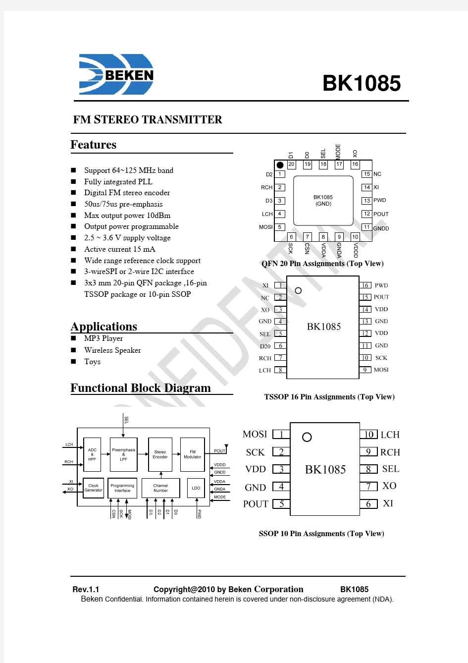
? ? ? ? ? ? ? ? ? ? ? Support 64~125 MHz band Fully integrated PLL Digital FM stereo encoder 50us/75us pre-emphasis Max output power 10dBm Output power programmable 2.5 ~ 3.6 V supply voltage Active current 15 mA Wide range reference clock support 3-wireSPI or 2-wire I2C interface 3x3 mm 20-pin QFN package ,16-pin TSSOP package or 10-pin SSOP
QFN 20 Pin Assignments (Top View)
Applications
? MP3 Player ? Wireless Speaker ? Toys
Functional Block Diagram
TSSOP 16 Pin Assignments (Top View)
SSOP 10 Pin Assignments (Top View)
Rev.1.1 Copyright@2010 by Beken Corporation BK1085 Beken Confidential. Information contained herein is covered under non-disclosure agreement (NDA).
BK1085
1 Table of Contents
1 2 Table of Contents.................................................................................................................. 2 Functional Description ......................................................................................................... 3 2.1 Power Supply ...................................................................................................... 3 2.2 Power Down and Reset ....................................................................................... 3 2.3 Pre-emphasis ....................................................................................................... 3 2.4 Stereo Encoder .................................................................................................... 3 2.5 Channel Number ................................................................................................. 3 2.6 FM modulator ..................................................................................................... 4 2.7 Reference Clock .................................................................................................. 4 2.8 Programming Interface ....................................................................................... 4 2.8.1 3-wire bus mode.............................................................................................. 4 2.8.2 I2C bus mode .................................................................................................. 4 3 Design Specification............................................................................................................. 6 3.1 Recommended Operating Conditions ................................................................. 6 3.2 DC Electrical Specification................................................................................. 6 3.3 Transmitter Characteristics ................................................................................. 6 4 Register definition1,5 ............................................................................................................. 7 5 Pin Descriptions.................................................................................................................. 10 6 Typical Application Schematic .......................................................................................... 13 7 Package Information........................................................................................................... 15 8 Order Information ............................................................................................................... 18 9 Additional Reference Resource ........................................................................................ 19 10 Revision History.................................................................................................................. 20?
Rev.1.1
Proprietary and Confidential
Page 2 of 20
BK1085
2 Functional Description
SEL
Figure1. Functional Block Diagram
CSN
SCK
MOSI
D3
D2
D1
D0
PWD
2.1 Power Supply
The BK1085 integrated a regulator which supplies power to the chip. The external supply voltage range is 2.5- 3.6 V.
2.4 Stereo Encoder
The stereo encoder is based on signal processing to encode analog stereo audio input signal and generate a composite FM signal with main, sub and pilot signal from the reference clock.
2.2 Power Down and Reset
BK1085 has already integrated the power on reset circuit inside. The chip power on/down is controlled by programming or pin PWD.
2.5 Channel Number
The BK1085 can select different channel frequency through setting the high level or low level of the channel selection pins. This function is only full available for QFN package chips.
2.3 Pre-emphasis
Pre-emphasis time constant: 50us/75us, it can be selected through SEL pin (0: 50 us, 1: 75 us).
Rev.1.1
Proprietary and Confidential
Page 3 of 20
BK1085
Table 1 [D3, D2, D1, D0] mapping to channel frequency
Channel selection bits 0 1 2 3 4 5 6 7
Channel Frequency (MHz) 87.7 87.9 88.1 88.3 88.5 88.7 88.9 From register
Channel selection bits 8 9 10 11 12 13 14 15
Channel Frequency (MHz) 106.7 106.9 107.1 107.3 107.5 107.7 107.9 From register
2.8.1 3-wire bus mode
2.6 FM modulator
The FM transmitter uses direct frequency synthesis to radiate FM wave to the air by modulating the carrier signal with the composite signal.
2.7 Reference Clock
The BK1085 accepts wide range, from 32.768 kHz to 38.4 MHz, reference clock input to the XI pin. For frequency less than 4 MHz, it must be multiplier of 32.768 KHz. The BK1085 also support crystal oscillator, using XI and XO pins. .
When selecting 3-wire mode, user must set MODE = 1. 3-wire bus mode uses SCK, MOSI and CSN pins. A transaction begins when user drives CSN low. Next, user drives an 8-bit command serially on MOSI, which is captured by BK1085 on rising edges of SCK. The command consists of a 7-bit start register address, followed by a read/write bit (read = 1, write = 0).
2.8.2 I2C bus mode
When selecting I2C mode, user must set MODE = 0. I2C bus mode only uses SCK and MOSI pins. A transaction begins with the start condition, which occurs when MOSI falls while SCK is high. Next, user drivers an 8-bit device ID serially on MOSI, which is captured by BK1085 at the rising edge of SCK. The device ID of BK1085 is 0x1D. After driving the device ID, user drives an 8-bit control word on MOSI. The control word consists of a 7-bit start register address, followed by a read/write bit (read = 1, write = 0). For I2C host reading, the host must give an ACK to BK1085 after each byte access, and should give a NACK to BK1085 after last byte read out.
Page 4 of 20
2.8 Programming Interface
The BK1085 supports both 2-wire I2C (MODE=0) and 3-wire SPI (MODE=1) programming interface. Interface clock rate can be up to 20MHz. BK1085 always latches data at the SCK rising edge and outputs its data at SCK falling edge. For MCU, data should be always written at the falling edge of SCK, and read out at the rising edge of SCK.
Rev.1.1
Proprietary and Confidential
BK1085
Command
Data[Addr]
Data[Addr+1]
Data[Addr+N]
0.5TCLK
MOSI SCK
Addr[6:0] + R/W
D[15], D[14],
, D[0]
D[15:0]
D[15:0]
CSN
0.5TCLK
0.5TCLK
Figure 2 3-wire control interface timing diagram
Device ID
ACK
Addr + R/W
Data[Addr] High Byte
0.5TCLK
A C K
Data[Addr] Low Byte
Data[Addr+N] A Data[Addr+N] High Byte Low Byte C
K
N A C K
DeviceID
Addr[6:0] + R/W
D[15:8]
D[7:0]
D[15:8]
D[7:0]
. 0.5TCLK
0.5TCLK
Start
Stop
Figure 3 2-wire control interface timing diagram
Rev.1.1
Proprietary and Confidential
Page 5 of 20
BK1085
3 Design Specification
3.1 Recommended Operating Conditions
Table 2 Recommended Operating Conditions
Parameter Analog Supply Voltage Digital Supply Voltage1 Interface Voltage Range Supply Current Audio input level Ambient Temperature
Symbol Min Typ Max Unit VA VD VIO IA VIN-A Tamb 2.5 2.5 2.5 200 -40 15 27 3.3 3.3 3.6 3.6 3.6 -10 15k 85 V V V mA dBV Hz ℃
Audio input frequency range fIN-A
3.2 DC Electrical Specification
Table 3 Absolute Maximum Ratings
Parameter Input Voltage
Symbol Min Typ Max Unit VIN -55 7 125 V ℃
Ambient Temperature Tamb
3.3 Transmitter Characteristics
Table 4 Transmitter Characteristics
Parameter Frequency range Output power Pre-emphasis time constant Audio SINAD
Test Condition
Min 64 -16 -
50us, 75us Mono 22.5 kHz Deviation
Typ 50,75 58
Max Unit 125 MHz 101 dBm us dB
Stereo separation 36 dB L/R channel balance +/- 0.5 dB Notes: 1: Measured at 50 ohm loading ,and high output power configuration
Rev.1.1
Proprietary and Confidential
Page 6 of 20
BK1085
4 Register definition1,5
Register 00h. ChanLSB (WR)
BIT [15:0] NAME FL[15:0] DEFAULT 0x86db DESCRIPTION
LSB 16 bits of frequency setting Frequency = {FH, FL}*3.8/2^21 Default frequency is 87.7 MHz
Register 01h. ChanMSB (WR)
BIT [15:0] NAME FH[15:0] DEFAULT 0x02e2 DESCRIPTION
MSB 16 bits of frequency setting Used together with FL to program channel
Register 02h. Configuration1 (WR)
BIT [15:13] [12] [11] [10] [9:4] [3:0] NAME GAIN[2:0] BYP_EM RESERVED MONO AUD_DEV[5:0] PILOT_DEV[3:0] DEFAULT 1 0 0 0 2e 3 DESCRIPTION
Digital Gain Control 1 to 1.875 , 0.125/step
Bypass Pre-emphasis Filter 0: Enable filter 1: Bypass filter Reserved Do not write anyway Mono or Stereo Selection 0: Stereo 1: Mono
Audio Deviation Adjust Default is 75kHz2 Pilot Deviation Adjust Default is 7.5kHz
Rev.1.1
Proprietary and Confidential
Page 7 of 20
BK1085
Register 03h. Configuration2 (WR)
BIT [15:4] [3:0] NAME RESERVED POUT[3:0] DEFAULT 0 7 DESCRIPTION Reserved Do not write anyway
Output Power Control3,4 0: -16 dBm; 1: -10 dBm; 3: -5 dBm; 7: 0 dBm
Register 04h/05h. Configuration3 (W)
BIT [31:28] [27:26] [25] [24] [23] [22:20] NAME PA_LOAD[3:0] RESERVED PWD_PLL PWD_PA RESERVED MICGAIN[2:0] DEFAULT 0x8 0 0 0 0 DESCRIPTION PA Load Adjust Reserved Do not write anyway
Power down PLL 0 : Power on; 1: Power down Power down PA 0: Power on; 1: Power down Reserved Do not write anyway Microphone Gain Control 0: 0dB 1: 2dB 2: 4dB 3: 6dB 4: 8 dB 5: 10dB 6: 12 dB 7: 14dB
[19:18] [17] [16:10] [9] [8:6] [5] [4] [3:2]
RESREVED XTALRESEN RESREVED RESERVED RESERVED PWD_AUD PWD_ADC RESERVED
0x3 0x1 0x04 0 0x3 0 0 0
Reserved. Do not write anyway XTAL Resistor Enable 0: Disable, for crystal frequency lower than 4M 1: Enable, for crystal frequency higher than 4M Reserved. Do not write anyway Reserved. Do not write anyway Reserved. Do not write anyway
Power Down Audio 0: Power on; 1: Power down Power Down ADC 0: Power on; 1: Power down Reserved Do not write anyway
Rev.1.1
Proprietary and Confidential
Page 8 of 20
