一种新型智能低噪声块下变频器实现的交互式通信系统(IJITCS-V10-N7-5)

I.J. Information Technology and Computer Science, 2018, 7, 39-52
Published Online July 2018 in MECS (https://www.360docs.net/doc/4414709486.html,/)
DOI: 10.5815/ijitcs.2018.07.05
A Novel Interactive Communication System
Realization through Smart Low Noise
Block Downconverter
Krishn Kumar Gupt
Institute of Informatics and Communication, University of Delhi, Delhi, India
E-mail: kumarkrishna9415@https://www.360docs.net/doc/4414709486.html,
Received: 03 September 2016; Accepted: 06 June 2018; Published: 08 July 2018
Abstract—An interactive communication is the basic motivation behind a smart communication system, which requires simultaneous downlink and uplink feature. Smart LNB is a popular discussion which is leading towards Know Your DTH (KY-DTH). A low noise block-downconverter (LNB) is the signal receiving device used for satellite TV reception mounted on the satellite dishes. For broadcasters, this smart LNB opens the door to operate their own linear TV ecosystem and other services connected directly by satellite. This new generation Smart LNB comprises of both transmitter and receiver to provide interactive TV experiences and M2M services, unlike LNB. Having uplink and downlink capability, it enables full duplex communication leading various additional applications like live interactions; live viewing; TV servicing for 24 hours; solutions for remote monitoring; control in mission critical applications in the energy and utility sectors; natural gas monitoring; Smart grid; etc. DVB-S2 source and sink are analyzed using Agilent SystemVue platform. This paper describes the study and design of a smart low noise block downconverter (LNB) used for satellite communication, transmission in Ka band (29.5 to 30 GHz) and reception in Ku band (10.7 to 12.75 GHz). The LNB design is compromised importance characteristics like Spectrum comparison. The proposed design will result in enhancement of working lifetime of the Smart LNB system with capability to receive all signals within the range. The designed and simulated process were done using Agilent SystemVue. A summary of simulation work and result over the Smart LNB in Ka and Ku band is illustrated.
Index Terms—Smart LNB (Low Noise Block downconverter), DTH (Direct to Home), KY-DTH (Know your DTH), M2M (Machine to Machine), DVB-S2 (Digital Video Broadcasting-Satellite 2).
I.I NTRODUCTION
Concept of Smart LNB was first introduced by EUTELSAT [12], a French based satellite provider. A full duplex communication is involved since Smart LNB has both transmitter and a receiver. Leading toward live interactions; live viewing; TV servicing for 24 hours; solutions for remote monitoring; control in mission critical applications in the energy and utility sectors; natural gas monitoring; Smart Grid; M2M (Machine to Machine Communication); SCADA (Supervisory Control and Data Acquisition); IOT (Internet of Things); Connected-TV; ATM; lotteries, etc.[15], Smart LNB has great application in modern communication scenarios. Smart LNB is CSWAP enabled (CSWAP is an abbreviation of Cost reduction, Size reduction, Weight reduction and Power reduction). Smart LNB overcomes the present technologies like cellular, fiber optics and existing VSAT technologies which are not CSWAP enabled and it is very hard to maintain. It allows TV platform operators and broadcasters to deploy interactive applications to their own network of Television services and linear TV connected directly via satellite. Smart LNB provides low latency and is based on iterative successive cancellation method, overcoming collisions in the communication channel. Optimized for message and burst type traffic on return link, smart LNB provides transmission and reception through bidirectional narrowband channel. Providing very high efficiency of spectrum for modulation and asynchronous access transmission protocol, it has specific band of communication. It has reception in Ku-band and return link in Ka-band or Ku-band, depending on the model. This paper describes the uses and applications of Smart LNB in interactive communication considering security, easy accessibility and to tackle the shortcomings of LNB. The aim of this research work is to develop and simulate a part of smart LNB on Agilent SystemVue, used for transmission in Ka band (29.5 to 30 GHz) and reception in Ku band (10.7 to 12.75 GHz).
II.R ELATED W ORKS
A satellite covers one third of the world. In comparison with other technologies involving communication cost per bit is the lowest in Smart LN
B satellite communication. In the coming future, there will be a competition among different modes of communication
such as cellular communication, satellite communication, Wi-Fi based communication etc. Among all these methods, Smart LNB will be in demand as the cost per bit is lowest in Satellite communication. Therefore, one of the major application of Digital Communication will be satellite communication.
Concept for SMART LNB was first introduced by EUTELSAT at Europe. And as an Industrial partner, Ayecka is presently implementing such projects [12]. This next generation Interactive Satellite terminal smart LNB is the most integrated and advanced Customer Premises Equipment (CPE). Powered by Ayecka’s RFModem technology and in partnership with Eutelsat, smart LNB opens the door for broadcasters and users. For interactive applications, this new generation smart LNB is connected to a transmitter embedded antenna. Which enables it to be use popularly in various interactive applications like social networking, HbbTV, personal subscription management, Pay-per-view and live show participations like voting, conferences, comments etc. Compared to any other solution the technology involved in Smart LNB provides exceptional bandwidth utilization [2]. Smart LNB has Ku reception (10.7-12.75 GHz, dual band) for Broadcast Data and TV signals, and Ka Transmission (29.5 - 30GHz) for Transactional-Message-based Random traffic profile for large networks [3]. The technology is adapted for low cost with highly effective network availability. SM1 involves two-way communication. ST1 and SR1 involves transmission part and the receiving part respectively [4].
Ayecka Communication Systems ltd has developed a modem SM1 in which the traffic is through Ethernet. Here IP/ETH part will be present. A virtual path with the technique of storing the packets and forwarding the packets are involved [5]. An extended version of DVB-S2, DVB-S2X provides additional specifications and technologies like Direct to Home (DTH), contribution, VSAT and DSNG [7-8]. These features can cover the emerging markets like mobile application via its extended operation range [6,11]. This leads to various applications which is affordable with a highly efficient system and highly reliable solution leading to a new area in Electronics and Communication. Low-noise block downconverter mounted on satellite dishes is the receiving device, is used for satellite TV reception. For TV signal transmission, high radio frequencies are used by satellites. As these high frequency microwaves do not easily pass through roofs, walls, dense areas and windows etc., satellite antennas are mounted outdoors. Low noise amplifier, frequency mixer, local oscillator and IF (intermediate frequency) amplifier [9] are the basis constituents of an LNB. The microwave signal from satellite is received by LNB, amplifies, and down-converts the frequency block to lower block of IF. Down converted signal can be easily carried out to indoor DTH receiver by relatively cheap coaxial cable. Unlike LNB, smart LNB involves both transmitter and receiver. Thus, a full duplex communication leads to an interactive communication technique. It provides low latency and is based on iterative successive cancellation method, overcoming collisions in the communication channel.
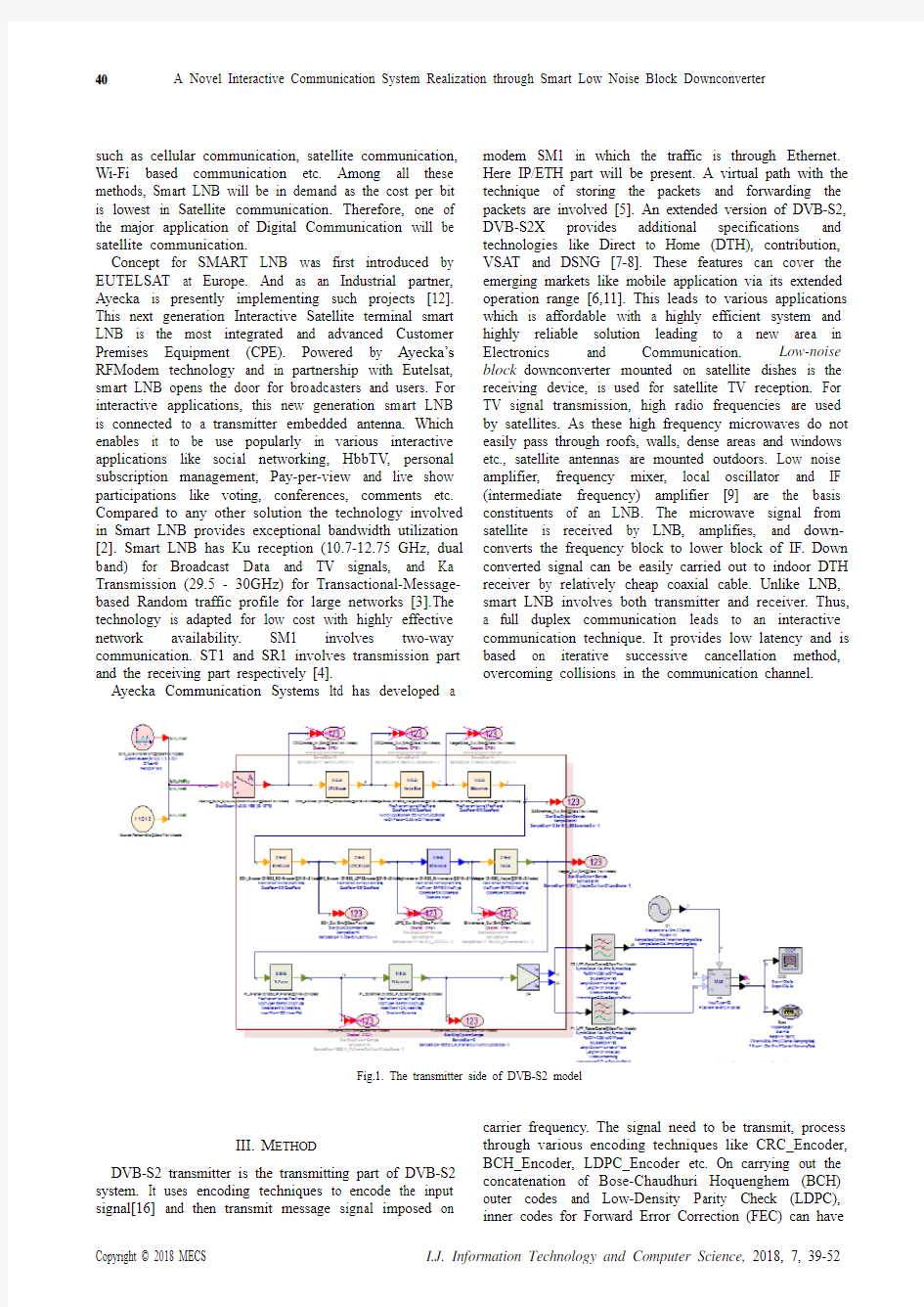
Fig.1. The transmitter side of DVB-S2 model
III.M ETHOD
DVB-S2 transmitter is the transmitting part of DVB-S2 system. It uses encoding techniques to encode the input signal[16] and then transmit message signal imposed on carrier frequency. The signal need to be transmit, process through various encoding techniques like CRC_Encoder, BCH_Encoder, LDPC_Encoder etc. On carrying out the concatenation of Bose-Chaudhuri Hoquenghem (BCH) outer codes and Low-Density Parity Check (LDPC), inner codes for Forward Error Correction (FEC) can have
the code rate 1/4, 1/3, 2/5, 1/2, 3/5, 2/3, 3/4, 4/5, 5/6, 8/9, 9/10. And for normal frame length, the Forward Error Correction (FEC) coded block length is n ldpc = 64,800 bits or 16,200 bits for short frame length depending upon the application area.
The receiver side of DVBS2 is the complement of the transmitter side. DVB-S2 is a single, very flexible standard, covering a variety of applications by satellite [2].
Fig.2. Source and Sync byte
The Source contains video, song or your message signal. Basically, the source is a like a camera. The Sync_byte consists the first byte 47HEX i.e. 01000111. After 47H the video signal follows. The purpose of the Sync_byte is for identification and synchronization purpose. A user has a full access to show the video signal or not. Depending upon the study of the signals, camera can be turned off or on by the user. Hence there is no signal after 47Hex in figure. This means that the user has turned off the source. Similarly, in other cases user can make all video signal as 1.
Fig.3. Graph obtained after Asynchronous commutator
This helps an engineer to study the signals more clearly. The Sync byte and the video signal is then passed through an Asynchronous commutator.
The graph
obtained by connecting a sink after the Asynchronous commutator obtained is shown above highlighting the first eight bits representing 47Hex.
IV.R ESULT
The Packetized Input Stream of MergerSlicer is obtained at the output with byte shift. The output of the MergerSlicer contains shifts in byte: 47 Hex to the right by addition of 80 bits in front of 47 Hex. This is done for identification and for synchronization purpose. The 80 bits circled in red and 8 bits (47Hex) circled in blue, are making a total of 88 bits. Output to MergerSlicer, find out that the header bits i.e. 88 bits, repeated after 57492 samples obtained is shown with zoom in is shown in fig.4.
Fig.4. Output of merger slicer Fig.5. The circled part zoomed In
A. Output of BB SCRAMBLER
Synchronously randomized BBFRAME from DVBS2 MergerSlicer starting from MSB to Kbch is applied in order to use Base-Band Scrambler. Scrambling is done for security purpose. The output of BB scrambler follows a simple XOR operation.
Fig.6. BB scrambler output
The possible implementation of Pseudo Random Binary Sequence (PRBS) generated by the feed-back shift register of the figure illustrates how the 15-bit PRBS pattern (100101010000000) looks like as a waveform. Loading of these sequences, shifting and Randomised BBFRAME output is shown.
Fig.7. The possible implementation of PRBS sequences
B. BCH output and LDPC Encoder
BBFrame consists of 88-bit header and video signal. Scrambling code is the convolution code as this code will be convoluted with the security code in order to be prevented by reach of hackers. Therefore, the security of the system is preserved. The output graph of the BCH is followed by BCHFEC and LDPCFEC consisting 88 bits’ header and video signal. After BBframe, BCHFEC and LDPCFEC is added to the end. BCHFEC and LDPCFEC is present at the receiving side for verifying intelligently
that whether the correct message has been delivered or not. BCHFEC and LDPCFEC can be considered like teachers who corrects the information and retains the data. This BCHFEC and LDPCFEC helps for error correction in Bit stream and required to be sent along with data separately as extended Parity Bits. After proper decoding of these two helps (BCHFEC and LDPCFEC), the receiver will be enriched with the intelligence and finally the self-correction errors would be initiated [4]. The LDPC code in the model is 8/9.
Table 1. Coding parameters for normal FECFRAME nldpc= 64,800
Fig.8. Calculated parameter
Therefore, using the values from table 1, given above the parameters Nbch, Kldpc, Kbch, Nbch-Kbch, nldpc - Kldpc are calculated as shown in the fig 8. The output from BCH output (in red) and BBscrambler output (in blue), shown in figure 09, is found to be same till 57471 (till the circled part) and represents the BBFrame.
Fig.9. Output of BCH output and BBscrambler output
From 57472 onwards the output of BCH and BBscrambler is not the same. Therefore, from 57472 to 57600 represents BCHFEC (128 bits). LDPCFEC covers
7200 bits.
Fig.10. BCHFEC = 128 bits
Fig.11. LDPCFEC
The BCHFEC and LDPCFEC covering 128 bits and 7200 bits respectively, and Output of BCH output and BBscrambler output shown above can be connected in figure8 for reference purpose. C. BitInterlever and Mapper
The BitInterlever model is to implement the bit level interlever or deinterleaver for 8PSK, 16APSK, and 32APSK modulation formats. The interleaver is disabled
in case of QPSK [17], and the output is directly connected with the input. Each firing, N ldpc bits output tokens are generated and N
ldpc
bits input tokens consumed. A mapper is present in the block diagram of the transmitter of the DVBS2. The color change of the arrows can be seen from yellow to green, representing bits to symbols conversion as seen in the figure 12.
Fig.12. DVB-S2 Mapper
FEC frame is Normal. The modulation type is 16APSK.
The code rate is 8/9. Thus, the BBframe, BCHFEC and
LDPCFEC comprises of 64, 800 bits as shown in
figure 14 [2]. For 16APSK modulation, input bits are
64,800 bits. The output symbols are given by 64800/4 =
16200 symbols, as shown in figure13. The above graph is
the input of the mapper which has 64,800 bits. After
conversion by the mapper we should get 16200 symbols
at the output.
Fig.13. 16200 symbols at the output of the mapper. After 16200 symbols, there is no signal
D. PL Framer and PL Scrambler
As shown in the figure14, the PLFraming sub-system
shall generate a physical layer frame i.e. PLFRAME.
PLFRAME generation goes through PLHEADER
insertion before XFECFRAME, followed by the
PLHEADER generation for receiver configuration. And
PLHEADER occupies here one SLOT with length M=90
symbols [10]. To help receiver synchronization, Pilot
Block insertion (for modes requiring pilots) occurs at
every 16 SLOTS with a composition of P = 36 pilot
symbols [3,10]. The output of the graph is divided into
two parts as shown in figure15 and figure16. The first
graph is based on 90 symbols PHHEADER with 16 slots
selected 8PSK modulation on random data and the
second graph is based on 90 symbols PHHEADER with
16 slots selected 8PSK modulation on data =0.
Fig.14. Format of a "Physical Layer Frame" PLFRAME
Fig.15. 90 symbols PHHEADER with 16 slots selected 8PSK modulation on random data
Fig.16. Graph: 90 symbols PHHEADER with 16 slots selected 8PSK modulation on data =0.
The model is used to implement the physical framer scrambler or descrambler as shown in figure15. Real and modulation part after SCRAMBLER with DATA= RANDOM DATA as shown in figure 18 is mentioned.
Fig.17. PL Scrambling
Fig.18. Real and modulation part after scrambler with data= random data
E. RF Level and Output spectrum
RF level and the spectrum analyzer together give the spectrum analysis of the RF signal over the smart LNB used for transmission in simulation. Double CxToRec (Complex to Real and Imaginary converter) converts RF signal into constituent parts followed by Low pass window-based linear phase FIR filter. Using Window design method, a linear-phase Low pass FIR filter is implemented by the LPF_Filter. An Interpolation number of sample is produced at output with Decimal number of sample consumption from input in each execution. Sample produced at LPF_Filter is modulated imposing 1e+09 Hz of carrier frequency. Output to the RF signal is analyzed at LPF_Filter and RF output od modulator via Spectrum analyzer. Spectrum comparison before and after LPF_Filter and analysis after modulator with carrier frequency of 1e+09 Hz, is obtained at RF level.
Fig.19. RF block with two low pass filter and modulator with 1e+9 Hz carrier frequency
Fig.20. Spectrum comparison between before low pass filter and after low pass filter Fig.21. Spectrum observer after modulator with carrier frequency of 1e+9 Hz
Figure21 at the output of spectrum analyzer gives the spectrum after modulator with carrier frequency of 1e+9 Hz. Spectrum comparison at LPF and spectrum with carrier frequency lead to quantify the data carrying channel and rate of error in data string. Applying I and Q signal respectively at the input1 and input2 in I/Q modulator, the output signal is given by[13,14]:
cx = S a (input1 + j·input2) (1) Coherent demodulator implementing I/Q demodulation reads one input sample and write one sample to output. Setting OutputType to I/Q,
output1= S a.I(t) (2)
output2=S p.Q(t) (3) ka-band(29.5GHz) frequency is used in transmission while for the reception part ku band(10.7GHz) frequency has been used.
Fig.22. RF LEVEL” 29.5GHz and 10.7GHz
Oscillator produces the carrier frequency of 29.5 GHz. In the modulation block 29.5 GHz is present for the transmission part. Further, 10.7GHz is shown in the Demodulation block for the reception part.
Fig.23. BER value = 5.708e-3
B1_BER is the BER value of first part of communication from lab 1 to lab 2 and B2_BER is the BER value of second part of communication from lab 2 to lab 1. Both the BER values are same I.e. 5.708e-3.
Fig.24. RF LEVEL with channel
“Vehicular A” environment is selected in channel. The Path Loss model for vehicular test environment is,
L=[40(1?4×10³ Δ?b)]logR?18logΔ?b+21logf+80
(4) where, R is the propagation distance in km and f is the frequency in MHz, and Δ?b is the height between base station antenna and mobile and it is set to 15 [13,14]. White Gaussian noise is added by setting the NDensityType to Constant noise density. In NDensity parameter, noise density has been specified and the unit for this parameter is power per frequency unit (Hz). Where,
Total noise power added to input signal =
NDensity × BW
(5) The noise power spectral density (NDensity) is in Watts/Hz.
Fig.25. BER level after addition of noise
The channel is added in the system so that to vary the BER in the receiver section. This varied BER will be the input of the decision block which will vary the power level according to the adjusted BER.
After addition of channel with parameters of “Vehicular_A” and noise density as 7e-9 W; BER value is varied to 0.497
V.C ONCLUSION
In this paper, smart LNB design solutions are analyzed based on approximate computing paradigm. It is shown how, the smart LNB has stimulated interesting research from transmitter, channel to receiver on a complete software-based system. We have chosen the DVBS-2 transmitter and receiver model from SystemVue to analyze the performance of smart LNB. Smart LNB is used for transmission in Ka band (29.5 to 30 GHz) and reception in Ku band (10.7 to 12.75 GHz). Realization of smart LNB, method and efficiency has been discussed through designing and simulation of model on Keysight (Agilent) SystemVue. Capability of Smart LNB over high band is simulated ensuring that it can receive all signals within the range. Spectrum analysis and comparison of signal imposed on carrier is done. An approximate computing is envisioned as an effective way to get better signal to noise ratio in smart LNB communication system. The BER (Bit Error Ratio) is found out to be 5.708e-3 with SNR (Sound to Noise Ratio) value 5. We have considered the situation in which “Vehicular A” environment is part of the channel with some path loss
and affected by noise density as 7e-9 W, we have shown
how bit error ratio is varied to 0.497 without an effective impact on system’s output quality.
A CKNOWLEDGMENT
The authors wish to thank Prof (Dr.) R. Bera, under guidance of whom he learned lot of things during his previous research work, and also for providing some notes which were useful in completing this work.
R EFERENCES
[1]ETSI EN 301 192: "Digital Video Broadcasting (DVB);
DVB specification for data broadcasting".
[2]ETSI TS 102 606-1 (V1.2.1): "Digital Video Broadcasting
(DVB); Generic Stream Encapsulation (GSE); Part 1: Protocol".
[3]ETSI EN 302 307 (V1.1.1): "Digital Video Broadcasting
(DVB); Second generation framing structure, channel coding and modulation systems for Broadcasting, Interactive Services, News Gathering and other broadband satellite applications".
[4]ETSI TR 102 376-1: "Digital Video Broadcasting (DVB)
Implementation guidelines for the second-generation system for Broadcasting, Interactive Services, News Gathering and other broadband satellite applications; Part 1: DVB-S2".
[5]https://https://www.360docs.net/doc/4414709486.html,/files/contributed/news/media_li
brary/brochures/EUTELSAT_SATELLITE_HOTBIRD_
%20Enriched_Viewing_Experience.pdf
[6]https://www.360docs.net/doc/4414709486.html,/products-smart-lnb.php
[7]https://https://www.360docs.net/doc/4414709486.html,/news/dvb_s2x-garners-market-
momentum
[8]https://www.360docs.net/doc/4414709486.html,/doi/10.1002/sat.1157/full
[9]https://www.360docs.net/doc/4414709486.html,/info/rf-technology-
design/superheterodyne-radio-receiver/block-diagram.php [10]ETSI EN 302 307 (V1.3.1): "Digital Video Broadcasting
(DVB); Second generation framing structure, channel coding and modulation systems for Broadcasting, Interactive Services, News Gathering and other broadband satellite applications (DVB-S2) ".
[11]https://https://www.360docs.net/doc/4414709486.html,/resources/public/factsheets/dvb-
s2x_factsheet.pdf
[12]Gupt, K. K., Bera, R., Bhaskar, D., Chettri, P., & Bose, D.
Smart Home realization through Wireless communication system, International Journal of Computer Science Engineering, Vol. 5, No.5, pp.240-253, Sep 2016. [13]Rec. ITU-R M.1225, Guidelines for Evaluation Of Radio
Transmission Technologies For IMT-2000, 1997.
[14]3GPP TS 36.104 v8.1.0, User Equipment (UE) radio
transmission and reception, 2008-03.
[15]Arcidiacono A, Finocchiaro D, Collard F, Scalise S,
Lazaro Blasco F, De Gaudenzi R, Cioni S, Alagha N, Andrenacci M. From S‐MIM to F‐SIM: making satellite interactivity affordable at Ku and Ka‐band, Int.
Journal of Satellite Communications and Networking 2016; 34(4):575–601
[16]P. Savvopoulos, N. Papandreou, and T. Antonakopoulos,
“The archi-tecture of a software radio DVB-S2 receiver,”
In Proc. 13th Ka and Broadband Communications Conference, Turin, Italy, Sep. 2007
[17]Soumyasree Bera, Samarendra Nath Sur,"DVBS2 System
Using SDR in Hardware-inLoop Mode", International Journal of Wireless and Microwave Technologies(IJWMT), Vol.7, No.2, pp.35-43, 2017.DOI:
10.5815/ijwmt.2017.02.04 Authors’ Profiles
Krishn Kumar Gupt, obtained his BSc
(Hons) in Electronics from University of
Delhi in 2017. He is currently doing MSc
in Informatics from University of Delhi. He
was a Summer Research Fellow under
Indian Academy Sciences, B angalore. His
area of interest is signal processing and wireless communication. He has previously done research work on topics which
are related to these fields. He has published papers in international journals on wireless communication and radio transmission.
How to cite this paper: Krishn Kumar Gupt, "A Novel Interactive Communication System Realization through Smart Low Noise Block Downconverter", International Journal of Information Technology and Computer Science(IJITCS), Vol.10, No.7, pp.39-52, 2018. DOI: 10.5815/ijitcs.2018.07.05
智能变频调速装置控制电路解析
智能变频调速装置控制电路解析 发表时间:2018-04-18T09:45:13.787Z 来源:《电力设备》2017年第33期作者:付玉佳 [导读] 摘要:本文介绍智能变频调速装置控制电路,该电路通过一只转换开关实现工/变频运行;通过面板电位器调节频率改变电机转速,调节抽油机冲次,实现简单快捷地调整抽油机参数的功能。 (大庆油田第三采油厂第一油矿) 摘要:本文介绍智能变频调速装置控制电路,该电路通过一只转换开关实现工/变频运行;通过面板电位器调节频率改变电机转速,调节抽油机冲次,实现简单快捷地调整抽油机参数的功能。该电路有工/变频两套各自独立保护系统:变频运行保护系统是通过变频器故障输出端子监测报警输出;工频保护系统通过热继电器来检测设备运行的平稳性,对电动机实现断相保护、过载保护功能,可在机采井控制领域内广泛推广。 一、现场实物图: 智能变频调速装置控制电路现场实物图 二、原理图: 智能变频调速装置控制电路原理图 三、工作原理: 1.闭合总电源及进行参数设置 (1)闭合总电源【QF1】,变频器输入端R、S、T上电,根据参数表设置变频器参数; (2)闭合控制电源【QF2】,经控制变压器TC提供控制回路220V电源,HL1电源指示灯亮。 2.工频启动与停止 (1)工频启动:将工/变频转换开关【SA】转至工频位置,端子③→④接通,按下工频启动按钮【SB3】,回路经1→7→8→9→10→11→0闭合,KM1线圈得电,回路8→9线间KM1常开触点闭合自锁,控制回路中2→3线间KM1常闭触点断开,断开变频控制回路,与KM2接触器实现机械联锁。同时主回路中KM1主触头闭合,电动机工频运行,回路1→12线间KM1常开触点闭合,KM3线圈得电,强制风机运行,工频运行指示灯HL2亮。 (2)工频停止:按下停止按钮【SB1】,回路7→8断开,KM1线圈失电,回路8→9线间KM1常开触点断开,回路2→3线间KM1常闭触点复位,回路1→12线间KM1常开触点断开,KM3线圈失电,强制风机停止,同时KM1主触头断开,电动机停止运行,工频运行指示灯HL2熄灭。 3.变频启动与停止 (1)变频启动:将工/变频转换开关【SA】转至变频位置,端子①→②接通,按下启动按钮【SB2】,回路经1→4→5→6→0闭合,KA、KT1、KT2线圈得电,回路5→6线间中间继电器KA常开触点闭合自锁,回路1→2线中间继电器KA常开触点闭合,经回路1→2→3→0闭合,变频接触器KM2线圈得电,主触头闭合,电动机开始运行,回路1→12线间KM2常开触点闭合,风扇接触器KM3线圈得电,强制散热风扇运行,同时回路9→10线间KM2常闭触点断开,与KM1接触器实现机械联锁。当时间继电器1延时时间到达后,回路13→14线间KT1延时闭合常开触点短接变频器输入端子[DINI]与公共端端子[COM],变频器正转输出,操作面板【正转】、【RUN】指示灯亮,频率数值由电位器给定,同时回路1→2线间时间继电器KT2延时断开瞬时闭合触点闭合,变频运行指示灯HL2亮。 变频调速:该变频器调速控制采用面板电位器调速,顺时针旋转电位器钮频率上升电动机加速,逆时针旋转电位器钮频率下降电动机减速,频率数值在面板七段数码管上显示。 (2)变频停止:按下停止按钮【SB1】,回路4→5断开,中间继电器KA、时间继电器KT1、KT2线圈失电,回路中5→6线间KA的常开触点断开,回路1→2线间中间继电器KA常开触点断开,时间继电器KT2断电延时,延时断开触点保持,变频运行指示灯HL2保持,回路经2→3线间工频接触器KM1常闭触点变频接触器KM2线圈保持,KM2主触头保持变器输出端子与电动机输出端子的连接,回路13→14线间时间继电器KT1延时闭合瞬时断开触点断开,变频器[DINI]端子与[COM]端子断开,操作面板【正转】、【RUN】指示灯熄灭,【STOP】指示灯亮,频率数值开始下降,电动机转速下降,电动机轴上的机械能通过电动机转换成再生电能,经变频器[PB]与[P]端子之间的外置直
一种新型直接抽取算法的数字下变频设计
一种新型直接抽取算法的数字下变频设计 【摘要】为了简化卫星导航接收机框架,提出一种基于数字信号抽取的下变频方法。通过分离和累计法,人们发现了一种具有高频率数字载波信号的直接下变频方法。这种方法不仅具有结构简单、速度高和计算简单的特点,还能够很好的保持导航电文和多普勒信息,但这种方法有可能会使S/N信号和接收机的灵敏度降低:分析和仿真结果显示,它对接收机的定位灵敏度没有任何的影响。 【关键词】数字下变频;抽取算法;BPSK 1.引言 卫星导航接收机通常采用超外差的体系结构,在模拟的超外差接收机前端,许多的数字下变频是通过使用混频器和本地振荡器接收IF信号。低通滤波器消除了高频率分量,然后便可以得到不同频率的下变频信号,与低IF模式和零IF 模式相比,它具有高增益、高抑制和无本地振荡泄漏的特点,但是它的结构复杂和功率损耗较高[2]。 数字接收器具有高集成度、低功耗和低成本的特点,因此,它是无线电接收器的发展趋势[3]。数字下变频方法能够通过数字调音台、CIC滤波器或者重采样方法把一个高频率信号转变成低频率信号[4-5]。在本文中,抽取算法和提取信号是为了得到BPSK调制信号的下变频,与CORDIC方法相比,数字下变频方法只需要添加点操作就可以节省许多的时间和CPU空间。在处理导航数据或CDMA数据时,除了采样IF算法外,还需要重采样和复杂的数字算法。 2.抽取算法的原理 假设在模数转换之前,信号的频率为,抽样频率是。对于BPSK调制的信号,载波频率和振幅是不变的。经过A/D转换后,信号为是一个行向量,向量的位数等于A/D转换器的位数。无相位转换的载波抽样信号有如下关系: 如果相位在周期发生转换,并且是在和周期之间发生,由于相位变化是,最后的抽样值不如前个抽样值,。如果>,在抽取的过程中相变不会发生,那么便会在下个周期发生。因此,在抽取期发生的相变将提前或推迟以适应周期的开始或结束,从而导致部分代码相位误差。 3.灵敏度和准确度的影响 抽取和量化将会造成信号信息的丢失,此量化误差是依赖于量化比特数和阀值。通过选择合适的阀值可以使量化的损失减少,通常情况下,实验中的量化是0.55dB[7]。抽取值可以改变相变的位置。如果累计的最大数目是,它可以使相位的过渡时间提前或滞后正确点的,是抽样周期。相变错误也影响相关积分结果,这会使接收器的灵敏度降低。考虑了多普勒频移,相变误差均匀分布的区域是,
变频器模拟量控制练习题
第一题搅拌机控制 有一台搅拌机,用三相交流异步电动机拖动,其控制要求如下:(1)工作过程: 当按下启动按钮SB1 时,电动机首先正向旋转5分钟,然后停2分钟,然后反向旋转5分钟,停2分钟,然后再正转……如此循环。 (2)停止过程: 任何时候,按下停止按钮SB2,电动机停止运行。 (3)电动机速度控制: 电动机由变频器驱动控制,变频器速度应用PLC模拟量给定,要求模拟量信号类型为0~20mA电流信号,电动机正向运行频率为38HZ,反向运行频率为26HZ。 电动机运行过程中,PLC用模拟量输入通道读取变频器实际运行频率值。
第二题电动机启动控制 有一台三相交流异步电动机带动大惯性机械负载,为避免启动和停止时负载冲击,需采用分段速度递增和递减的方式,其控制要求如下: (1)电动机启动: 当按下启动按钮SB1时,电动机首先以10HZ频率启动,每隔3分钟频率提高5HZ,到达最高频率50HZ后不再提高。 (2)停止过程: 按下停止按钮SB2,电动机立即减速至45HZ,然后每隔3分钟运行频率减少5HZ,运行频率降低到10HZ及以下时,电动机停止运行。 电动机由变频器驱动控制,变频器速度应用PLC模拟量给定,由变频器模拟量端子10、11引入,要求模拟量信号类型为0~ 10V电压信号。系统运行过程中PLC实时监控变频器实际运行频率和运行电流值。
某工作台由一台三相交流异步电动机拖动,在工作台运行的左右两端有限位开关,工作台可以手动运行,也能做自动往返的运行。其控制要求如下: (1)工作过程: 工作台手动运行和自动运行可以利用钥匙开关SA0 来选择。 在SA0 选择手动控制方式时,按下前进按钮SB1,工作台向右前进;按下后退按钮SB2时,工作台向左后退。 在SA0 选择自动控制方式时,按下启动按钮SB3,工作台如果不 在最左端,则应向左后退先返回最左端,碰到左端限位开关后,自动向右前进;如果工作台已经在最左端,则工作台直接向右前进。向右碰到右端限位开关后,工作台停止3分钟钟,然后向左后退,直至碰 到左端限位开关后,工作台继续向右前进……如此循环往复。 (2)停止过程: 任何时候,按下停止按钮SB4,工作台立即停止。 (3)电动机速度控制: 电动机由变频器驱动控制,电动机手动运行状态下运行频率固定 为10HZ。自动运行模式下,前进运行频率为30HZ,后退运行频率为50HZ。 变频器速度应用PLC模拟量给定,由变频器模拟量端子10、11引入,要求模拟量信号类型为0~ 20mA电流信号。系统运行过程中PLC 实时监控变频器输出电压和运行电流值。
V20变频器PID控制恒压供水操作指南(DOC)
V20变频器PID控制恒压供水操作指南 1.硬件接线 西门子基本型变频器SINAMICS V20 可应用于恒压供水系统,本文提供具体的接线及简单操作流程。 通过BOP设置固定的压力目标值,使用4~20mA管道压力反馈仪表构成的PID控制恒压供水系统的接线如下图所示: 图1-1.V20变频器用于恒压供水典型接线 2调试步骤
2.1 工厂复位 当调试变频器时,建议执行工厂复位操作: P0010 = 30 P0970 = 1 (显示50? 时按下OK按钮选择输入频率,直接转至P304进入快速调试。) 2.2 快速调试 表2-1 快速调试参数操作流程 参数功能设置 P0003 访问级别=3 (专家级) P0010 调试参数= 1 (快速调试) P0100 50 / 60 Hz 频率选择根据需要设置参数值: =0: 欧洲[kW] ,50 Hz (工厂缺省值) =1: 北美[hp] ,60 Hz P0304[0] 电机额定电压[V] 范围:10 (2000) 说明:输入的铭牌数据必须与电机接线 (星形/ 三角形)一致 P0305[0] 电机额定电流[A] 范围:0.01 (10000) 说明:输入的铭牌数据必须与电机接线 (星形/ 三角形)一致 P0307[0] 电机额定功率[kW / hp] 范围:0.01 ... 2000.0 说明:如P0100 = 0 或2 ,电机功率 单位为[kW] 如P0100 = 1 ,电机功率单位为[hp] P0308[0] 电机额定功率因数(cosφ )范围:0.000 ... 1.000 说明:此参数仅当P0100 = 0 或 2 时可见P0309[0] 电机额定效率[%] 范围:0.0 ... 99.9 说明:仅当P0100 = 1 时可见 此参数设为0 时内部计算其值。 P0310[0] 电机额定频率[Hz] 范围:12.00 ... 599.00 P0311[0] 电机额定转速[RPM] 范围:0 (40000) P0314[0] 电机极对数设置为0时内部计算其值。 P0320[0] 电机磁化电流[%] 定义相对于电机额定电流的磁化电流。 设置为0时内部计算其值。 P0335[0] 电机冷却根据实际电机冷却方式设置参数值 = 0: 自冷(工厂缺省值) = 1: 强制冷却 = 2: 自冷与内置风扇 = 3: 强制冷却与内置风扇
基于matlab的简单数字下变频器的设计
一、课程设计问题的提出: 试设计一数字下变频器,并用matlab 仿真; 二、二、解决问题的原理、技术方案解决问题的原理、技术方案解决问题的原理、技术方案以及以及matlab 验证验证: :数字下变频器的原理说明: 数字下变频器(D DC)是接收机A /D 变换后,首先要完成的处理工作,一般的DDC 由本地 振荡器(NCO)、混频器、低通滤波器和抽取器组成.主要作用:其一是把中频信号变为零中频信号;其二是降低采样率。从频谱上看,数字下变频将A/D 采样后信号从中频变换,到基带。这样的处理由两步完成:首先是将输入信号与正交载波相乘,然后进行数字滤波滤除不需要的频率分量。NCO ,混频器,数字滤波器速率要等于采样率,采样率低于600MHz ,很难实时的在FPGA 中进行处理。 数字下变频器的基本结构: NCO :产生正余弦序列,即I/Q 两路信号。 CIC 滤波器,适用于系统中的第一级抽取和进行大的抽取因子的抽取工作,并降低速率。FIR 滤波器,完成对整个信道的整形滤波。DDC 主要有三种实现途径:采用专用芯片、自制专用芯片、基于DSP 或FPGA 等通用芯片。
NCO采用的直接数字频率合成技术(DDS)是一种实用的频率合成技术,DDS由相位概念出发直接合成所需波形的一种新的频率合成技术。DDS合成技术采用了简便和有效的查表法。 运用matlab进行NCO的仿真: 程序: t=0:0.001*10^(-6):10^-6; I=110*cos(7*(10^7)*t-0.5*pi); subplot(2,1,1);plot(t,I);grid on; Q=110*sin(7*(10^7)*t+0.5*pi); subplot(2,1,2);plot(t,Q);grid on; 信号的频率为11.2MHz CIC滤波器: CIC滤波器,即级联积分梳状滤波器,具有结构简单,便于处理,运算速度快等特点。CIC 滤波器的积分器H1(Z)是不稳定系统,如果不采取措施,它们级联后会出现溢出现象。另外,
关于模拟量控制变频器的调试讲解
移位指令与模拟量控制的运用 在实际工作中,常常碰到一些例如机械手等等之类的步进控制。如果在步进控制中再参入一些检测之类的其它工作要求,按照步进指令一步一步的编写程序,将会使程序变得异常繁琐。此时如果使用移位指令来控制步进动作,则会使步骤清晰,程序之间减少了许多不必要的干扰。如果只是单纯的几个简单的气缸之类的控制,适合于用步进指令来编写程序。 下面是电机的多段速模拟量控制,使用欧姆龙PLC,(CP1H-XA型)用移位指令来编写动作步进控制程序。此程序节选自福特汽车门锁门铰链耐久测试控制系统。模仿福特汽车开门、关门动作,测试门铰链的耐久程度。 一、控制要求:如下图1-0所示。 图1-0 整体分为左门速度控制,右门速度控制两大类,它们的控制要求相同。电机速度可调,循环次数可调,可以在触摸屏上任意设置速度。多段速控制有四个要求:开门过载模式、正常循环模式、带冲击开门模式、带冲击关门模式。当整个动作的行程出现意外时,有个最大行程保护,也就是行程保护控制。 整体动作控制有两个。停止---开门---停止----关门----停止。即电机的正转,反转。多段速运行分为以下几种: 正常循环模式。模仿车门在轻轻的开门,轻轻的关门动作时,门铰链的耐久程度。在开门动作时的多段速(启动加速---正常速度---停止减速)。在关门动作时的多段速(启动速度---正常速度---停止减速)。 带冲击开门模式。模仿车门在用力的开门,轻轻的关门动作时,门铰链的耐久程度。在开门动作时的多段速(启动加速---正常速度---冲击加速)。在关门动作时的多段速(启动速度---正常速度---停止减速)。 带冲击关门模式。模仿车门在轻轻的开门,用力的关门动作时,门铰链的耐久程度。
基于希尔伯特变换法的数字下变频
基于希尔伯特变换法的数字下变频 唐雷雷 1000030028 引言 本文主要讲述了数字下变频DDC 的基本原理,分别用低通滤波法和希尔伯特变换法实现数字下变频DDC ,同时用MATLAB 做了仿真和对比。 ABSTRACT This paper describes the Digital Down Conversion (DDC )of the basic principles. The Digital Down Conversion (DDC )is implemented by a low-pass filtering and Hilbert transform method , also is simulated by MATLAB and compared. 关键词: DDC 希尔伯特变换 MATLAB 一、中频正交采样的基本原理 在信号处理领域,对接收到的信号进行正交相干检波,可以保留信号复包 络的所有信息,获得良好的正交特性,因而在雷达、声纳、通信等电子系统中得到广泛的应用[2]。 一个系统所接收到的中频信号可以表示为: 00 (2()) 2' ()() () j f t t j f t x t a t e x t e π?π +== (1) 式中, f 为中频频率,()a t 和()t ?分别表示信号的幅度和相位, ' ()()e x p ( ())()()x t a t j t I t j Q t ?==+,称为()x t 的复包络(基带信号),它包含了带 通信号的所有信息。其中 ()()()cos ()()()()sin () I Q I t x t a t t Q t x t a t t ??==== (2)
变频器注意事项
6SE70 一、O008闭锁看参数R550的状态显示 1、控制字BIT0 OFF1 P554,故障复位后启动命令P554还在,则闭锁,此时停止后 再启动,正常 2、控制字BIT1 OFF2 P555 P556 P557为0,改为1即可 3、控制字BIT2 OFF3 P558 P559 P560为0,改为1即可 4、控制字BIT3 逆变器使能P561为0则启动时会显示O011,改为1即可 5、控制字BIT4 斜坡使能P562为0则启动时速度为0.00,改为1即可 6、控制字BIT5 斜坡开始P563为0则启动时速度为0.00,改为1即可 7、控制字BIT6 设定值使能P564为0则启动时速度为0.00,改为1即可 8、控制字BIT8 点动0 (P568),P554为0时有效 9、控制字BIT9 点动1 (P569)P554为0时有效 当P568和P569同时为1时,变频器启动时显示O008,闭锁。不需要点动功能时,将两个参数设成0. 10、控制字BIT11 正转(P571) 11、控制字BIT12 反转(P572) P571和P572一个为1,一个为0,则能实现正反转;或两个都为1,则变频器直接由速度给定P443控制;如果都为0,则启动时速度为0,并报警A035 12、控制字BIT13 电位计+ (P573)P554为1时有效 13、控制字BIT14 电位计- (P574)P554为1时有效 正常时两个参数为0,当都为1时,速度为0,无法控制变频器的速度。 14、控制字BIT15 外部故障P575为0则报F035,改为1即可 一般正常启动运行的控制字显示是R550: 1 0 0 1 1 1 0 0 0 1 1 1 1 1 1 0 上例是P571=1 P572=1,反转靠速度给定。当然也可以一个为1,一个为0,但是不能都为0,否则无法给定速度,且报警A035。 二、BICO数据组切换。 P590参数切换 有可能故障出在:参数已经设置好,能够实现功能,比如网络控制,P554.1=3100,P443.1=3002(即第一套参数),但无法启动,此时看R012(BICO参数组)是否为1,如果等于2,说明P590为1,则改成0后正常。 三、故障代码 F011:过流 F021:过热 F015 F053:堵转(检查编码器) F037:变频器的模拟量输入选择了电流型,且低于下限4mA(如果选择了4—20mA)。
数字下变频仿真
数字下变频仿真原理: 信号采样的频谱 调频信号:02 ()cos *(2/2)s x K t n f nt π=+ 00022 02 *cos(2/)cos(2)cos(2) cos(4*/2*/2)cos(*/2) s s s s x f n f f nt f nt f nt K t K t K t ππππ=+=++ 0002022 *sin(2/)cos(2)sin(2) sin(*/2*/2)sin(*/24) s s s s K t K t K x f n f f nt f nt f nt t ππππ+-=-+=-+ 因为f 0=30MHz ,整体向左平移30MHz 。 -40-20 带宽为5MHz 通过仿真得到()x n 的时域波形和频域波形,如下图所示。 clc;clear all;close all; f0=30e6; 中心频率 B=5e6; 带宽 T=30e-6; 脉冲宽度 fs=40e6; 采样频率 N=T*fs; 采样点数 K=B/T; 频率变换率 ts=1/fs; 采样周期
t=-T/2:ts:T/2-ts; x=cos(2*pi*(f0*t+K*t.^2/2)); figure(1); title('时域波形'); xlabel('point '); figure(2); plot(abs(fft(x))); title('频域波形'); xlabel('point'); I路信号和Q路信号: ddc_i = x.*cos(2*pi*f0*(1:N)/fs); I路信号ddc_q = -x.*sin(2*pi*f0*(1:N)/fs); Q路信号figure(3); subplot(211); plot(t,ddc_i);grid; title('I路波形');
通信系统中的数字上变频和下变频
通信系统中的数字上变频和下变频 数字上变频器(DUC)和数字下变频器(DDC)不仅仅是通信应用(如软件无线电)中的关键,而且在需要窄带信号高速流的应用中也是重要的。另外,DDC结构容易控制所有取样速率下的混淆防止分样。 让我们看看数字记录5MHz带宽(中心在50MHz)信号的问题。此信号可以是来自RF-IF模拟下变频器的信号或者是直接从天线接收的信号。为了满足尼奎斯特准则,我们需要以 105ms/s取样率取样此信号。然而,为了合理地捕获此信号,应该在较高的取样率(至少200ms/s)取样此信号。假设ADC为16位,在该速率下被取样的信号会产生400MB/s数据。也许更难办的是以这样高速率采集和存储数据缺乏商业可用的方案。大多数可用的PC基数字器仅能在大约几分之几秒内存储此数据。 数字下变频 DDC在持续时间期间可以数字记录RF信号。在此实例中,我们仅需要记录5MHz信号(中心频率50MHz),而不是ADC的整个尼奎斯特带宽。DDC允许除去其余数据,并降低数据率。在现场可编程门阵列(FPGA)中实现时,简单的数字下变频分为3个性质不同的步:频率变换、滤波和分样(图1)。 频率变换和滤波 第1步是频率变换。5MHz频带需要降低变换到基带,靠乘或与载频(fc)正弦信号混频实现这种变换。用数字控制振荡器(NCO)数字产生正弦波。NCO通常也称之为本机振荡器(LO),它可以在精确频率和相位下产生取样波形。 随着信号从50MHz变频到基带,信号拷贝也从50 MHz变频到100 MHz。基于此原因,新的基带信号必须滤波,去除较高频率的信号。然而,到此我们的任务没有完成。我们仍有1个在200ms/s取样的低频基带信号。传输额外不必要数据时不希望PC总线过载,我们重新取样信号来降低有效取样率。这靠分样实现,在规则的时间间隔内从数字化的信号中去除数据点。在此例中,取样从200ms/s下降到10ms/s,每20个取样去除19个取样。 防止混淆的分样 采用分样,数字化器的采集引擎继续以同样的最大速率进行取样。然而,仅有少量的采集点被存储、被取出和传输到PC,这降低取样率到所希望的水平。但是,此技术不是极简单的。 为便于说明,假定数字化器的最大取样率是100MS/s,使其尼奎斯特频率为50 MHz,而信号有两个分量:10 MHz基频和20MHz激励频率分量。若数字化器分辨率为14位,则在100MS/S总数据率是200MB/s,这远远高于PCI总线理论极限132MB/s。这是采用较低取样率(如25MS/s)的1个原因。现在尼奎斯特频率应该是12.5MHz。然而,20MHz频率分量混淆回到5MHz。现在,不可能告知信号实际上是否是5MHz信号或混淆到5MHz的另外较高频率信号(20MHz,30MHz,45MHz)。 解决此问题的1种方案是称之为防止混淆分样的增强分样技术。在此技术中,数字化器继续在100MS/s最高取样率下采集数据,但加1个低通数字滤波器,在分样前截止尼奎斯特频率(图2)。 正交数字下变频 图1所示DDC只适用于单维调制信号。这种信号的1个实例是AM无线电的双边带幅度调制信号,它用比实际所需两倍的带宽。这样的信号在低和高于载频是相同的。
皮带机智能变频调速节能控制系统
皮带机智能变频调速节能控制系统 摘要随着科学的发展,皮带机的控制系统也快速的发展,将模糊控制和变频调速技术结合在一起的皮带机智能变频调速节能控制系统,在节能和性能方面,相比于以前的系统都有了很大的提升。本文结合了皮带机的控制技术以及变频调速技术的应用来对皮带机智能变频调速节能控制系统进行了研究。 关键词皮带机;变频调速;节能;控制系统;模糊控制 0 引言 随着科学的不断发展,生产系统的发展也非常迅速,从原来的比较简单的系统发展成了现在比较复杂的庞大系统。而在皮带机的控制系统中,也不断有新的技术可以让皮带机的工作更加高效更加节能,变频调速技术就是其中的一种,为了可以让皮带机的无级平滑调速得以实现,它可以通过变频器对电源的输出频率进行改编,从而任意调节电机的转速。变频调速技术有两大优点,第一是节能,第二则是调速的性能相当优越。模糊控制也是比较新的技术,本系统将模糊控制与PLC结合在一起,利用PLC来对模拟控制进行实现,这样就不仅能够让PLC 的灵活、可靠、适应性强等优点保留下来,还能够让控制系统更加的智能。 1 皮带机的模糊控制技术 1)模糊控制的原理 皮带机的模糊变频调速控制能够把观测值输入到模糊控制器当中,然后得到一个经过了一系列流程的确切控制量,分别是模糊化、模糊推理以及清晰化操作,再将其作用到被控对象之上。在多数的情形下,为了可以让在线的计算量减少,通常是采用离线计算的方式,形成一个模糊控制表,再将这个表以数据模块的形式储存在计算机的程序当中,当接收到一组输入时,能够根据模糊控制表来给出相应的输出值。这个方法能够让原本非常复杂的计算过程用查表的方法来解决,让工作变得更加高效。 设计人员并不能根据皮带机来建立一个非常准确的数学模型,主要的原因是系统存在着滞后、时变以及非线性等现象,也因为各种物料的不同,让启动的加速度也有所差异,因此在建立数学模型的时候会遇到很多困难。在这种情况下,就使用模糊控制技术来对皮带机进行控制,当主电机的电压值到了额定电压之后,变频机就可以根据之前制定的输出轴的速度曲线来对电机进行调速的工作,同时对传感器也进行利用,采集实际的速度,并将采集得到的结果与之前给定的速度相比,对误差以及误差的变化进行计算,再对其进行计算输出,这个输出值就可以输入到变频器当中,实现模糊控制。 2)模糊控制结构
PLC控制变频器转速
PLC控制变频器转速 2008-09-09 3:19 本文以三菱PLC为例介绍了模拟量控制,并结合变频调速基本原理及特点,重点阐述了如何通过PLC模拟量控制来实现对变频器的速度调节。 1、引言 近年来可编程序控制器(PLC)以及变频调速技术日益发展,性能价格比日益提高,并在机械、冶金、制造、化工、纺织等领域得以普及和应用。为满足温度、速度、流量等工艺变量的控制要求,常常要对这些模拟量进行控制,PLC模拟量控制模块的使用也日益广泛。 通常情况下,变频器的速度调节可采用键盘调节或电位器调节方式,但是,在速度要求根据工艺而变化时,仅利用上述两种方式则不能满足生产控制要求,因此,我们须利用PLC灵活编程及控制的功能,实现速度因工艺而变化,从而保证产品的合格率。 2、变频器简介 交流电动机的转速n公式为: 式中: f—频率; p—极对数; s—转差率(0~3%或0~6%)。 由转速公式可见,改变三相异步电动机电源频率,可以改变旋转磁通势的同步转速,达到调速的目的。额定频率称为基频,变频调速时,可以从基频向上调(恒功率调速),也可以从基频向下调(恒转距调速)。因此变频调速方式,比改变极对数p和转差率s两个参数简单得多。同时还具有很好的性价比、操作方便、机械特性较硬、静差率小、转速稳定性好、调速范围广等优点,因此变频调速方式拥有广阔的发展前景。 3、PLC模拟量控制在变频调速的应用 PLC包括许多的特殊功能模块,而模拟量模块则是其中的一种。它包括数模转换模块和模数转换模块。例如数模转换模块可将一定的数字量转换成对应的模拟量(电压或电流)输出,这种转换具有较高的精度。
在设计一个控制系统或对一个已有的设备进行改造时,常常会需要对电机的速度进行控制,利用PLC的模拟量控制模块的输出来对变频器实现速度控制则是一个经济而又简便的方法。 下面以三菱FX2N系列PLC为例进行说明。同时选择FX2N-2DA模拟量模块作为对变频器进行速度控制的控制信号输出。如图1所示,控制系统采用具有两路模拟量输出的模块对两个变频器进行速度控制。、 图1 对变频器进行速度控制的信号输出 图2为变频器的控制及动力部分,这里的变频器采用三菱S540型,PLC的模拟量速度控制信号由变频器的端子2、5输入。
线性调频信号脉冲压缩-数字下变频程序 DDC
线性调频信号脉冲压缩-数字下变频程序DDC clc; clear all; close all; B=5e6; %%信号带宽 f0=30e6; %中频 fs=40e6; %采样频率 fs1=(20/3)*1e6; %%抽取后频率 T=24.9e-6; %%时宽 k=B/T; fk=127; %%做DDC时的低通滤波器的阶数 fid=fopen('20090724fc1yindao4-0.dat','r'); sss=fread(fid,32*4096,'int16'); fclose(fid); figure(100);plot(sss);grid on;xlabel('点数');ylabel('幅度');title('32个周期信号时域波形');grid on; L=length(sss); N=4096; R=fix(L/N); for r=1:R ss(r,:)=sss((r-1)*N+1:1:r*N); end figure(1);plot(ss(R,:));xlabel('点数');ylabel('幅度');title('信号时域波形');grid on; %%%%%%%%%%%%%%% 低通滤波器%%%%%%%%%%%%%%%%%%%%%%%%%%%%%%%%% ff=[0 1/8 1/4 1]; aa=[1 1 0 0]; b=firpm(fk,ff,aa); [h,w]=freqz(b,1,1024); % figure(2); % f=linspace(0,fs/2,1024); % plot(f/1e6,20*log10(abs(h)));xlabel('f/Mhz');ylabel('dB');title('低通滤波器的幅频响应');grid on; %%%%%%%%%%%%%%% DDC %%%%%%%%%%%%%%%%%%%%%%%%%%%%%%%%% ddcs=zeros(R,N+fk); for r=1:1:R n=-N/2:1:N/2-1; si=ss(r,:).*cos(2*pi*f0*n/fs); sq=-ss(r,:).*sin(2*pi*f0*n/fs); I=conv(si,b);
智能变频控制技术的研究与设计
智能变频控制技术的研究与设计 摘要 随着现在电力电子技术、交流变频调速技术的飞速发展和现代控制理论,告诉微处理器的普及应用,变频调速技术以其良好的调速能力及节能特性越来越多的应用于工程实际。对于电动执行机构,采用变频调速可以省去复杂的机械齿轮组设计,实现电机的软启动和软停机。 本文首先对电动执行机构在国内外的研究现状和发展趋势进行了大量的分析,对于目前电动执行器只有以低速运行,通过极强的微调作用才能修正微小偏差的缺点,提出了智能型电动执行器与各种阀体配合,利用数字化变频技术、单片机技术、微电子技术,开发了集执行机构、驱动单元、调节控制单元等为一体的智能电动执行机构。 智能控制电路从结构上主要分为控制部分、执行驱动部分及信号检测部分。控制部分主要单片机、变频调速模块、智能功率模块、整流模块、开关量输入输出通道、故障检测电路等组成;执行驱动部分主要包括执行电机和机械传动部分;检测部分包括电压、电流、温度检测。采用直接转矩控制算法控制变频器,并在线组态,实现对执行器电机的调速控制,实现了电机柔性启动和平稳运行,避免系统对阀门的冲击。 关键词:智能电动执行器;变频控制;单片机。
Research and Design of intelligent frequency conversion control technology Abstract With power electronics technology, the rapid development of AC variable speed technology and modern control theory to tell more and more used in engineering with its good speed capacity and energy-saving features of the universal application of the microprocessor, frequency conversion technologypractical. Frequency control eliminates the need for complex mechanical gear set design for the electric actuator motor soft start and soft stop. The first electric actuator in the status quo and development trend of domestic and foreign research a lot of analysis performed for the electric actuator only drawback to running at low speed, strong fine-tune the role to correct minor deviations proposed intelligent electricwith the valve body with using digital inverter technology, single-chip technology, micro-electronics technology, developed a set of implementing agencies, the drive unit, adjust the control unit and other for the integration of intelligent electric actuators. Intelligent control circuit structure is divided into the control part of the implementation of drive parts and signal detection part. Control part of the main microcontroller, frequency control modules, intelligent power module, rectifier module, switch input and output channels, fault detection circuit; execution driven mainly include the implementation of the motor and mechanical drive components; detection part including voltage, current, temperature detection . S the use of direct torque control algorithm to control the frequency converter and online configuration, speed control actuator motor, motor soft start and smooth running, to avoid the system on the impact of the valve. Keywords: intelligent electric actuators; inverter control; microcontroller.
基于FPGA的DDC(数字下变频)设计与实现
基于FPGA的DDC(数字下变频)设计与实现
微系统设计、测试与控制 课程大作业之 基于FPGA的DDC(数字下变频) 的设计与仿真
摘要 (1) ABSTRACT (2) 第一章绪论 (3) 1.1 数字下变频(DDC)研究背景 (3) 1.2 DDC概述 (4) 1.3 本文研究内容和结构安排 (5) 第二章数字下变频(DDC)基础理论 (7) 2.1 数字下变频器 (7) 2.1.1 数字变频的基本原理与结构 (7) 2.1.2影响数字变频器性能的主要因素7 2.2 数字信号采样理论 (8) 2.2.1低通信号采样理论 (8) 2.2.2 带通信号采样理论 (9) 2.3 数字正交检波 (10) 2.3.1 低通滤波法 (10) 2.3.2 多相滤波结构变换法 (11) 2.4 多抽样率数字信号处理理论 (13)
2.4.1 整数倍抽取和内插 (13) 2.4.2 多抽样率系统的恒等变换 (16) 2.4.3 多相滤波结构 (17) 2.5 相关算法介绍 (19) 2.5.1 CORDIC算法 (19) 2.5.2 FIR滤波器 (21) 2.6 本章小结 (22) 第三章数字下变频(DDC)各模块设计 (23) 3.1 数字下变频的基本实现方案 (23) 3.2 基于DDS的数控振荡器的设计 (23) 3.2.1 混频器模块设计 (23) 3.2.2 DDS的特点 (25) 3.3抽取滤波 (27) 3.4 本章小结 (29) 第四章数字下变频器设计验证和逻辑综合 (30) 4.1基于DDS的数控振荡器的仿真和验证30 4.2 FIR滤波器的仿真和验证 (32)
基于PLC模拟量方式的变频器闭环调速
基于PLC模拟量方式的变频器闭环调速 在MF51变频器实验挂箱中完成此实验 一、实验目的 1.利用可编程控制器及其模拟量模块,通过对变频器的控制,实现电机的闭环调速。 2.了解可编程控制器在实际工业生产中的应用及可编程控制器的编程方法。 二、实验要求 变频器控制电机,电机上同轴连旋转编码器。编码器根据电机的转速变化而输出电压信号Vi1反馈到PLC模拟量模块(FX2N-4AD)的电压输入端,在PLC内部与给定量经过运算处理后,通过PLC模拟量模块(FX2N-2DA)的电压输出端输出一路DC0~+10V电压信号Vout来控制变频器的输出,达到闭环控制的目的。 三、实验原理图 四、实验步骤 1 n10 Pr.30 Pr.73 Pr.7 9 1 1 4 0 2.输入输出接线 3.按接线列表正确将导线连接完毕后,将程序下载至PLC主机,将“RUN/STOP”开关拨到“RUN”。4.先设定给定值。点击标准工具条上的“软元件测试”快捷项(或选择“在线”菜单下“调试”项中的“软元件测试”项),进入软元件测试对话框。在“字软元件/缓冲存储区”栏中的“软元件”项中键入D0,设置D0的值,确定电机的转速。输入设定值N,N为十进制数,如:N=1000,则电机的转速目标值就为1000转/min。
5.按变频器面板上的“RUN”,启动电机转动。电机转动平稳后,记录给定目标转速、电机实际转速、和他们之间的偏差,再改变给定值,观察电机转速的变化并记录数据。(注意:由于闭环调节本身的特性,所以电机要过一段时间才能达到目标值) 给定目标转速(r/min)电机实际转速 (r/min) 变频器输出频率 (Hz) 最大震荡偏差 6.按变频器面板上的“STOP/RESET”,使电机停止转动。 五、梯形图参考程序
数字下变频
因为最近在做宽带数字信号的数字下变频,所以重点看了这一方面的论文。下文重点对IEEE 上的一篇论文Real-time wideband DDC based on parallel architecture in synthetic instrument 做了个读书笔记,并对自己在这方面的工作做了一个小结。 主要内容:这篇论文主要解决宽带数字中频信号处理过程中的一些问题,并行处理结构可以有效的降低采样率,多通道并行处理则可以有效降低处理成本。该论文介绍了数字下变频技术,分析了多种数控振荡器导致输出相位的不同,并总结了减少信噪比的误差因素,提供了特殊工程设计的指数分布依据。 图1DDC总体结构 原理:数字下变频器(D DC)是接收机A/D变换后,首先要完成的处理工作,一般的DDC 由本地振荡器(NCO)、混频器、低通滤波器和抽取器组成.主要作用:其一是把中频信号变为零中频信号;其二是降低采样率。从频谱上看,数字下变频将A/D采样后信号从中频变换,到基带。这样的处理由两步完成:首先是将输入信号与正交载波相乘,然后进行数字滤波滤除不需要的频率分量。NCO,混频器,数字滤波器速率要等于采样率,采样率低于600MHz,很难实时的在FPGA中进行处理。 结构: NCO:产生正余弦序列,即I/Q两路信号。 CIC滤波器,适用于系统中的第一级抽取和进行大的抽取因子的抽取工作,并降低速率。FIR滤波器,完成对整个信道的整形滤波。 DDC主要有三种实现途径:采用专用芯片、自制专用芯片、基于DSP或FPGA等通用芯片。论文主体: 1.并行处理结构:抽取滤波器模块通过多相滤波器结构降低采样率和实现低通滤波。 图2 DDC并行处理结构
高效智能变频控制器简介
高效智能变频控制器简介 oller 原哈工大特定消谐式变频器课题组 赵宗恕(Zhao Zongshu) 变频器是使电动机通过调速达到节能的专用设备,应用非常广泛,然而其有一个劣势一直无法克服,即变频器在工作时会产生一种谐波,将电能转换成热能,从而烧毁电机,给工程造成难以挽回的损失。现在国际通用的是脉宽调制原理变频技术,即“SPWM”技术,不过却大大消耗了能量。为了解决这一问题,原哈工大电器教研室主任徐会明教授发明了“SHET”特定消谐式变频技术,可以很好的解决变频器谐波烧毁电机问题,且技术先进、节能效率高、造价低、性能优良,经测验可以替代“SPWM”技术。 关键词:特定消谐式变频技术;变频器;谐波 Abstract: Inverter is the special equipment to achieve energy saving through speed regulation motor, application is very extensive, but it has a disadvantage has been unable to overcome, when work, namely the inverter produces a kind of harmonic, converts electrical energy into heat energy, thus burning motor, irreparable damage to engineering. Now international is a principle of pulse width modulation frequency conversion technology, namely the SPWM technique, but it consumes energy greatly. To solve this problem, the former director of the teaching and research office of Harbin institute of electrical hui-ming xu professor invented the "SHET" selective harmonic elimination type frequency conversion technology, can well solve the problem of inverter harmonic burning motor, also advanced technology, energy-saving high efficiency, low cost, good performance, the test can replace the SPWM technology. Key words: Selective harmonic elimination inverter technology; Inverter; Harmonic 【中图分类号】TM921.51 【文献标识码】B 【文章编号】1561-0330(2019)05-0055-03 1引言 变频器是使电动机通过调速达到节能的专用设备。电动机要想节能,必须降低转速,降低多少转速,就节约多少电能。我国的电能有63%是被电动机消耗掉的,可见电动机在国民经济中所占的比重相当大。变频器的应用领域很广,凡是电动机需要调速节能的地方都要用到变频器。例如:风机、水泵、空调、起重机、抽油机、车床、电动汽车、大型军舰、轮船、潜艇等推进系统都会用到变频器。2谐波问题 目前国内、国际通用的变频技术是“SPWM”技术,即脉宽调制原理变频技术。我国目前引进、合作、改进的是这种技术。变频器在工作时,会产生一种很难消除的谐波。谐波是一种无用功,会将电能转换成热能,消耗在电动机上,尤其在变频器低频段工作时,会涌出大量谐波,谐波会将电能转化成热能,消耗在电机的绕组、线圈、铁芯、绝缘上,瞬间会烧穿绝缘,将电机烧毁或烧损。这是变频器自诞生以来的世界难题。因为现有的 https://www.360docs.net/doc/4414709486.html, 55