MMBV3102LT1G中文资料

? Semiconductor Components Industries, LLC, 2006January, 2006 ? Rev. 3
1
Publication Order Number:
MMBV3102LT1/D
MMBV3102LT1
Preferred Device
Silicon Tuning Diode
This device is designed in the Surface Mount package for general frequency control and tuning applications. It provides solid?state reliability in replacement of mechanical tuning methods.
Features
?High Q with Guaranteed Minimum Values at VHF Frequencies ?Controlled and Uniform Tuning Ratio ?Pb?Free Package is Available
MAXIMUM RATINGS (T C = 25°C unless otherwise noted)
Rating
Symbol Value Unit Reverse Voltage V R 30Vdc Forward Current
I F 200
mAdc Device Dissipation @ T A = 25°C
Derate above 25°C P
D 2251.8mW mW/°C Junction Temperature T J +125°C Storage Temperature Range
T stg
?55 to +150
°C
Maximum ratings are those values beyond which device damage can occur.Maximum ratings applied to the device are individual stress limit values (not normal operating conditions) and are not valid simultaneously. If these limits are exceeded, device functional operation is not implied, damage may occur and reliability may be affected.
https://www.360docs.net/doc/4816320867.html,
SOT?23 (TO?236)
CASE 318STYLE 8
Device Package Shipping ?ORDERING INFORMATION
MMBV3102LT1SOT?23
3,000 / Tape & Reel
?For information on tape and reel specifications,including part orientation and tape sizes, please refer to our T ape and Reel Packaging Specifications Brochure, BRD8011/D.
MMBV3102LT1G
SOT?23(Pb?Free)
3,000 / Tape & Reel Preferred devices are recommended choices for future use and best overall value.
*Date Code orientation and/or overbar may vary depending upon manufacturing location.
1
M4CM G
G M4C = Specific Device Code M = Date Code*G = Pb?Free Package
(Note: Microdot may be in either location)MARKING DIAGRAM
https://www.360docs.net/doc/4816320867.html,
2
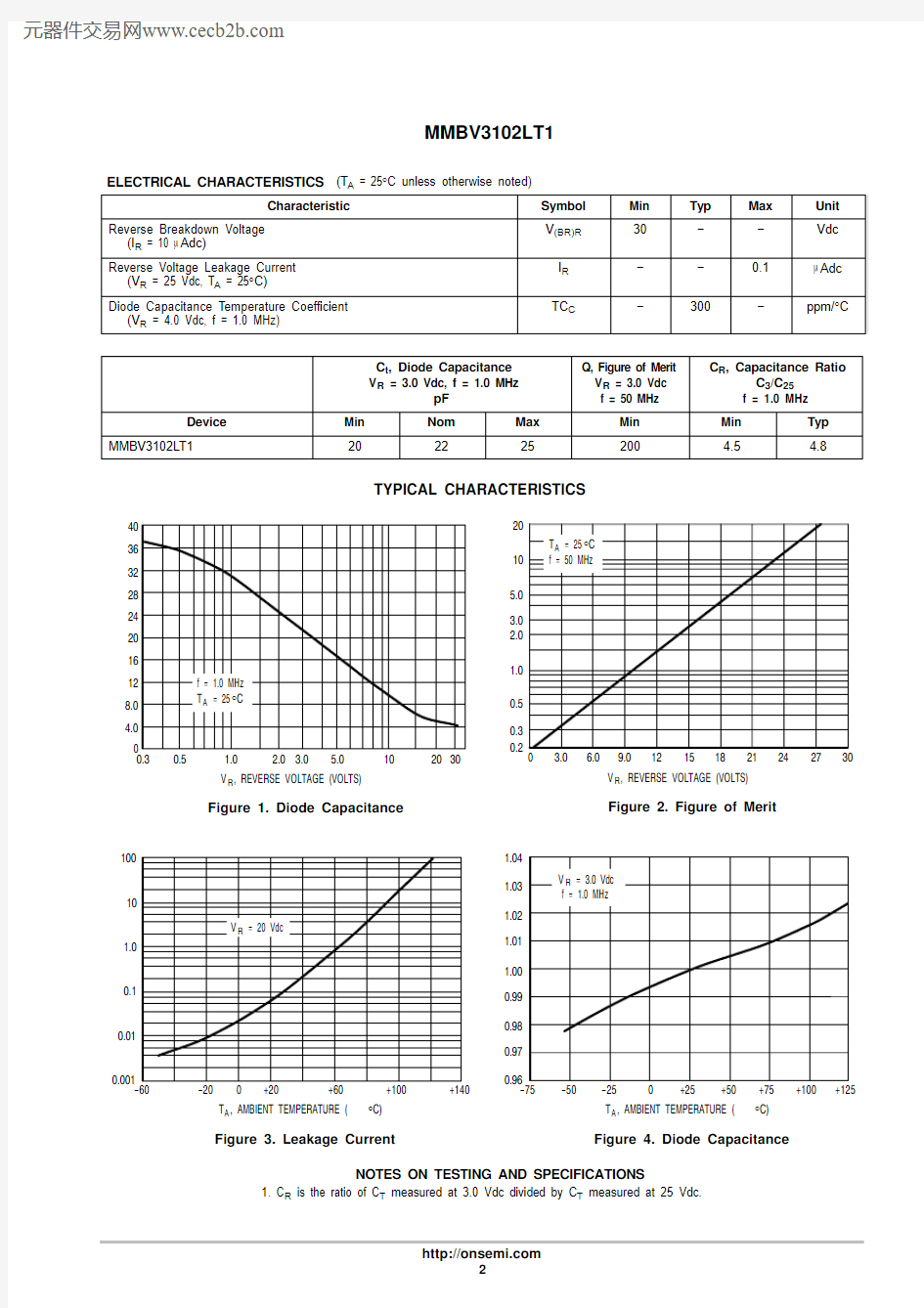
ELECTRICAL CHARACTERISTICS (T A = 25°C unless otherwise noted)
Characteristic
Symbol Min Typ Max Unit Reverse Breakdown Voltage (I R = 10 m Adc)V (BR)R 30??Vdc Reverse Voltage Leakage Current (V R = 25 Vdc, T A = 25°C)
I R ??0.1m Adc Diode Capacitance Temperature Coefficient (V R = 4.0 Vdc, f = 1.0 MHz)
TC C
?
300
?
ppm/°C
C t , Diode Capacitance V R = 3.0 Vdc, f = 1.0 MHz
pF
Q, Figure of Merit V R = 3.0 Vdc f = 50 MHz
C R , Capacitance Ratio
C 3/C 25f = 1.0 MHz Device
Min Nom Max Min Min Typ MMBV3102LT1
20
22
25
200
4.5
4.8
TYPICAL CHARACTERISTICS
Figure 1. Diode Capacitance
Figure 3. Leakage Current T A , AMBIENT TEMPERATURE (°C)Figure 4. Diode Capacitance
T A , AMBIENT TEMPERATURE (°C)
Q , F I G U R E O F M E R I T (x 1000)
202.010, R E V E R S E C U R R E N T (n A )
1000.01
0.001
C T ,
D I O D
E C A P A C I T A N C E (N O R M A L I Z E D )
1.041.021.000.980.96I R 0.1
1.010
1.031.010.990.97NOTES ON TESTING AND SPECIFICATIONS
1. C R is the ratio of C T measured at 3.0 Vdc divided by C T measured at 25 Vdc.
0.3
1.0
10
2030
V R , REVERSE VOLTAGE (VOLTS)C T , D I O D E C A P A C I T A N C E (p F )
0.5
2.0
3.0
5.0
3.05.01.00.50.30.2
PACKAGE DIMENSIONS
SOT?23 (TO?236)
CASE 318?08
ISSUE AN
*For additional information on our Pb?Free strategy and soldering
details, please download the ON Semiconductor Soldering and
Mounting Techniques Reference Manual, SOLDERRM/D.
ON Semiconductor and are registered trademarks of Semiconductor Components Industries, LLC (SCILLC). SCILLC reserves the right to make changes without further notice to any products herein. SCILLC makes no warranty, representation or guarantee regarding the suitability of its products for any particular purpose, nor does SCILLC assume any liability arising out of the application or use of any product or circuit, and specifically disclaims any and all liability, including without limitation special, consequential or incidental damages.
“Typical” parameters which may be provided in SCILLC data sheets and/or specifications can and do vary in different applications and actual performance may vary over time. All operating parameters, including “Typicals” must be validated for each customer application by customer’s technical experts. SCILLC does not convey any license under its patent rights nor the rights of others. SCILLC products are not designed, intended, or authorized for use as components in systems intended for surgical implant into the body, or other applications intended to support or sustain life, or for any other application in which the failure of the SCILLC product could create a situation where personal injury or death may occur. Should Buyer purchase or use SCILLC products for any such unintended or unauthorized application, Buyer shall indemnify and hold SCILLC and its officers, employees, subsidiaries, affiliates, and distributors harmless against all claims, costs, damages, and expenses, and reasonable attorney fees arising out of, directly or indirectly, any claim of personal injury or death associated with such unintended or unauthorized use, even if such claim alleges that SCILLC was negligent regarding the design or manufacture of the part. SCILLC is an Equal Opportunity/Affirmative Action Employer. This literature is subject to all applicable copyright laws and is not for resale in any manner.
PUBLICATION ORDERING INFORMATION