SN65LVDS049PW中文资料

5,0 mm x 6,4 mm
https://www.360docs.net/doc/5017552690.html,
R OUT1
R OUT2
D IN2
D IN1
EN EN
D OUT1+D OUT1?
D OUT2?D OUT2+R IN2?R IN2+R IN1?R IN1+
R R R R D D D D SN65LVDS049
SLLS575–AUGUST 2003
DUAL LVDS DIFFERENTIAL DRIVERS AND RECEIVERS
The intended application of this device and signaling FEATURES
technique is for point-to-point baseband data trans-?DS90LV049Compatible
mission over controlled impedance media of approxi-?Up to 400Mbps Signaling Rates mately 100-?characteristic impedance.The trans-mission media may be printed-circuit board traces,?Flow-Through Pin-out
backplanes,or cables.(Note:The ultimate rate and ?50ps Driver Channel-to-Channel Skew (Typ)distance of data transfer is dependent upon the attenu-?50ps Receiver Channel-to-Channel Skew ation characteristics of the media,the noise coupling to the environment,and other application specific charac-(Typ)
teristics)
? 3.3-V Power Supply
The SN65LVDS049is characterized for operation from ?High-Impedance Disable for all Outputs –40°C to 85°C
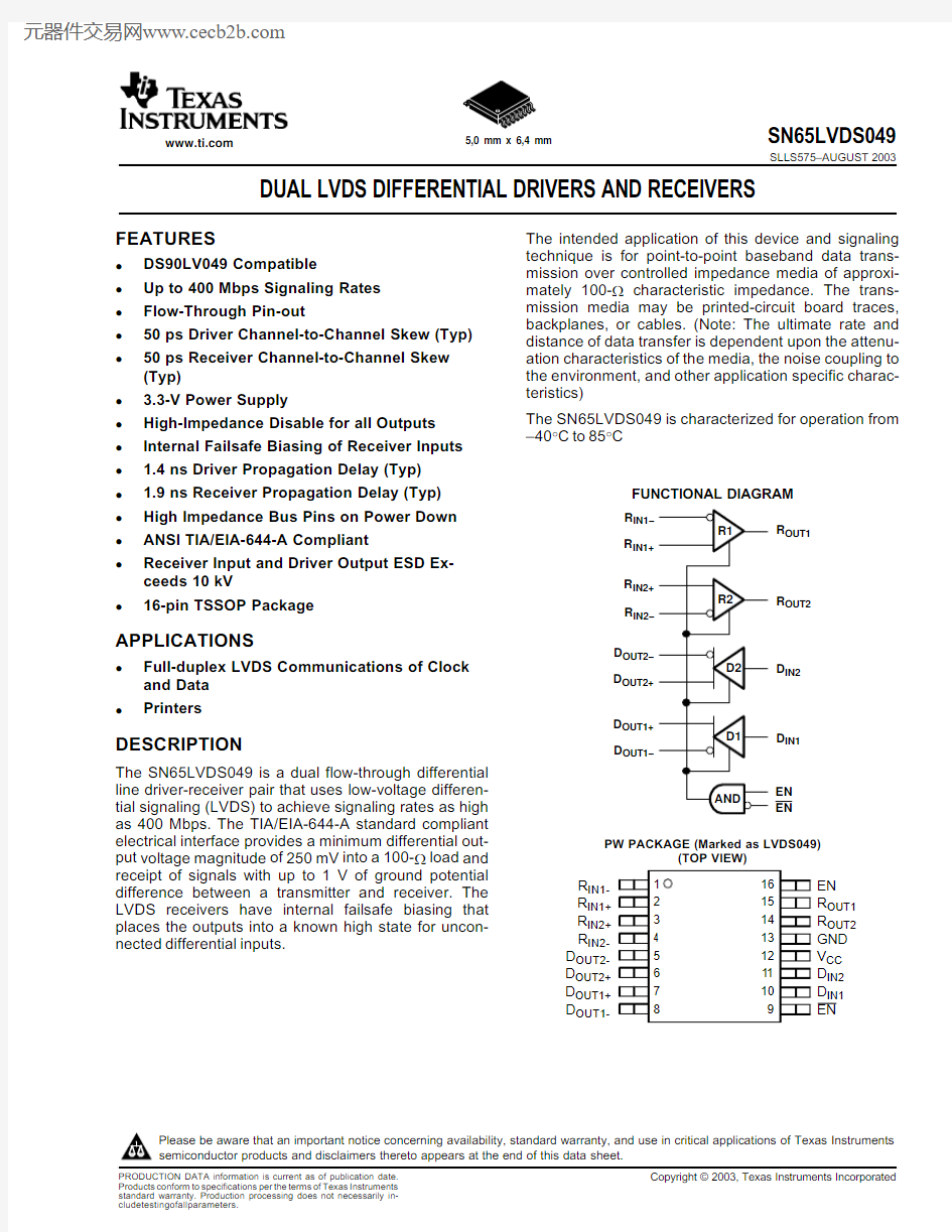
?Internal Failsafe Biasing of Receiver Inputs ? 1.4ns Driver Propagation Delay (Typ)? 1.9ns Receiver Propagation Delay (Typ)FUNCTIONAL DIAGRAM
?High Impedance Bus Pins on Power Down ?ANSI TIA/EIA-644-A Compliant
?Receiver Input and Driver Output ESD Ex-ceeds 10kV
?
16-pin TSSOP Package
APPLICATIONS
?Full-duplex LVDS Communications of Clock and Data ?
Printers
DESCRIPTION
The SN65LVDS049is a dual flow-through differential line driver-receiver pair that uses low-voltage differen-tial signaling (LVDS)to achieve signaling rates as high as 400Mbps.The TIA/EIA-644-A standard compliant electrical interface provides a minimum differential out-PW PACKAGE (Marked as LVDS049)
(TOP VIEW)
put voltage magnitude of 250mV into a 100-?load and receipt of signals with up to 1V of ground potential difference between a transmitter and receiver.The LVDS receivers have internal failsafe biasing that places the outputs into a known high state for uncon-nected differential inputs.
Please be aware that an important notice concerning availability,standard warranty,and use in critical applications of Texas Instruments semiconductor products and disclaimers thereto appears at the end of this data sheet.
PRODUCTION DATA information is current as of publication date.Copyright ?2003,Texas Instruments Incorporated
Products conform to specifications per the terms of Texas Instruments standard warranty.Production processing does not necessarily in-cludetestingofallparameters.
https://www.360docs.net/doc/5017552690.html,
SN65LVDS049
SLLS575–AUGUST 2003
DRIVER TRUTH TABLE
INPUT ENABLES
OUTPUTS (1)
DIN EN EN D OUT+D OUT-L H
L or OPEN
L H H H L X
All other conditions Z
Z
(1)
H =high level,L =low level,X =irrelevant,Z =high impedance (off)
RECEIVER TRUTH TABLE
DIFFERENTIAL INPUT
ENABLES
OUTPUT (1)
R IN--R IN+EN EN R OUT V ID ≥100mV H
L or OPEN
H V ID ≤-100mV L Open/short or terminated
H X
All other conditions Z
(1)
H =high level,L =low level,X =irrelevant,Z =high impedance (off)
ENABLE FUNCTION TABLE
ENABLES
OUTPUTS
EN EN LVDS Out LVCMOS Out L or Open
L or Open DISABLED DISABLED H L or Open
ENABLED ENABLED L or Open
H DISABLED DISABLED H
H
DISABLED
DISABLED
POWER DISSIPATION RATING
CIRCUIT BOARD
T A ≤25°C DERATING FACTOR (1)T A =85°C PACKAGE
MODEL
POWER RATING
ABOVE T A =25°C
POWER RATING
PW
Low-K (2)
774mW
6.2mW/°C
402mW
(1)This is the inverse of the junction-to-ambient thermal resistance when board-mounted and with no air flow.(2)
In accordance with the Low-K thermal metric definitions of EIA/JESD51-3.
2
https://www.360docs.net/doc/5017552690.html,
SN65LVDS049
SLLS575–AUGUST 2003
ABSOLUTE MAXIMUM RATINGS
over operating free-air temperature range (unless otherwise noted)(1)
UNIT
Supply voltage range (2),V CC
-0.3V to 4V D IN ,R OUT ,EN,or EN
-0.3V to (V CC +0.3V)
Voltage range
R IN+or R IN--0.3V to 4V D OUT+or D OUT--0.3V to 3.9V
R IN+,R IN-,D OUT+,and D OUT-±10kV Human Body Model (3)ESD
All pins ±2K V Charged-Device Model (4)
All pins
±500V LVDS output short circuit duration (DOUT+,DOUT-)Continuous
Continuous power dissipation See Dissipation Rating Table
Storage temperature range
-65°C to 150°C
Lead temperature 1,6mm (1/16inch)from case for 10seconds 260°C
(1)
Stresses beyond those listed under "absolute maximum ratings"may cause permanent damage to the device.These are stress ratings only and functional operation of the device at these or any other conditions beyond those indicated under "recommended operating conditions"is not implied.Exposure to absolute-maximum-rated conditions for extended periods may affect device reliability (2)All voltage values,except differential I/O bus voltages,are with respect to network ground terminal.(3)Tested in accordance with JEDEC Standard 22,Test Method A114-A.(4)
Tested in accordance with JEDEC Standard 22,Test Method C101.
RECOMMENDED OPERATING CONDITIONS
3
https://www.360docs.net/doc/5017552690.html,
SN65LVDS049
SLLS575–AUGUST 2003
DEVICE ELECTRICAL CHARACTERISTICS
over recommended operating conditions (unless otherwise noted)
PARAMETER
TEST CONDITIONS
MIN
TYP (1)
MAX
UNIT
INPUT DC SPECIFICATIONS (D IN ,EN,EN)V IH Input high voltage 2.0V CC V V IL Input low voltage GND 0.8V I IH Input high current V IN =V CC -10310μA I IL Input low current V IN =GND -10110
μA V CL Input clamp voltage I CL =-18mA
-1.5-0.8V LVDS Output DC Specifications (D OUT+,D OUT-)
|V OD |Differential output voltage 250350450V Change in magnitude of V OD for ?|V OD |-35
135mV complimentary output states R L =100?,See Figure 1
V OS Offset voltage
1.125 1.2 1.375V Change in magnitude of V OS for ?V OS -25
125mV complimentary output states Enabled
I OS Output short circuit current
D IN =V CC and D OUT+=0V,or -4.5-9mA D IN =GND and D OUT-=0V I OSD Differential output short circuit current (2)Enabled,V OD =0V -3.6-9mA I OFF Power-off leakage
V CC =0V or Open;-20020μA VO =0or 3.6V I OZ
Output high-impedance current
EN =0V and EN =V CC ,-10
10μA
V O =0or V CC
LVDS Input DC Specifications (R IN+,R IN-)V IT+Differential input high threshold 100
mV V CM =1.2V,0.05V,2.35V V IT-Differential input low threshold -100mV V CMR Common-mode voltage range V ID =±100mV
0.05 2.35V V CC =3.6V,V IN =0V or 2.8V -2020μA I IN
Input current
V CC =0V,V IN =0V,2.8V,or 3.6V -2020
μA Outputs DC Specifications (R OUT )V OH Output high voltage I OH =-0.4mA,V ID =200mV 2.7
3.3V V OL Output Low voltage
I OL =2mA,V ID =-200mV 0.050.25V I OZ Output high-impedance current Disabled,V OUT =0V or V CC
-10
010μA Device DC Specifications
I CC Power supply current EN =3.3V,D IN =V CC or Gnd,100-?1735mA (LVDS loaded,enabled)
differential LVDS loads I CCZ High impedance supply current (disabled)
No loads,EN =0V
1
25mA
(1)All typical values are at 25°C and with a 3.3V supply.
(2)
Output short circuit current (IOS)is specified as magnitude only,the minus sign indicates direction only
4
https://www.360docs.net/doc/5017552690.html, SN65LVDS049 SLLS575–AUGUST2003
SWITCHING CHARACTERISTICS
over operating free-air temperature range(unless otherwise noted)
PARAMETER TEST CONDITIONS MIN TYP(1)MAX UNIT LVDS Outputs(D OUT+,D OUT-)
t PLHD Differential propagation delay low to high R L=100?, 1.3 2.0ns
C L=15pF distributed,
t PHLD Differential propagation delay high to low 1.4 2.0ns
See Figure2
t sk(p)Differential pulse skew(|t PHL-t PLH|)00.150.4ns t sk(o)Differential channel-to-channel skew(2)00.050.5ns t sk(pp)Differential part-to-part skew(3)01ns t r Differential rise time0.20.51ns t f Differential fall time0.20.51ns t PHZ Disable time,high level to high impedance R L=100?, 2.74ns
C L=15pF distributed,
t PLZ Disable time,low level to high impedance 2.74ns
See Figure3
t PZH Enable time,high impedance to high level158ns t PZL Enable time,high impedance to low level158ns f MAX Maximum operating frequency(4)250MHz LVCMOS Outputs(R OUT)
t PLH Propagation delay low to high V ID=200mV,0.5 1.9 3.5ns
C L=15pF distributed,
t PHL Propagation delay high to low0.5 1.7 3.5ns
See Figure4
t sk(p)Pulse skew(|t PHL-t PLH|)00.20.4ns t sk(o)Channel-to-channel skew(5)00.050.5ns t sk(pp)Part-to-part skew(6)01ns t r Rise time0.30.5 1.4ns t f Fall time0.30.5 1.4ns t PHZ Disable time,high level to high impedance C L=15pF distributed,37.29ns
See Figure5
t PLZ Disable time,low level to high impedance 2.548ns t PZH Enable time,high impedance to high level 2.5 4.27ns t PZL Enable time,high impedance to low level2 3.37ns
f MAX Maximum operatin
g frequency(7)200250MHz
(1)All typical values are at25°C and with a3.3V supply.
(2)t
sk(o)is the magnitude of the time difference between the t PLH or t PHL of all drivers of a single device with all of their inputs connected
together.
(3)t
sk(pp)is the magnitude of the difference in propagation delay times between any specified terminals of two devices when both devices
operate with the same supply voltages,at the same temperature,and have identical packages and test circuits.
(4)f
(MAX)generator input conditions:t r=t f<1ns(0%to100%),50%duty cycle,0V to3V.Output Criteria:duty cycle=45%to55%,V OD
>250mV,all channels switching.
(5)t
sk(lim)is the maximum delay time difference between drivers over temperature,V CC,and process.
(6)tsk(pp)is the magnitude of the difference in propagation delay times between any specified terminals of two devices when both
devices operate wf(MAX)generaith the same supply voltages,at the same temperature,and have identical packages and test circuits
(7)f
(MAX)generator input conditions:t r=t f<1ns(0%to100%),50%duty cycle,V ID=200mV,V CM=1.2V.Output criteria:duty cycle=
45%to55%,V OH>2.7V,V OL<0.25V,all channels switching.
5
https://www.360docs.net/doc/5017552690.html,
V CC GND
OD
SN65LVDS049
SLLS575–AUGUST 2003
EQUIVALENT INPUT AND OUTPUT SCHEMATIC DIAGRAMS
PARAMETER MEASUREMENT INFORMATION
Figure 1.Driver V OD and V OS Test Circuit
6
https://www.360docs.net/doc/5017552690.html,
Oscilloscope
3 V 0 V
V OH V OL
D D OUT-D V
V OH
V OL
0 V 3 V
0 V 3 V
1.2 V
1.2 V t t EN When EN = GND or Open
D OUT+ When D IN = GND D OUT- When D IN = V CC
EN When EN = V CC
D OUT- When D IN = GND D OUT+ When D IN = V CC SN65LVDS049
SLLS575–AUGUST 2003
Figure 2.Driver Propagation Delay and Rise/Fall Time Test Circuit and Waveforms
Figure 3.Driver High-Impedance State Delay Test Circuit and Waveforms
7
https://www.360docs.net/doc/5017552690.html,
1.3 V
1.1 V
V OH
V OL
R IN-R IN+
R OUT
V OH
V OL
0 V
3 V
V CC /2V CC /2
0 V 3 V
t t EN When EN = GND or OPEN
EN When EN = V CC
R OUT for R IN+ = 1.4 V
and R IN- = 1 V
R OUT for R IN+ = 1 V and R IN- = 1.4 V
SN65LVDS049
SLLS575–AUGUST 2003
Figure 4.Receiver Propagation Delay and Rise/Fall Test Circuit and Waveforms
Figure 5.Receiver High-Impedance State Delay Test Circuit and Waveforms
(Note,V CC =3.3V)
8
https://www.360docs.net/doc/5017552690.html,
100
200
300
400500
60040
60
80100120140
160
|V O D - D i f f e r e n t i a l O u t p u t V o l t a g e - m V
|R L - Load Resistance - ?
010
20
30
40
50
60
0.1
1
10100
1000
I C C - S u p p l y C u r r e n t - m A
f - Frequency - MHz
SN65LVDS049
SLLS575–AUGUST 2003
TYPICAL CHARACTERISTICS
Power Supply Current
V vs.Load Resistance
vs.Frequency
Figure 6.
Figure 7.
9
元器件交易网https://www.360docs.net/doc/5017552690.html,
IMPORTANT NOTICE
Texas Instruments Incorporated and its subsidiaries (TI) reserve the right to make corrections, modifications,
enhancements, improvements, and other changes to its products and services at any time and to discontinue
any product or service without notice. Customers should obtain the latest relevant information before placing
orders and should verify that such information is current and complete. All products are sold subject to TI’s terms
and conditions of sale supplied at the time of order acknowledgment.
TI warrants performance of its hardware products to the specifications applicable at the time of sale in
accordance with TI’s standard warranty. Testing and other quality control techniques are used to the extent TI
deems necessary to support this warranty. Except where mandated by government requirements, testing of all
parameters of each product is not necessarily performed.
TI assumes no liability for applications assistance or customer product design. Customers are responsible for
their products and applications using TI components. To minimize the risks associated with customer products
and applications, customers should provide adequate design and operating safeguards.
TI does not warrant or represent that any license, either express or implied, is granted under any TI patent right,
copyright, mask work right, or other TI intellectual property right relating to any combination, machine, or process
in which TI products or services are used. Information published by TI regarding third-party products or services
does not constitute a license from TI to use such products or services or a warranty or endorsement thereof.
Use of such information may require a license from a third party under the patents or other intellectual property
of the third party, or a license from TI under the patents or other intellectual property of TI.
Reproduction of information in TI data books or data sheets is permissible only if reproduction is without
alteration and is accompanied by all associated warranties, conditions, limitations, and notices. Reproduction
of this information with alteration is an unfair and deceptive business practice. TI is not responsible or liable for
such altered documentation.
Resale of TI products or services with statements different from or beyond the parameters stated by TI for that
product or service voids all express and any implied warranties for the associated TI product or service and
is an unfair and deceptive business practice. TI is not responsible or liable for any such statements.
Following are URLs where you can obtain information on other Texas Instruments products and application
solutions:
Products Applications
Amplifiers https://www.360docs.net/doc/5017552690.html, Audio https://www.360docs.net/doc/5017552690.html,/audio
Data Converters https://www.360docs.net/doc/5017552690.html, Automotive https://www.360docs.net/doc/5017552690.html,/automotive
DSP https://www.360docs.net/doc/5017552690.html, Broadband https://www.360docs.net/doc/5017552690.html,/broadband
Interface https://www.360docs.net/doc/5017552690.html, Digital Control https://www.360docs.net/doc/5017552690.html,/digitalcontrol
Logic https://www.360docs.net/doc/5017552690.html, Military https://www.360docs.net/doc/5017552690.html,/military
Power Mgmt https://www.360docs.net/doc/5017552690.html, Optical Networking https://www.360docs.net/doc/5017552690.html,/opticalnetwork
Microcontrollers https://www.360docs.net/doc/5017552690.html, Security https://www.360docs.net/doc/5017552690.html,/security
Telephony https://www.360docs.net/doc/5017552690.html,/telephony
Video & Imaging https://www.360docs.net/doc/5017552690.html,/video
Wireless https://www.360docs.net/doc/5017552690.html,/wireless
Mailing Address:Texas Instruments
Post Office Box 655303 Dallas, Texas 75265
Copyright 2003, Texas Instruments Incorporated