MM74C04M中文资料

October 1987Revised January 1999
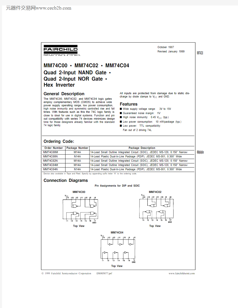
MM74C00 ? MM74C02 ? MM74C04 Quad 2-Input NAND Gate ? Quad 2-Input NOR Gate ? Hex Inverter
? 1999 Fairchild Semiconductor Corporation
DS005877.prf
https://www.360docs.net/doc/682427684.html,
MM74C00 ? MM74C02 ? MM74C04Quad 2-Input NAND Gate ? Quad 2-Input NOR Gate ? Hex Inverter
General Description
The MM74C00, MM74C02, and MM74C04 logic gates employ complementary MOS (CMOS) to achieve wide power supply operating range, low power consumption,high noise immunity and symmetric controlled rise and fall times. With features such as this the 74C logic family is close to ideal for use in digital systems. Function and pin out compatibility with series 74 devices minimizes design time for those designers already familiar with the standard 74 logic family.All inputs are protected from damage due to static dis-charge by diode clamps to V CC and GND.
Features
s Wide supply voltage range: 3V to 15V s Guaranteed noise margin:1V
s High noise immunity:0.45 V CC (typ.)
s Low power consumption:10 nW/package (typ.)
s Low power:TTL compatibility:
Fan out of 2 driving 74L
Ordering Code:
Device also available in Tape and Reel. Specify by appending suffix letter “X” to the ordering code.
Connection Diagrams
Pin Assignments for DIP and SOIC
MM74C00
Top View
MM74C02
Top View
MM74C04
Top View
Order Number Package Number
Package Description
MM74C00M M14A 14-Lead Small Outline Integrated Circuit (SOIC), JEDEC MS-120, 0.150” Narrow MM74C00N N14A 14-Lead Plastic Dual-In-Line Package (PDIP), JEDEC MS-001, 0.300” Wide MM74C02N M14A 14-Lead Small Outline Integrated Circuit (SOIC), JEDEC MS-120, 0.150” Narrow MM74C04M M14A 14-Lead Small Outline Integrated Circuit (SOIC), JEDEC MS-120, 0.150” Narrow MM74C04N
N14A
14-Lead Plastic Dual-In-Line Package (PDIP), JEDEC MS-001, 0.300” Wide
https://www.360docs.net/doc/682427684.html, 2
M M 74C 00 ? M M 74C 02 ? M M 74C 04
Absolute Maximum Ratings (Note 1)
Note 1: “Absolute Maximum Ratings” are those values beyond which the safety of the device cannot be guaranteed. Except for “Operating Tempera-ture Range” they are not meant to imply that the devices should be oper-ated at these limits. The table of “Electrical Characteristics” provides conditions for actual device operation.
DC Electrical Characteristics
Min/Max limits apply across the guaranteed temperature range unless otherwise noted AC Electrical Characteristics (Note 2)
T A = 25°C, C L = 50 pF , unless otherwise specified Note 2: AC Parameters are guaranteed by DC correlated testing.Note 3: Capacitance is guaranteed by periodic testing.
Note 4: C PD determines the no load AC power consumption of any CMOS device. For complete explanation see Family Characteristics Application Note—AN-90.
Voltage at Any Pin
?0.3V to V CC + 0.3V
Operating T emperature Range ?40°C to +85°C Storage T emperature Range ?65°C to +150°C
Operating V CC Range 3.0V to 15V
Maximum V CC Voltage 18V
Power Dissipation (P D )Dual-In-Line 700 mW Small Outline
500 mW
Lead Temperature (Soldering, 10 seconds)
300°C
Symbol Parameter
Conditions
Min
Typ
Max
Units
CMOS TO CMOS V IN(1)Logical “1” Input Voltage V CC = 5.0V 3.5V V CC = 10V 8.0
V V IN(0)Logical “0” Input Voltage V CC = 5.0V 1.5V V CC = 10V
2.0
V V OUT(1)Logical “1” Output Voltage V CC = 5.0V , I O = ?10 μA 4.5V V CC = 10V , I O = ?10 μA 9.0
V V OUT(0)Logical “0” Output Voltage V CC = 5.0V , I O = 10 μA 0.5V V CC = 10V , I O = 10 μA 1.0V I IN(1)Logical “1” Input Current V CC = 15V , V IN = 15V 0.005 1.0
μA I IN(0)Logical “0” Input Current V CC = 15V , V IN = 0V ?1.0
?0.005μA I CC Supply Current
V CC = 15V 0.01
15
μA LOW POWER TO CMOS
V IN(1)Logical “1” Input Voltage 74C, V CC = 4.75V V CC ? 1.5
V V IN(0)Logical “0” Input Voltage 74C, V CC = 4.75V
0.8
V V OUT(1)Logical “1” Output Voltage 74C, V CC = 4.75V , I O = ?10 μA 4.4
V V OUT(0)Logical “0” Output Voltage 74C, V CC = 4.75V , I O = 10 μA 0.4
V CMOS TO LOW POWER
V IN(1)Logical “1” Input Voltage 74C, V CC = 4.75V 4.0
V V IN(0)Logical “0” Input Voltage 74C, V CC = 4.75V
1.0
V V OUT(1)Logical “1” Output Voltage 74C, V CC = 4.75V , I O = ?360 μA 2.4
V V OUT(0)
Logical “0” Output Voltage
74C, V CC = 4.75V , I O = 360 μA
0.4
V
OUTPUT DRIVE (see Family Characteristics Data Sheet) T A = 25°C (short circuit current)I SOURCE Output Source Current V CC = 5.0V , V IN(0) = 0V , V OUT = 0V ?1.75mA I SOURCE Output Source Current V CC = 10V , V IN(0) = 0V , V OUT = 0V ?8.0mA I SINK Output Sink Current V CC = 5.0V , V IN(1) = 5.0V , V OUT = V CC 1.75mA I SINK
Output Sink Current
V CC = 10V , V IN(1) = 10V, V OUT = V CC
8.0
mA
Symbol
Parameter
Conditions
Min
Typ
Max
Units
MM74C00, MM74C02, MM74C04t pd0, t pd1Propagation Delay Time to V CC = 5.0V 5090ns Logical “1” or “0”V CC = 10V 3060
ns C IN Input Capacitance
(Note 3)
6.0pF C PD
Power Dissipation Capacitance
Per Gate or Inverter (Note 4)
12
pF
https://www.360docs.net/doc/682427684.html, MM74C00 ? MM74C02 ? MM74C04
Typical Performance Characteristics
Gate Transfer Characteristics
Guaranteed Noise Margin
Over Temperature vs V CC
Power Dissipation vs Frequency
MM74C00, MM74C02, MM74C04
Propagation Delay vs
Ambient Temperature
MM74C00, MM74C02, MM74C04
Propagation Delay vs
Ambient Temperature
MM74C00, MM74C02, MM74C04
Propagation Delay Time vs
Load Capacitance
MM74C00, MM74C02, MM74C04
https://www.360docs.net/doc/682427684.html, 4
M M 74C 00 ? M M 74C 02 ? M M 74C 04
Switching Time Waveforms and AC Test Circuit
CMOS to CMOS
Delays measured with input t r , t f ≤ 20 ns.
https://www.360docs.net/doc/682427684.html,
MM74C00 ? MM74C02 ? MM74C04
Physical Dimensions inches (millimeters) unless otherwise noted
14-Lead Small Outline Integrated Circuit (SOIC), JEDEC MS-120, 0.150” Narrow
Package Number M14A
F a irch ild d o e s n o t a ssu m e a n y re spo n sib ility fo r u se o f a n y circu itry de scrib e d , n o circu it pa ten t lice nse s a re im p lie d a nd F a irch ild re se rv e s the rig h t a t a n y tim e w ith ou t n o tice to cha n g e sa id circu itry an d sp e cifica tio n s.
M M 74C 00 ? M M 74C 02 ? M M 74C 04 Q u a d 2-I n p u t N A N D G a t e ? Q u a d 2-I n p u t N O R G a t e ? H e x I n v e r t e r
LIFE SUPPORT POLICY
FAIRCHILD’S PRODUCTS ARE NOT AUTHORIZED FOR USE AS CRITICAL COMPONENTS IN LIFE SUPPORT
DEVICES OR SYSTEMS WITHOUT THE EXPRESS WRITTEN APPROVAL OF THE PRESIDENT OF FAIRCHILD SEMICONDUCTOR CORPORATION. As used herein:
1.Life support devices or systems are devices or systems
which, (a) are intended for surgical implant into the
body, or (b) support or sustain life, and (c) whose failure
to perform when properly used in accordance with
instructions for use provided in the labeling, can be rea-sonably expected to result in a significant injury to the user.
2. A critical component in any component of a life support device or system whose failure to perform can be rea-sonably expected to cause the failure of the life support device or system, or to affect its safety or https://www.360docs.net/doc/682427684.html, Physical Dimensions inches (millimeters) unless otherwise noted (Continued)
14-Lead Plastic Dual-In-Line Package (PDIP), JEDEC MS-001, 0.300” Wide
Package Number N14A