Dual-Band Superconducting Bandpass Filter Using Quadruple-Mode Resonator v13(Final version)
Technical Notes
Dual-Band Superconducting Bandpass Filter
Using Quadruple-Mode Resonator
Haiwen Liu,Member,IEEE,Pin Wen,Yulong Zhao,Baoping Ren, Xiaomei Wang,and Xuehui Guan,Member,IEEE Abstract—A dual-band high-temperature superconducting(HTS)band-pass?lter(BPF)using a quadruple-mode resonator is realized in this paper.The resonator consists of a half-wavelength uniform impedance resonator,an open stub in a symmetrical plane,and two spiral open stubs at the two sides of the symmetrical plane.Distinct characteristics of the quadruple-mode resonator are investigated by using even/odd mode theory,and the design graphs are given to analyze the dual-band?lter.A dual-band HTS BPF with central frequencies of1.8GHz for GSM applica-tions and2.4GHz for wireless local area network applications is designed using the proposed quadruple-mode resonator,which is fabricated by depositing YBCO?lms on a0.5-mm-thick MgO substrate.Its size occupies only13mm×17mm.Measured results demonstrate that an insertion loss within the passbands is less than0.25dB.In addition,a transmission zero is achieved in-between two passbands,and two transmission zeros are realized in the upper stopband of the higher passband,which improve the skirt selectivity and stopband characteristics of the?lter.
Index Terms—Bandpass?lter(BPF),dual band,even and odd modes, quad-mode resonator,superconductor.
I.I NTRODUCTION
I N MODERN wireless and mobile communication systems,multi-
band radio-frequency/microwave?lters are important and essential components.As a result,dual-band bandpass?lters(BPFs)are exten-sively investigated,and various design approaches have been proposed [1]–[3].However,some attempts have so far been made in dual-band BPFs constructed using high temperature superconductors(HTSs) [4]–[8].
It is well known that a microwave HTS device has lower loss and better performance than a normal conducting one.Two popular methods for designing dual-band BPFs are currently available.The ?rst method mainly involves constructing a coupling matrix with a multiband response using direct optimization[4].The second method involves using dual-frequency resonators,such as stepped-impedance resonators[5],embedded resonators[6],and stub-loaded resonators
[7],[8].
A dual-band HTS BPF with high isolation between two frequency bands that are only a few tens of megahertz apart is realized in[9]. Furthermore,transmission zeros(TZs)are placed in between the two frequency bands using electromagnetic coupling between nonadjacent resonators,which results in high isolation between the two bands. Another dual-band superconducting BPF using an embedded split-ring resonator for wireless local area network(WLAN)and Worldwide Interoperability for Microwave Access(WiMAX)applications is pro-
Manuscript received July26,2013;revised October11,2013and December 1,2013;accepted December8,2013.Date of publication December11,2013; date of current version January25,2014.This work was supported in part by the National Science Foundation of China under Grant61061001and in part by the 555Talent Program of Jiangxi Province of China.This paper was recommended by Associate Editor D.E.Oates.
The authors are with East China Jiaotong University,Nanchang330013, China(e-mail:liuhaiwen@https://www.360docs.net/doc/629112678.html,).
Color versions of one or more of the?gures in this paper are available online at https://www.360docs.net/doc/629112678.html,.
Digital Object Identi?er
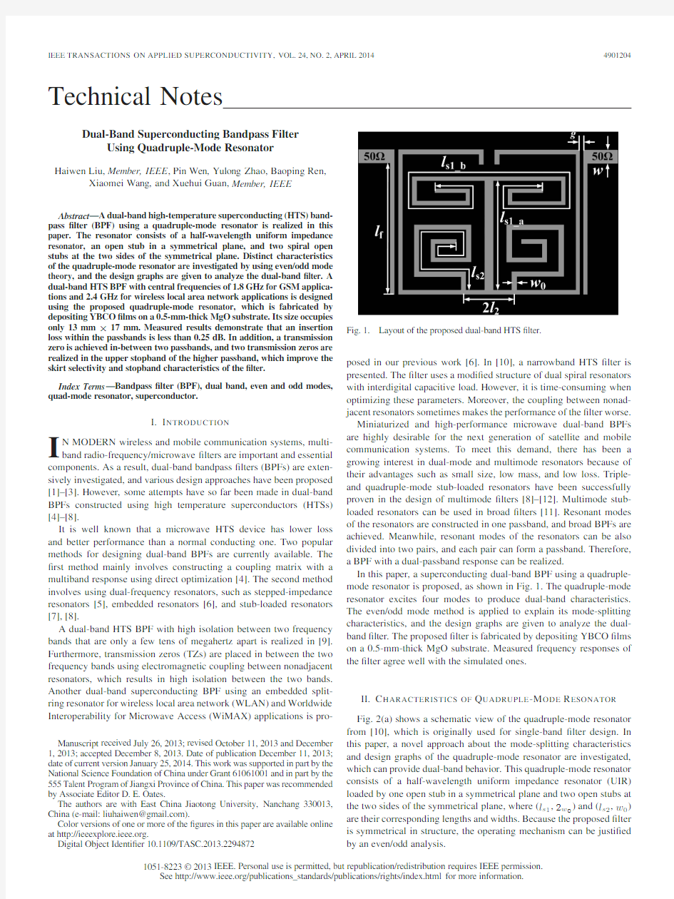
10.1109/https://www.360docs.net/doc/629112678.html,yout of the proposed dual-band HTS?lter.
posed in our previous work[6].In[10],a narrowband HTS?lter is presented.The?lter uses a modi?ed structure of dual spiral resonators with interdigital capacitive load.However,it is time-consuming when optimizing these parameters.Moreover,the coupling between nonad-jacent resonators sometimes makes the performance of the?lter worse. Miniaturized and high-performance microwave dual-band BPFs are highly desirable for the next generation of satellite and mobile communication systems.To meet this demand,there has been a growing interest in dual-mode and multimode resonators because of their advantages such as small size,low mass,and low loss.Triple-and quadruple-mode stub-loaded resonators have been successfully proven in the design of multimode?lters[8]–[12].Multimode stub-loaded resonators can be used in broad?lters[11].Resonant modes of the resonators are constructed in one passband,and broad BPFs are achieved.Meanwhile,resonant modes of the resonators can be also divided into two pairs,and each pair can form a passband.Therefore, a BPF with a dual-passband response can be realized.
In this paper,a superconducting dual-band BPF using a quadruple-mode resonator is proposed,as shown in Fig.1.The quadruple-mode resonator excites four modes to produce dual-band characteristics. The even/odd mode method is applied to explain its mode-splitting characteristics,and the design graphs are given to analyze the dual-band?lter.The proposed?lter is fabricated by depositing YBCO?lms on a0.5-mm-thick MgO substrate.Measured frequency responses of the?lter agree well with the simulated ones.
II.C HARACTERISTICS OF Q UADRUPLE-M ODE R ESONATOR Fig.2(a)shows a schematic view of the quadruple-mode resonator from[10],which is originally used for single-band?lter design.In this paper,a novel approach about the mode-splitting characteristics and design graphs of the quadruple-mode resonator are investigated, which can provide dual-band behavior.This quadruple-mode resonator consists of a half-wavelength uniform impedance resonator(UIR) loaded by one open stub in a symmetrical plane and two open stubs at the two sides of the symmetrical plane,where(l s1,2w
)and(l s2,w0) are their corresponding lengths and widths.Because the proposed?lter is symmetrical in structure,the operating mechanism can be justi?ed by an even/odd analysis.
1051-8223?2013IEEE.Personal use is permitted,but republication/redistribution requires IEEE permission.
See https://www.360docs.net/doc/629112678.html,/publications_standards/publications/rights/index.html for more information.
Fig.2.(a)Schematic view of the quadruple-mode resonator.(b)Even-mode equivalent circuit.(c)Odd-mode equivalent circuit.
The symmetrical plane(T?T )in Fig.2will behave as an electric wall or a magnetic wall under the odd-mode or even-mode excitation, respectively.Y in?odd and Y in?even represent the input admittances of the odd-mode and the even-mode equivalent circuits,respectively. Following the transmission line theory,Y in?odd and Y in?even can be derived as
Y in?odd=jY0
tanθ1+tanθs2?cotθ2
1?tanθ1(tanθs2?cotθ2)
(1)
Y in?even=jY0
tanθ1+tanθs2+tan(θs1+θ2)
1?tanθ1[tanθs2+tan(θs1+θ2)]
(2)
whereθ1=βl1,θ2=βl2,θs1=βl s1,θs2=βl s2,andβis the propagation constant.Y0denotes the characteristic admittance respect to the width w0of the transmission line.
Under the odd-mode excitation,the resonance condition can be derived by setting Y in?odd=0.Two odd-mode frequencies,i.e.,f o1 and f o2,can be excited and deduced as follows:
tanθ1+tanθs2?cotθ2=0.(3)
Similarly,under the even-mode excitation,two even-mode frequen-cies,i.e.,f e1and f e2,can be produced by setting Y in?even=0.They are derived as follows:
tanθ1+tanθs2+tan(θs1+θ2)=0.(4)
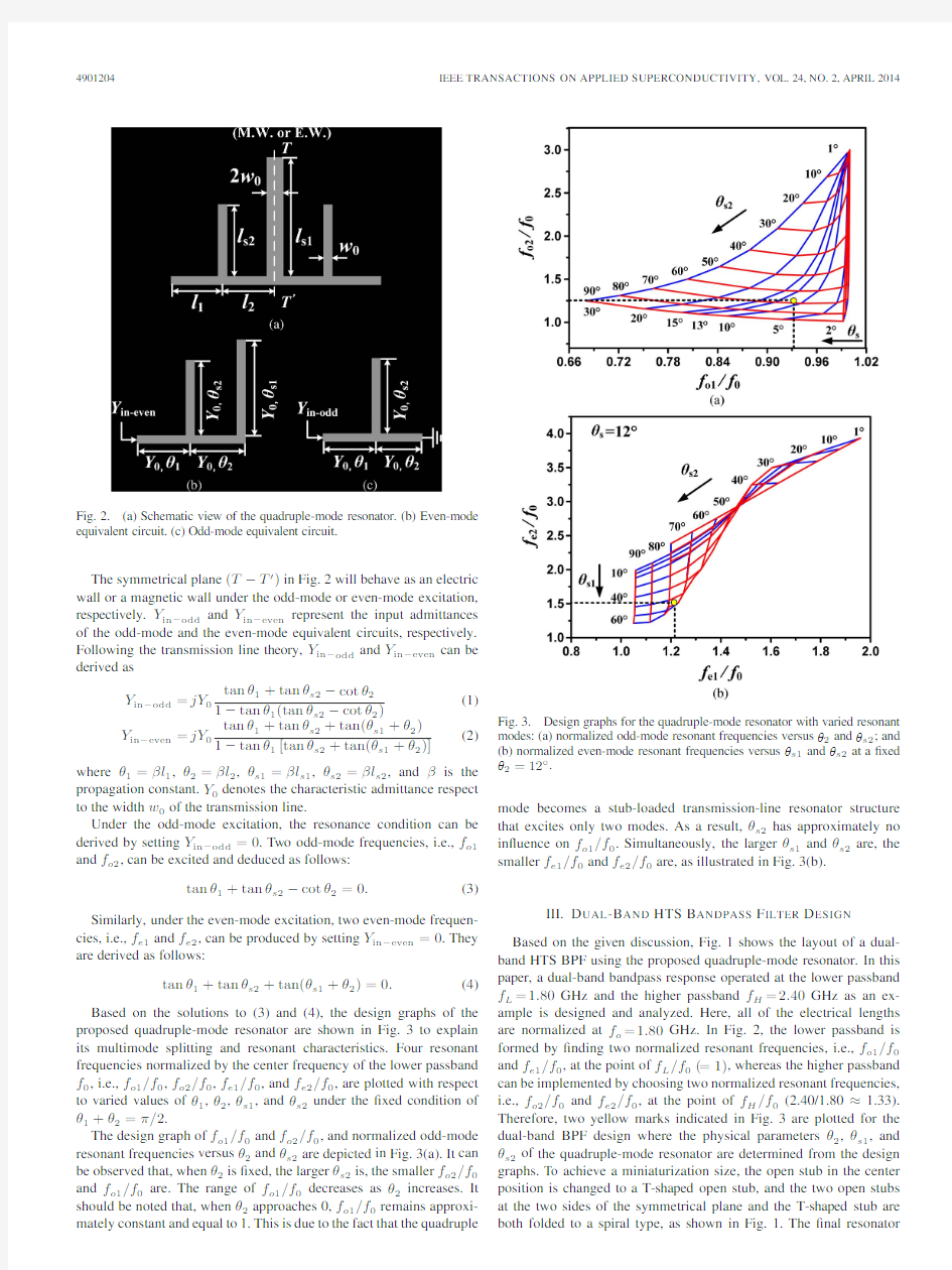
Based on the solutions to(3)and(4),the design graphs of the proposed quadruple-mode resonator are shown in Fig.3to explain its multimode splitting and resonant characteristics.Four resonant frequencies normalized by the center frequency of the lower passband f0,i.e.,f o1/f0,f o2/f0,f e1/f0,and f e2/f0,are plotted with respect to varied values ofθ1,θ2,θs1,andθs2under the?xed condition of θ1+θ2=π/2.
The design graph of f o1/f0and f o2/f0,and normalized odd-mode resonant frequencies versusθ2andθs2are depicted in Fig.3(a).It can be observed that,whenθ2is?xed,the largerθs2is,the smaller f o2/f0 and f o1/f0are.The range of f o1/f0decreases asθ2increases.It should be noted that,whenθ2approaches0,f o1/f0remains approxi-mately constant and equal to1.This is due to the fact that the
quadruple Fig.3.Design graphs for the quadruple-mode resonator with varied resonant modes:(a)normalized odd-mode resonant frequencies versusθ2andθs2;and (b)normalized even-mode resonant frequencies versusθs1andθs2at a?xed θ2=12?.
mode becomes a stub-loaded transmission-line resonator structure that excites only two modes.As a result,θs2has approximately no in?uence on f o1/f0.Simultaneously,the largerθs1andθs2are,the smaller f e1/f0and f e2/f0are,as illustrated in Fig.3(b).
III.D UAL-B AND HTS B ANDPASS F ILTER D ESIGN Based on the given discussion,Fig.1shows the layout of a dual-band HTS BPF using the proposed quadruple-mode resonator.In this paper,a dual-band bandpass response operated at the lower passband f L=1.80GHz and the higher passband f H=2.40GHz as an ex-ample is designed and analyzed.Here,all of the electrical lengths are normalized at f o=1.80GHz.In Fig.2,the lower passband is formed by?nding two normalized resonant frequencies,i.e.,f o1/f0 and f e1/f0,at the point of f L/f0(=1),whereas the higher passband can be implemented by choosing two normalized resonant frequencies, i.e.,f o2/f0and f e2/f0,at the point of f H/f0(2.40/1.80≈1.33). Therefore,two yellow marks indicated in Fig.3are plotted for the dual-band BPF design where the physical parametersθ2,θs1,and θs2of the quadruple-mode resonator are determined from the design graphs.To achieve a miniaturization size,the open stub in the center position is changed to a T-shaped open stub,and the two open stubs at the two sides of the symmetrical plane and the T-shaped stub are both folded to a spiral type,as shown in Fig.1.The?nal resonator
Fig.4.Simulated surface current density distributions for the dual-band?lter.
(a)f o1=1.81GHz.(b)f e1=1.84GHz.(c)f o2=2.42GHz.(d)f e2=
2.44GHz.
structure not only has a miniature size but also has the same resonant
characteristics with the basic resonator structure.
Following the earlier discussion,a compact dual-band super-
conducting?lter was designed,simulated,and measured.It is noted
that the proposed quadruple-mode resonator is meandered to realize
compactness of the structure.The dimensions of the?lter,which
is shown in Fig.1,are optimized as follows:l1=14.65mm,l2=
1.15mm,l s1_a=5.4mm,l s1_b=19.3mm,l s2=13.35mm,l f=
6.6mm,w=0.5mm,w0=0.2mm,and g=0.05mm.The whole
?lter circuit size occupies13mm×17mm,which corresponds
to0.20λg×0.26λg,whereλg is the guided wavelength at f L on the MgO substrate.The designed dual-band superconducting BPF
is simulated by a commercial electromagnetic(EM)simulator,i.e.,
Sonnet V11.54[15].
Simulated current density distributions of the quadruple-mode reso-
nant characteristics are depicted in Fig.4.The surface current density
distributions at four resonant frequencies f o1=1.81GHz,f e1=
1.84GHz,f o2=
2.42GHz,and f e2=2.44GHz are displayed in
Fig.4(a)–(d),respectively.As shown in Fig.4(a)and(b),at the?rst
odd resonant mode f o1and at the?rst even resonant mode f e1,the
current travels around the half-wavelength UIR and the open stub in
the symmetrical plane.Thus,two resonant frequencies f o1and f e1
consist of the lower passband.Meanwhile,the higher passband have
two poles at f o2=2.42GHz and f e2=2.44GHz,which are shown
in Fig.4(c)and(d),respectively.At the higher passband,the half-
wavelength resonator and the two spiral open stubs at the two side
of symmetrical have obvious current density distribution.Therefore,
the lower passband frequency f L is mainly both determined by the
half-wavelength UIR and the open stub in the symmetrical plane,
whereas the higher passband frequency f H is controlled by both the
half-wavelength resonator and the two spiral open stubs at the two side
of the symmetrical plane.
Moreover,the coupling routing scheme of the dual-band?lter is
given in Fig.5.The gray round dots represent source and load,
respectively.The black round dots represent four resonant modes.The
source(input)is coupled to the four resonant modes by the
admittance Fig.5.Coupling routing scheme of the dual-band?lter.
inverters,represented by the solid lines,and so is the load(output).The corresponding coupling matrix[M]for the coupling routing scheme in Fig.5is represented as follows:
[M]=
?
??
??
?
0M sa M sb M sc M sd0
M as M aa000M al
M bs0M bb00M bl
M cs00M cc0M cl
M ds000M dd M dl
0M la M lb M lc M ld0
?
??
??
?
.(5)
Note that a symmetrical coupling structure indicates the equality of the coupling magnitude between source(or load)and each resonant mode.That is to say,the elements|M sa|=|M as|=|M la|= |M al|,|M sb|=|M bs|=|M lb|=|M bl|,|M sc|=|M cs|=|M lc|= |M cl|,and|M sd|=|M ds|=|M ld|=|M dl|[13],[14].Synthesis and optimization of such coupling routing scheme follows the approach in[14].After optimization,the obtained coupling matrix becomes(6) shown at the bottom of the page.
The coupling matrix(6)provides very import information to the analysis of the characteristics of the?lter frequency response and vice versa.
IV.M EASUREMENTS
As shown in Fig.6,the?lter was fabricated on double-sided 500-nm-thick YBCO?lms deposited on a0.5-mm-thick MgO sub-strate with the relative permittivity substrate ofεr=9.78and thick-ness of0.5mm.The fabricated dual-band HTS?lter was packaged in a metal shield box.The?lter was cooled to77K through a Stirling cryocooler and measured using a HP8753ES network analyzer.Mea-sured and simulated frequency responses after tuning are illustrated in Fig.7.Measured results show that the two passbands of the?lter are centered at1.8(GSM band)and2.4GHz(WLAN band)with the frac-tional bandwidth of8%and4.3%,respectively.The measured in-band minimum and maximum insertion losses of each of passband are0.19 and0.23dB and0.175and0.31dB,respectively.Its maximum return loss in the lower passband and higher passband are better than30and
[M]=?
??
??
?
0?0.0968?0.1848?0.56790.24930
?0.0968?0.99800000.0968
?0.184800.229700?0.1848
?0.5679000.716500.5679
0.2493000?0.93740.2493
00.0968?0.18480.56790.24930
?
??
??
?
(6)
Fig.6.Fabricated
?lter.
Fig.7.EM simulated and measured results of the designed ?lter.
TABLE I
C OMPARISON B ETWEEN THE P ROPOSE
D F ILTER AND TH
E O
THERS
19dB,respectively.The unloaded quality factor Q u of the quadruple-mode resonator is 378.7in the lower passband and 636.3in the higher passband,which could be extracted [16].Three TZs located at 1.94,2.58,and 2.69GHz are realized,which greatly improve the skirt selectivity.The ?rst TZ is attributed to the loaded T-shaped open stub,the second TZ is caused by virtual ground due to two spiral loading stubs of l s 2,and the third TZ stems from out-of-phase cancelation of two dissimilar signal paths [11].Measured frequency responses of the ?lter agree well with the simulated ones.Some discrepancy can be attributed to inaccuracy in fabrication and implementation.
Table I compares the results of some previous works [1],[6]–[8]with those of this paper.This paper exhibits a relatively compact size,low insertion loss,and high return loss.
V .C ONCLUSION
A superconducting dual-band BPF has been introduced in this paper.The dual-band performance is realized by using a quadruple-mode resonator.The frequency characteristic of the resonator is analyzed by using the even/odd mode theory.Based on the proposed quadruple-mode resonator,a superconducting dual-band ?lter with independently controlled central frequency was designed by using the quadruple-mode resonator.Results show that the two passbands are centered at 1.8and 2.4GHz with the fractional bandwidth of 8%and 4.3%,respectively.Good agreement between simulated and measured results demonstrates the proposed superconducting dual-band ?lter.
R EFERENCES
[1]H.W.Liu,Z.C.Zhang,S.Wang,L.Zhu,X.Guan,J.S.Lim,and
D.Ahn,“Compact dual-band bandpass ?lter using defected microstrip structure for GPS and WLAN applications,”Electron.Lett.,vol.46,no.21,pp.1444–1445,Oct.2010.
[2]L.C.Tsai and C.W.Huse,“Dual-band bandpass ?lters using equal length
coupled-serial-shunted lines and Z-transform techniques,”IEEE Trans.Microw.Theory Tech.,vol.52,no.4,pp.1111–1117,Apr.2004.
[3]X.Guan,Z.Ma,P.Cai,Y .Kobayashi,T.Anada,and G.Hagiwara,“Syn-thesis of dual-band bandpass ?lters using successive frequency transfor-mations and circuit conversions,”IEEE Microw.Wireless Compon.Lett.,vol.16,no.3,pp.110–112,Mar.2006.
[4]F.Huang,“Dual-band superconducting spiral ?lters including narrow
bandstop notches,”IEEE Trans.Microw.Theory Tech.,vol.57,no.5,pp.1188–1195,May 2009.
[5]L.-M.Wang,M.-C.Chang,S.-F.Li,J.-W.Liou,C.-Y .Shiau,C.-I.G.Hsu,
and C.-H.Lee,“Quarter-wavelength stepped-impedance YBCO resona-tors for miniaturized dual-band high-Tc superconducting ?lter,”IEEE Trans.Appl.Supercond.,vol.19,no.3,pp.895–898,Jun.2009.
[6]H.W.Liu,Y .C.Fan,Z.C.Zhang,Y .L.Zhao,W.Y .Xu,X.H.Guan,
L.Sun,and Y .S.He,“Dual-band superconducting bandpass ?lter using embedded split ring resonator,”IEEE Trans.Appl.Supercond.,vol.23,no.3,p.1300304,Jun.2013.
[7]Y .Heng,X.Guo,B.Cao,B.Wei,X.Zhang,G.Zhang,and X.Song,
“Dual-band superconducting bandpass ?lter using stub-loaded resonators with controllable coupling and feeding structures,”IEEE Microw.Wire-less Compon.Lett.,vol.23,no.8,pp.400–402,Aug.2013.
[8]L.Gao and X.Y .Zhang,“High-selectivity dual-band bandpass ?lter
using a quad-mode resonator with source-load coupling,”IEEE Microw.Wireless Compon.Lett.,vol.23,no.9,pp.474–476,Sep.2013.
[9]K.S.K.Yeo and https://www.360docs.net/doc/629112678.html,ncaster,“8pole high temperature superconductor
microstrip dual-band bandpass ?lter design,”presented at the Microwave Symposium Digest (MTT)Digest,Baltimore,MD,USA,2011,TH2A-3.[10]L.M.Wang,C.H.Hsieh,and C.C.Chang,“Cross-coupled narrowband
?lter for the frequency range of 2.1GHz using YBCO resonators with ar-ti?cial magnetic pinning lattices,”IEEE Trans.Appl.Supercond.,vol.15,no.2,pp.1040–1043,Jun.2005.
[11]S.B.Zhang and L.Zhu,“Compact and high-selectivity microstrip band-pass ?lters using triple-/quad-mode stub-loaded resonators,”IEEE Micro.Wireless Compon.Lett.,vol.21,no.10,pp.522–524,Oct.2011.
[12]S.Sun,“A dual-band bandpass ?lter using a single dual-mode ring res-onator,”IEEE Microw.Wireless Compon.Lett.,vol.21,no.6,pp.298–300,Jun.2011.
[13]A.L.C.Serrano,F.Salete Correra,T.-P.Vuong,and P.Ferrari,“Synthesis
methodology applied to a tunable patch ?lter with independent frequency and bandwidth control,”IEEE Trans.Microw.Theory Tech.,vol.60,no.3,pp.484–493,Mar.2012.
[14]S.Amari,U.Rosenberg,and J.Bornemann,“Adaptive synthesis and de-sign of resonator ?lters with source/load-multiresonator coupling,”IEEE Trans.Microw.Theory Tech.,vol.50,no.8,pp.1969–1978,Aug.2002.[15]Sonnet software Inc.,EM User’s Manual,Version 11.54,North Syracuse,
NY ,USA,2007.
[16]J.-S.Hong,Microstrip Filter for RF/Microwave Application ,2nd ed.
New York,NY,USA:Wiley,2011.