CMOS器件

SiGe BiCMOS for Analog, High-Speed Digital and
Millimetre-Wave Applications Beyond 50 GHz
S.P. Voinigescu, T. Chalvatzis, K.H.K. Yau, A. Hazneci, A. Garg, S. Shahramian, T. Yao, M. Gordon, T.O. Dickson, E. Laskin, S.T. Nicolson, A.C. Carusone, L. Tchoketch-Kebir,
O. Yuryevich, G. Ng, B. Lai, and P. Liu
ECE Dept., University of Toronto, 10 King's College Rd., Toronto, ON, M5S 3G4, Canada
Abstract — This paper explores the application of SiGe BiCMOS technology to mm-wave transceivers with analog and digital signal processing. A review of 10-
80Gb/s SERDES performance across 3 SiGe BiCMOS and CMOS technology nodes reveals remarkable similarities with digital CMOS IC scaling and points to the benefits of a SiGe BiCMOS roadmap. Examples of 40-Gb/s equalizers, track-and-hold amplifiers and ADCs with mm-wave sampling clocks are provided, along with GHz-range opamp filters and 65-GHz wireless transceivers. Automotive radar and imaging applications in the 80-100 GHz range are also briefly discussed.
I.I NTRODUCTION
Historically, due to larger-scale economies, wireless and (briefly) fibre-optic applications have driven SiGe BiCMOS process development [1]-[3]. While SiGe HBT performance has steadily improved over the last few years [4]-[8], the frequency of most applications has remained in the 2-10 GHz range. This has allowed CMOS technology to catch up in some of the larger volume markets, such as WLAN and 10-Gb/s datacom, where SiGe BiCMOS technology had carved a niche. The shift away from continual speed enhancement and towards higher digital signal processing content will place greater demand in the future for ultra-fast ADC techniques in applications such as 40-Gb/s fibre-optic, backplane and chip-to-chip communication, instrumentation, and digital cinema. In these applications, SiGe HBTs must be paired with nanoscale MOSFETs to deliver the required performance at acceptable power dissipation levels. Ultra high f T and f MAX values, simultaneously exceeding 250 GHz, as well as low phase noise are, however, required for the potentially lucrative 77/94GHz automotive, mm-wave imaging, and 100-Gb/s Ethernet applications. This paper addresses transistor performance scaling and building blocks for 40-80Gb/s transceivers with analog and digital signal processing and for mm-wave radio and radar.
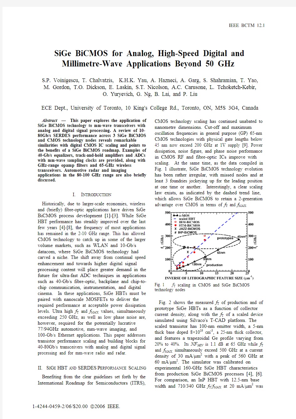
II.S I G E HBT AND SERDES P ERFORMANCE S CALING Benefiting from the clear guidelines set forth by the International Roadmap for Semiconductors (ITRS), CMOS technology scaling has continued unabated to nanometre dimensions. Cut-off and maximum oscillation frequencies in general purpose (GP) 65-nm CMOS technologies with physical gate lengths below 45 nm now exceed 200 GHz at 1V supply [9]. Power dissipation, noise figure, and phase noise performance in CMOS RF and fibre-optic ICs improve with scaling. At the same time, as the data compiled in Fig. 1 illustrate, SiGe BiCMOS technology evolution has been rather irregular, with missed nodes and at least 3 foundries jockeying up for the leading position at one time or another. Interestingly, a clear scaling law exists, as indicated by the dashed trend line, which allows SiGe BiCMOS to retain a 2-generation advantage over CMOS in terms of f T and f MAX .
Fig. 1 f T scaling in CMOS and SiGe BiCMOS technology nodes
Fig. 2 shows the measured f T of production and of prototype SiGe HBTs as a function of collector current density, along with the f T of a scaled device simulated using Silvaco's T-CAD platform. The scaled transistor has 100-nm emitter width, a 5-nm thick base doped 8×1019 cm-3, a 25-nm thick collector, and features a trapezoidal Ge profile varying from 20% to 40%. Its NF MIN is 1.1 dB at 65 GHz while f T and f MAX simultaneously exceed 500 GHz at a current density of 30 mA/μm2 with a peak of 560 GHz at 60 mA/μm2. The simulator was calibrated on experimental 160-GHz SiGe HBT characteristics from production SiGe BiCMOS processes [4], [6]. For comparison, an InP HBT with 12.5-nm base width and 710/340 GHz f T/f MAX at 20 mA/μm2 was
1-4244-0459-2/06/$20.00 ?2006 IEEE.
recently fabricated [10]. These results indicate that a SiGe HBT structure, much like the ones prototyping today, is capable of maintaining the 2× advantage over 45-nm MOSFETs. However, the significant increase in current density with scaling, and slightly higher NF MIN than MOSFETs at comparable f T , remain weak points of SiGe HBTs. Indeed, experimental device [11] and 60-GHz circuit data [12] indicate comparable or lower NF MIN for 90/65-nm MOSFETs than for the best SiGe HBTs.
Fig. 2 f T and NF MIN at 65 GHz vs J c in production [6], prototype [8], and in simulated scaled SiGe HBTs. The simulated structure is shown in the inset.
A fully integrated 5-GHz wireless transceiver and a 10-Gb/s SONET receiver were first reported at MRS in 1998 [13]. These circuits were implemented in an early version of a 0.5μm SiGe BiCMOS process with 45/60-GHz f T /f MAX [1]. The SONET receiver employed E 2CL logic and operated from a -5.2V supply. The first single-chip 10-Gb/s SONET SERDES [14] and a 10-Gb/s Ethernet (10GE) SERDES (Fig. 3) fabricated in 0.35μm [2] and 0.25μm [3] SiGe BiCMOS processes were introduced in December 2000 and the summer of 2001, respectively. Both these ICs rely on simpler ECL families to reduce the supply voltage of the 10-Gb/s circuitry to 3.3V.
The 0.35μm SiGe HBT has an f T of 45 GHz and allows for a 10-GHz latch to be realized with 2-mA tail current and no inductive peaking. The total power dissipation of the SONET SERDES is 2.2 W and includes a VCSEL driver with output swing and pre-emphasis control, laser bias and monitoring circuitry. The output swing and VCSEL modulating current are adjustable over a 3:1 range up to 2×750mV pp and 15mA, respectively [14]. The 10GE SERDES dissipates 3.2 W from 3.3-V, 2.5-V and 1.8-V supplies. It incorporates over 200,000 digital CMOS gates embedded between the analog 10.3-Gb/s and 3.125-Gb/s interfaces (Fig.3). Taking advantage of both SiGe HBT and CMOS scaling across technology nodes, and reducing the number of vertically-stacked transistors, two new generations of this chip have since been ported, first to 180-nm SiGe BiCMOS [4] dissipating about 2 W from 3.3-V and 1.8-V supplies,
and next to 130-nm CMOS, dissipating approximately 1 W from a 1.2-V supply.
The most interesting aspect of this SERDES family is that it demonstrates the benefits of scaling for mixed-signal SiGe BiCMOS products. Scaling leads to an almost linear improvement in jitter, rise/fall times, die area, supply voltage and power dissipation [15]. It also confirms the prediction made in [14] that only at the 130-nm node would CMOS be able to compete with SiGe BiCMOS technology for 10-Gb/s SERDES applications. Indeed, several 10-Gb/s SERDES chips in 130-nm CMOS, including a VCSEL driver [16], have been reported during the last 2 years while 180-nm CMOS solutions could not
compete [17].
Fig. 3 Single-chip 10GE transceiver in 0.25μm SiGe BiCMOS: a) die photograph and b) 10.3-Gb/s output eye diagram (Quake Technologies 2001)
Although a 40-GHz flip-flop [18] and a 60-Gb/s 2:1 MUX [19] have recently been realized in 90-nm CMOS, a 45-GHz flip-flop, as needed for a full-rate 40-Gb/s SONET SERDES with FEC, has only been demonstrated in InP [20] and SiGe BiCMOS technologies [21]-[23]. Scaled 40/80-Gb/s SERDES can now be fabricated in 130-nm SiGe BiCMOS technology [6], operating from 2.5-V supply with similar power dissipation and performance margin (Fig.4) as the first-generation 10GE chip (Fig. 3). This (4-8)× speed increase [23] at comparable power dissipation and cost has been made possible by the 4× improvement in transistor f T /f MAX and by relying on a MOS-SiGe HBT cascode topology and inductive
peaking [23]. The combination of MOSFETs and HBTs on the high-speed path capitalizes on the low V T of nanoscale MOSFETs, the cancellation of Miller capacitance, and on the low gate resistance to improve switching speed over HBT-only logic while reducing the power supply voltage to 2.5 V and 1.8 V [11, 24]. Fig. 5 illustrates the scaling of MOS-HBT cascode inverter delay between production 180-nm and 130-nm SiGe BiCMOS nodes with comparable SiGe HBT performance. The benefits of future scaling to 90-nm BiCMOS are also clearly apparent where the delay reduction from 5.1 ps to 3.3 ps is solely due to replacing 130-nm with 90-nm MOSFETs. The inset shows how emitter-followers (EF) can be employed for level shifting and further increase speed. Note that the optimal delay is achieved when the tail current corresponds to 0.3mA/μm of gate width for the
MOSFETs that make up the differential pair [27].
Fig. 4 2×300mV pp , 80-Gb/s output eye diagram (running for 1 hour) of a 2.5-V, 1.4W transmitter [23] implemented in a 130-nm SiGe BiCMOS process [6].
Fig. 5 Scaling of BiCMOS cascode inverter delay across nodes obtained from measured DC and high-frequency characteristics. All inverters have a gain of 1.5 and a fanout of 1. The impact of the EF stage is not included.
III. A NALOG C IRCUITS
Operational amplifiers (opamps) can be used in GHz-range filters and delta-sigma modulators if their unity gain bandwidth exceeds 10 GHz [25], [26]. The schematic of a fully differential opamp employing a MOS-HBT cascode with cascode p-MOSFET load [25] is shown in Fig. 6. The circuit has an EF output for level-shifting purposes and to reduce the output
impedance. It was implemented in 130-nm and 180-nm generations of SiGe BiCMOS technologies with similar HBT f T /f MAX [25],[26]. The MOS-HBT cascode has speed, linearity and noise advantages over the HBT-HBT cascode. This is the result of the lower input time constant R G ×(C gs +C gd ), better phase margin and concomitant low-noise and high-linearity bias in MOSFETs, as opposed to HBTs. To maximize the unity gain bandwidth, all MOSFETs and HBTs are biased at the peak f MAX current density which, for n-MOSFETs and p-MOSFETs, is approximately 0.2 mA/μm and 0.08 mA/μm, respectively, across technology nodes and foundries [27]. A record unity gain bandwidth of 37 GHz was measured in the 130-nm half-circuit with 10-mA current [25]. Opamp biquad filters (Fig. 7) were fabricated and their performance was compared with that of 2-stage g m -LC bandpass filters based on the same MOS-HBT cascode topology (Fig. 8). The measured transfer characteristics, NF and linearity of both filters are shown in Figs. 9-11. With comparable linearity and power dissipation, the opamp filter occupies 10 times smaller area than the g m
-LC filter.
Fig. 8 Block diagram of 130-nm SiGe BiCMOS g m -LC filter based on a BiCMOS cascode.
IEEE BCTM 12.1
IV. 40-G B /S E QUALIZERS
Production SiGe BiCMOS technology is well-poised to address 45-Gb/s transceivers with equalization. A typical block diagram of an equalizer with analog DSP is shown in Fig. 12. While the FFE block could be realized in 90-nm CMOS, the DFE requires a full-rate 45-GHz flip-flop which is unlikely to be implemented in CMOS with adequate margin
before the 65-nm node.
Fig. 9 Measured biquad and gm-LC filter characteristics for different bias conditions. Measurements of the g m -LC filters with and without an output buffer are provided.
Fig. 10 Measured 50-Ω NF of opamp half-circuit and of differential gm-LC filter.
Fig. 11 Comparison of the measured linearity of two-stage opamp and g m -LC filters operating at 1.2 GHz and 1.9 GHz, respectively.
Fig. 12 Block diagram of electrical equalizer for polarization mode dispersion in optical fibers.
A. Feed Forward Equalizer
Fig. 13 describes the block diagram of a 7-tap 40-Gb/s FFE [28] implemented in a 180-nm SiGe BiCMOS process [4]. A differential, distributed topology is employed which is realized with M6-over-M2 microstrip lines and HBT-cascode taps with gain and sign control. The measured and modelled characteristics of the 9-ft SMA cable used in system-level simulations and experiments are illustrated in Figs. 14-16. The circuit is capable of compensating for more than 20dB loss at 20 GHz. Error-free operation was verified from 5 Gb/s to 40 Gb/s, and
equalized eyes were obtained up to 49 Gb/s [28].
Fig. 13 Schematics of 7-tap FFE implemented in 180-nm SiGe BiCMOS.
Fig. 14 Modeled vs. measured transmission loss of 9-ft
SMA cable.
Fig. 15 Modelled 40-Gb/s equalized eye diagrams as a function of the number of equalizer taps. a) input signal after passing through the SMA cable and output of b) 2-tap, c) 3-tap, d) 7-tap equalizers.
B. 40 Gb/s DFE
The DFE whose block diagram is shown in Fig. 17, was implemented in the same technology [4] with 3.3-V ECL and verified to correctly equalize a PRBS
IEEE BCTM 12.1
passing through a 9-ft SMA cable at data rates from
5 Gb/s to 39.5 Gb/s, Fig.18 [29].
Fig. 16 FFE input/output 40-Gb/s eye diagrams and bathtub.
Fig. 17 1-tap look-ahead DFE architecture.
C. 40 Gb/s Digital Equalizer Blocks
When the technology has adequate speed, a digital DSP solution (Fig. 19) is preferred over an analog one
due to its increased flexibility. In this architecture, the most critical block is the T&H amplifier (Fig. 20), which must simultaneously satisfy broad band, low noise and high linearity requirements. A T&H
amplifier with over 40-GHz bandwidth (Fig. 21) and
4.5-bit linearity was reported in [30].
Fig. 18 39.5-Gb/s DFE input and output eye diagrams after passing through a 9-ft long SMA cable.
Fig. 19 Block diagram of a DSP based fiber optic equalizer.
Fig. 20 Circuit diagram of the track & hold block in 180-nm SiGe BiCMOS [4]. Signals In N and In P are provided by a low-noise, broadband transimpedance amplifier [30].
Fig. 21 Differential output of the T&H amplifier for an
10-GHz sinusoid sampled at 40GHz (70 mV/div) [30]. V. ADC S The high intrinsic speed of both SiGe HBTs [1]-[8] and CMOS [11], [12] transistors provides an excellent
IEEE BCTM 12.1
incentive for the introduction of digital signal processing techniques relying on high oversampling ratios and mm-wave clock frequencies. Such techniques typically require only simple circuit topologies, similar to those used in a fiberoptic SERDES, that can be designed to be robust to process variations, transistor leakage and non-linearity. The 2-GHz bandpass ΔΣ design described in [31] employs the g m -LC transconductor from Fig. 8 and the BiCMOS cascode MSM flip-flop [22] as the 40-GSamples/sec quantizer. The IIP3 test in Fig. 23 shows an SFDR of 61 dB with an ENOB of 8.5 over a 120 MHz band centred at 2 GHz. The 40-Gb/s output stream, reproduced in Fig. 24, can be decimated with
the same 2.5-V CML BiCMOS logic family [22]-[24].
Fig. 22 System level ΔΣ ADC diagram [31].
Fig. 23 IIP3 test for 40-GS/s 2-GHz bandpass ADC.
Fig. 24 ΔΣ bandpass ADC output eye diagram in open loop at 40Gb/s with a 2-GHz sinusoidal input. VI. M ILLIMETRE W AVE T RANSCEIVERS
Figs. 25 and 26 reproduce the schematics and die photos of a 60-GHz WLAN transceiver chip set and of a 65-GHz Doppler sensor with on-die patch antenna [32], [33] implemented in a production 180-nm SiGe BiCMOS process with f T /f MAX of 160 GHz [4]. The transmitter has an image-reject architecture with stagger-tuned, two-stage, lumped poly-phase filters at 5 GHz and at 65 GHz. All three ICs include for the first time a low-phase-noise 60-GHz VCO with 10% tuning range [34] and rely on inductors and transformers to minimize die area. The VCO, downconvert mixer, LNA, and power amplifier employ SiGe HBT cascodes with inductive degeneration to improve isolation and simplify inter-stage matching. The entire design process was conducted using hand analysis and Spectre, as in the 2-10 GHz range [35], while inductors and
Fig. 25 Block diagrams of a) 60-GHz radio transmitter, b) Doppler radar implemented in 180-nm SiGe BiCMOS.
Fig. 26 Die photos of Doppler radar with patch antenna (left) WLAN transmitter (bottom) and receiver (top right).
Fig. 27 shows the measured conversion gain of the WLAN receiver measured on wafer, and of the Doppler sensor with and without the on-die antenna. The Doppler sensor with antenna was tested either by
placing a horn antenna, or a GGB probe at different elevations above the on-die antenna. The double-sideband (DSB) noise figure, typically 12 dB, and the
corresponding single-ended down-conversion gain of the WLAN receiver, 15 dB at 2.5 V, and 20 dB at 3.3 V supply, are compiled in Fig. 28. More than 45 dB of image rejection has been measured in the WLAN
transmitter, Fig. 29.
Fig. 27 Single-ended conversion gain for radar and WLAN receiver with radio IF at 1 GHz and radar IF at 730 MHz. Fig. 28 Measured WLAN receiver gain and noise figure. Fig. 29 SSB WLAN radio transmitter image rejection vs.
IF input power with 61-GHz LO and 5-GHz IF.
Even though prototype SiGe HBTs and production 65-nm MOSFETs [12] now have adequate performance for automotive radar and imaging at 94 GHz [36],[37], on-chip isolation remains a major concern and will influence the choice of system architecture. For example, beyond 100 GHz, antennas are small enough for phase arrays to be integrated in silicon but crosstalk will limit their applicability. Alternatively, rectangular waveguide arrays are reasonably small, have excellent isolation and, in conjunction with finlines, provide more efficient radiation. For mm-wave medical imaging, where arrays of tens of transceivers are required, low (phase) noise [36], isolation and power dissipation are the most important design goals. Fig. 30 reproduces the measured NF MIN at 5 GHz and at 65 GHz in HBTs with f MAX of 200 GHz and 300 GHz, respectively. NF MIN was obtained from Y-parameter measurements as in [35],[39]. The impact of transistor vertical profile scaling on NF MIN is negligible at 5 GHz but becomes significant at 65 GHz. Furthermore, since the transit time through the collector space charge region is significantly larger than the base transit time, correlation between the collector and base shot noise currents increases, pushing the optimum noise current density at mm-waves close to the peak f T/f MAX current density and changing the value of the optimum noise impedance. The latter has important implications for LNA and VCO design, and allowed us to achieve a record phase noise of -101.3 dBc/Hz at 1 MHz from
the 103.6 GHz carrier, as shown in Fig. 31 [36].
Fig. 30 Measurements of NF MIN scaling in SiGe HBTs.
Fig. 31 Measured spectrum, phase noise of 103-GHz VCO.
VII.C ONCLUSIONS
Low-frequency analog figures of merit such as g m/I, g m/g o, lower 1/f noise and the larger f T×BV CEO product remain the main strengths of SiGe HBTs well into the mm-wave regime. However, historical data, moderate volume markets and relentless pressure from more aggressively scaled CMOS point to the importance of pairing next generation 250/500GHz SiGe HBTs with 90-nm CMOS as a viable and economical way to capture all applications demanding fast HBTs and at least some of the 90/65-nm CMOS market. In that scenario the discontinued supply-voltage scaling of 65-nm CMOS will help release most of the pressure off SiGe. Stand-alone SiGe HBT technology, stripped of its CMOS advantage, will have a difficult time competing with InP or CMOS.
A CKNOWLEDGEMENTS
We thank NSERC, Micronet, CITO, Gennum, NORTEL and STM for funding, and STM and Jazz Semiconductor for fabrication. Equipment grants from CFI and OIT, and CAD tools from CMC are also acknowledged. We are grateful to Dan Trepanier of Quake for the 10GE SERDES data, and to Pascal Chevalier and Alain Chantre of STM for 230-GHz HBT discussions. S. Voinigescu would like to thank
Rudy Beerkens, Bernard Sautreuil, Paul Kempf and Marco Racanelli for their support over many years, and his former colleagues at NORTEL and Quake Technologies in Ottawa, Canada.
R EFERENCES
[1] D.L. Harame et al., “Si/SiGe Epitaxial-Base Transistors
–Part II: Process Integration and Analog Applications,”
IEEE Trans. ED, Vol.42, pp. 459-482, 1995.
[2] A. Monroy, et al., “A high performance 0.35μm SiGe
BiCMOS technology for wireless applications,” Proc.
IEEE BCTM, pp.121-124, Sept. 1999.
[3] H. Baudry et al., “High performance 0.25μm SiGe and
SiGe:C HBTs using non-selective epitaxy,” Proc. IEEE
BCTM, pp.52-55, Sept. 2001.
[4] M. Racanelli, et al., “Ultra High Speed SiGe NPN for
advanced BiCMOS technology,” IEEE IEDM Techn.
Digest, pp. 336-339, Dec. 2001.; M. Racanell and P.
Kempf, “SiGe BiCMOS Technology for RF Circuit Applications,” IEEE Trans. ED, Vol.52, pp. 1259-
1270, 2005.
[5] B. Jaganathan, et al. “Self-aligned SiGe NPN
transistors with 285 GHz f MAX and 207 GHz f T in a manufacturable technology,” IEEE Electron Device Lett., Vol.23, No.5, pp.258-260, March. 2002.
[6] M. Laurens et al, “A 150 GHz f T/f MAX 0.13 μm SiGe:C
BiCMOS technology,” Proc. IEEE BCTM, pp.199-202,
Sept. 2003.
[7] T.F. Meister et al., “SiGe Bipolar Technology with
3.9ps gate delay,”IEEE BCTM, pp.103-106, Sept. 2003.
[8] P. Chevalier et al, “300-GHz f MAX self-aligned SiGeC
HBT optimized towards CMOS compatibility,” Proc.
IEEE BCTM, pp.120-123, Oct. 2005.
[9] B. Jagannathan, et al, “RF CMOS for Microwave and
MM-wave Applications,” IEEE SiRF, Techn. Digest.
pp.259-264, Jan. 2006.
[10] W. Hafez et al., “12.5 nm base pseudomorphic
heterojunction bipolar transistors achieving f T=710
GHz and f MAX = 340 GHz,” Appl.Phys.Lett., Vol.87, pp.252109-1/3, Dec. 2005
[11] P. Chevalier et al., “Advanced SiGe BiCMOS and
CMOS Platforms for Optical and mm-wave ICs,” IEEE
CSICS, San Antonio, Nov. 2006.
D. Grindberg, “Silicon Heterostructure Handbook,”
pp.4.5-439-457 Taylor & Francis, 2006.
[12] T. Yao, et al., “60-GHz PA and LNA in 90-nm RF-
CMOS,” IEEE RFIC Symposium Digest, pp. 147-150, June 2006.
D. Alldred et al. “A 1.2V, 60GHz radio receiver with
on-chip transformers and inductors in 90nm CMOS,”
IEEE CSICS, San Antonio, Nov. 2006.
[13] R. Hadaway, et al., “Application of SiGe HBTs to
Datacom and Wireless,” MRS, April, 1998.
[14] S.P. Voinigescu et al., “Circuits and Technologies for
Highly Integrated Optical Networking ICs at 10Gb/s to
40Gb/s,” Proc. IEEE CICC, pp.331-338, May 2001.
[15] D. Trepanier, IEEE CSICS Panel Nov. 2005.
[16] S. Rabii, et al., “An Integrated VCSEL Driver for 10
Gb/s Ethernet in 0.13μm CMOS,” IEEE ISSCC Digest,
pp.246-247, Feb. 2006.
[17] J. Cao et al, “OC-192 Receiver in Standard 0.18μm
CMOS,” ISSCC Digest, pp.250-251, Feb. 2002.
[18] T. Chalvatzis, et al., “A 40Gb/s Decision Circuit in
90-nm CMOS,” ESSCIRC, Montreux, Sept. 2006. [19] D. Kehrer et al., “A 60Gb/s 2:1 Selector in 90nm
CMOS,” IEEE CSICS Digest, pp.105-108, Oct. 2004. [20] A. Hendarman, et al., “STS-768 Multiplexer With Full-
Rate Output Data Retimer in InP HBT,” IEEE J.Solid-
State Circuits, Vol.38, pp.1497-1503, Sept. 2003. [21] M. Meghelli, “A 108Gb/s 4:1 Multiplexer in 0.13 μm
SiGe-Bipolar Technology,” ISSCC Digest, pp.236-237,
Feb. 2004.
[22] T.O. Dickson, et al., “A 2.5-V, 45-Gb/s Decision
Circuit Using SiGe BiCMOS Logic,” IEEE J. Solid-
State Circuits, Vol.40, No.4, pp.994-1003, 2005.
[23] T.O. Dickson and S. P. Voinigescu., “Low-power
circuits for a 10.7-to-86 Gb/s 80-Gb/s serial transmitter
in 130-nm SiGe BiCMOS,” IEEE CSICS, Nov. 2006. [24] E. Laskin and S.P. Voinigescu, “A 60 mW per Lane, 4
× 23-Gb/s 27-1 PRBS Generator,” IEEE CSICS, Techn.
Digest, pp.192-195, Nov. 2005.
[25] S.P. Voinigescu, et al., “Design Methodology and
Applications of SiGe BiCMOS Cascode Opamps with
up to 37-GHz Unity Gain Bandwidth,” IEEE CSICS,
Techn. Digest, pp.283-286, Nov. 2005.
[26] G. Ng, et al., “1 GHz Opamp-Based Bandpass Filter,”
IEEE SiRF, Techn. Digest. pp.369-372, Jan. 2006. [27] T.O. Dickson et al., “The Invariance of Characteristic
Current Densities in Nanoscale MOSFETs and its
Impact on Algorithmic Design Methodologies and Design Porting of Si(Ge) (Bi)CMOS High-Speed Building Blocks,” IEEE J. S-St. Circuits, Aug. 2006. [28] A. Hazneci and S. P. Voinigescu, “49-Gb/s, 7-Tap
Transversal Filter in 0.18μm SiGe BiCMOS for Backplane Equalization,” IEEE CSICS, pp.101-104,
Oct.2004.
[29] A. Garg, et al., “A 1-Tap 40-Gbs Lookahead Decision
Feedback Equalizer in 0.18μm SiGe BiCMOS Technology,” IEEE CSICS, pp.37-41, Nov.2005. [30] S. Shahramian, et al., “A 40-GSamples/Sec Track &
Hold Amplifier in 0.18μm SiGe BiCMOS Technology,” IEEE CSICS, pp.101-104, Nov. 2005. [31] T. Chalvatzis and S. P. Voinigescu, “A Low-Noise
40-GS/s Continuous-Time Bandpass ΔΣ ADC Centered at 2GHz,” IEEE RFIC Symposium Digest, pp.
323-326, June 2006.
[32] M. Gordon, et al.,”65-GHz Receiver in SiGe BiCMOS
Using Monolithic Inductors and Transformers” IEEE
SiRF Techn. Digest. pp.265-268, Jan. 2006.
[33] T. Yao, et al., “65GHz Doppler Radar Transceiver with
On-Chip Antenna in 0.18μm SiGe BiCMOS,” IEEE
IMS Digest, pp.1493-1496, June 2006.
[34] C. Lee, et al., “SiGe BiCMOS 65-GHz BPSK
Transmitter and 30 to 122 GHz LC-Varactor VCOs
with up to 21% Tuning Range,” IEEE CSICS, Technical Digest, pp.179-182, Oct. 2004.
[35] S.P. Voinigescu et al, “A scalable high-frequency noise
model for bipolar transistors with application to optimal transistor sizing for low-noise amplifier design,” IEEE J. Solid-State Circuits, vol. 32, pp.
1430-1438, Sept. 1997.
[36] S.T. Nicolson, et al, “Design and Scaling of SiGe
BiCMOS VCOs Operating near 100 GHz,” IEEE
BCTM 2006.
[37] E. Laskin et al. “Low-Power, Low-Phase Noise SiGe
HBT Static Frequency Divider Topologies up to 100 GHz,” IEEE BCTM 2006.
[38] T.O. Dickson, S.P. Voinigescu, “SiGe BiCMOS
Topologies for Low-Voltage Mm-Wave Voltage-
Controlled Oscillators and Frequency Dividers,” IEEE
SiRF, Techn. Digest. pp.273-276, Jan. 2006.
[39] K.H.K. Yau and S.P. Voinigescu, “Modeling and
Extraction of SiGe HBT Noise Parameters from Measured Y-Parameters and Accounting for Noise
Correlation,”IEEE SiRF Digest. pp.226-229, Jan. 2006.
IEEE BCTM 12.1
电路原理图设计步骤
电路原理图设计步骤 1.新建一张图纸,进行系统参数和图纸参数设置; 2.调用所需的元件库; 3.放置元件,设置元件属性; 4.电气连线; 5.放置文字注释; 6.电气规则检查; 7.产生网络表及元件清单; 8.图纸输出. 模块子电路图设计步骤 1.创建主图。新建一张图纸,改名,文件名后缀为“prj”。 2.绘制主图。图中以子图符号表示子图内容,设置子图符号属性。 3.在主图上从子图符号生成子图图纸。每个子图符号对应一张子图图纸。 4.绘制子图。 5.子图也可以包含下一级子图。各级子图的文件名后缀均是“sch”。 6.设置各张图纸的图号。 元件符号设计步骤 1.新建一个元件库,改名,设置参数; 2.新建一个库元件,改名; 3.绘制元件外形轮廓; 4.放置管脚,编辑管脚属性; 5.添加同元件的其他部件; 6.也可以复制其他元件的符号,经编辑修改形成新的元件; 7.设置元件属性; 8.元件规则检查; 9.产生元件报告及库报告; 元件封装设计步骤 1.新建一个元件封装库,改名; 2.设置库编辑器的参数; 3.新建一个库元件,改名; 4.第一种方法,对相似元件的封装,可利用现有的元件封装,经修改编辑形成; 5.第二种方法,对形状规则的元件封装,可利用元件封装设计向导自动形成; 6.第三种方法,手工设计元件封装: ①根据实物测量或厂家资料确定外形尺寸; ②在丝印层绘制元件的外形轮廓; ③在导电层放置焊盘; ④指定元件封装的参考点 PCB布局原则 1.元件放置在PCB的元件面,尽量不放在焊接面; 2.元件分布均匀,间隔一致,排列整齐,不允许重叠,便于装拆; 3.属同一电路功能块的元件尽量放在一起;
原理图元件库的设计步骤(精)
原理图元件库的设计步骤 一. 了解欲绘制的原理图元件的结构 1. 该单片机实际包含40只引脚,图中只出现了38只, 有两只引脚被隐藏,即电源VCC(Pin40和GND(Pin20。 2. 电气符号包含了引脚名和引脚编号两种基本信息。 3. 部分引脚包含引脚电气类型信息(第12脚、第13脚、第32至第39脚。 4. 除了第18脚和第19脚垂直放置,其余水平放置。由于VCC及GND隐藏,所以放置方式可以任意。 5. 一些引脚的名称带有上划线及斜线,应正确标识。
二. 新建集成元件库及电气符号库 1. 在D盘新建一个文件夹D:/student 2. 建立一个工程文件,选择File/New/Project/Integrated Library,如:Dong自制元件库.LibPkg 3. 新建一个电气符号库,选择File/New/Library/Schematic Library,如:Dong自制元件库.SchLib 4. 追加原理图元件 在左侧的SCH Library标签中,点击库元件列表框(第一个窗口下的Add(追加按钮,弹出New Component Name对话框,追加一个原理图元件,输入8051并确认,8051随即被添加到元件列表框中。 三. 绘制原理图元件 1. 绘制矩形元件体 矩形框的左上角定位在原点,则矩形框的右下脚应位于(130,-250。 注意:图纸设置中各Grids都设为10mil。 2. 放置引脚 (1P0.0~P0.7的放置及属性设置 单击实用工具面板的引脚放置工具图标,并按Tab键,系统弹出【引脚属性】对话框: 【Display Name显示名称】文本框中输入“P0.0”; 【Designator标识符】文本框中输入“39”;
原理图和PCB的设计规范
一.PCB设计规范 1、元器件封装设计 元件封装的选用应与元件实物外形轮廓,引脚间距,通孔直径等相符合。元件外框丝印统一标准。 插装元件管脚与通孔公差相配合(通孔直径大于元件管脚直径8-20mil),考虑公差可适当增加。建立元件封装时应将孔径单位换算为英制(mil),并使孔径满足序列化要求。插装元件的孔径形成序列化,40mil以上按5mil递加,即40mil,45mil,50mil……,40mil以下按4mil递减,即36mil,32mil,28mil……。 2、PCB外形要求 1)PCB板边角需设计成(R=1.0-2.0MM)的圆角。 2)金手指的设计要求,除了插入边按要求设计成倒角以外,插板两侧边也应设计成(1-1.5)X45度的倒角或(R1-1.5)的圆角,以利于插入。 1.布局 布局是PCB设计中很关键的环节,布局的好坏会直接影响到产品的布通率,性能的好坏,设计的时间以及产品的外观。在布局阶段,要求项目组相关人员要紧密配合,仔细斟酌,积极沟通协调,找到最佳方案。 器件转入PCB后一般都集中在原点处,为布局方便,按合适的间距先把 所有的元器件散开。 2)综合考虑PCB的性能和加工效率选择合适的贴装工艺。贴装工艺的优先顺序为: 元件面单面贴装→元件面贴→插混装(元件面插装,焊接面贴装一次波峰成形); 元件面双面贴装→元件面插贴混装→焊接面贴装。 1.布局应遵循的基本原则 1.遵照“先固后移,先大后小,先难后易”的布局原则,即有固定位 置,重要的单元电路,核心元器件应当优先布局。
2.布局中应该参考原理图,根据重要(关键)信号流向安排主要元器 件的布局。 3.布局应尽量满足以下要求:总的连线尽可能短,关键信号线最短, 过孔尽可能少;高电压,大电流信号与低电压,小电流弱信号完全分开; 模拟与数字信号分开。 4.在满足电器性能的前提下按照均匀分布,重心平衡,美观整齐的标 准优化布局。 5.如有特殊布局要求,应和相关部门沟通后确定。 2.布局应满足的生产工艺和装配要求 为满足生产工艺要求,提高生产效率和产品的可测试性,保持良好的可维护性,在布局时应尽量满足以下要求: 元器件安全间距(如果器件的焊盘超出器件外框,则间距指的是焊盘之 间的间距)。 1.小的分立器件之间的间距一般为0.5mm,最小为0.3mm,相邻器件 的高度相差较大时,应尽可能加大间距到0.5mm以上。如和IC (BGA),连接器,接插件,钽电容之间等。 2.IC、连接器、接插件和周围器件的间距最好保持在1.0mm以上, 最少为0.5mm,并注意限高区和禁止摆放区的器件布局。 3.安装孔的禁布区内无元器件。如下表所示 4.高压部分,金属壳体器件和金属件的布局应在空间上保证与其它 器件的距离满足安规要求。
硬件电路原理图设计审核思路和方法
硬件电路原理图设计审核思路和方法 1、详细理解设计需求,从需求中整理出电路功能模块和性能指标要 求; 2、根据功能和性能需求制定总体设计方案,对CPU进行选型,CPU 选型有以下几点要求: a)性价比高; b)容易开发:体现在硬件调试工具种类多,参考设计多,软件资源丰富,成功案例多; c)可扩展性好; 3、针对已经选定的CPU芯片,选择一个与我们需求比较接近的成功 参考设计,一般CPU生产商或他们的合作方都会对每款CPU芯片做若干开发板进行验证,比如440EP就有yosemite开发板和 bamboo开发板,我们参考得是yosemite开发板,厂家最后公开给用户的参考设计图虽说不是产品级的东西,也应该是经过严格验证的,否则也会影响到他们的芯片推广应用,纵然参考设计的外围电路有可推敲的地方,CPU本身的管脚连接使用方法也绝对是值得我们信赖的,当然如果万一出现多个参考设计某些管脚连接方式不同,可以细读CPU芯片手册和勘误表,或者找厂商确认;另外在设计之前,最好我们能外借或者购买一块选定的参考板进行软件验证,如果没问题那么硬件参考设计也是可以信赖的;但要注意一点,现在很多CPU 都有若干种启动模式,我们要选一种最适合的启动模式,或者做成兼容设计;
4、根据需求对外设功能模块进行元器件选型,元器件选型应该遵守 以下原则: a)普遍性原则:所选的元器件要被广泛使用验证过的尽量少使用冷偏芯片,减少风险; b)高性价比原则:在功能、性能、使用率都相近的情况下,尽量选择价格比较好的元器件,减少成本; c)采购方便原则:尽量选择容易买到,供货周期短的元器件; d)持续发展原则:尽量选择在可预见的时间内不会停产的元器件;e)可替代原则:尽量选择pin to pin兼容种类比较多的元器件;f)向上兼容原则:尽量选择以前老产品用过的元器件; g)资源节约原则:尽量用上元器件的全部功能和管脚; 5、对选定的CPU参考设计原理图外围电路进行修改,修改时对于每 个功能模块都要找至少3个相同外围芯片的成功参考设计,如果找到的参考设计连接方法都是完全一样的,那么基本可以放心参照设计,但即使只有一个参考设计与其他的不一样,也不能简单地少数服从多数,而是要细读芯片数据手册,深入理解那些管脚含义,多方讨论,联系芯片厂技术支持,最终确定科学、正确的连接方式,如果仍有疑义,可以做兼容设计;这是整个原理图设计过程中最关键的部分,我们必须做到以下几点: a)对于每个功能模块要尽量找到更多的成功参考设计,越难的应该越多,成功参考设计是“前人”的经验和财富,我们理当借鉴吸收,站在“前人”的肩膀上,也就提高了自己的起点;
电源设计原理图每个元器件该如何选择
电源设计原理图每个元器件该如何选择 原理图FS1由TR1(热敏VDR1(突波吸收器)当雷极发生时,可能会损坏零件,进而影响Power的正常动作,所以必须在靠AC输入端(Fuse之后),加上突波吸收器来保护Power(一般常用07D471K),但若有价格上的考虑,可先忽略不装。CY1,CY2(Y-Cap)Y-Cap一般可分为Y1及Y2电容,若AC Input有FG(3 Pin)一般使用Y2- Cap ,AC Input若为2Pin(只有L,N)一般使用Y1-Cap,Y1与Y2的差异,除了价格外(Y1较昂贵),绝缘等级及耐压亦不同(Y1称为双重绝缘,绝缘耐压约为Y2的两倍,且在电容的本体上会有“回”符号或注明Y1),此CX1(X-Cap)、RX1X-Cap为防制EMI零件,EMI可分为ConducLF1(Common Choke)EMI防制零件,主要影响Conduction 的中、低频段,设计时必须同时考虑EMI特性及温升,以同样尺寸的Common Choke而言,线圈数愈多(相对的线径愈细),EMI防制效果愈好,但温升可能较高。BD1(整流C1(滤波电容)由C1的大小(电容值)可决定变压器计算中的Vin(D2(辅助电源二极管)整流二极管,一般常用FR105(1A/600V)或BYT42M(1A/1000V),两者主要差异:R10(辅助电源电阻)主要用于调整PWM IC的VCC电压,以目前使用的3843而言,设计时VCC必须大于8.4V(Min. Load 时),但为考虑输出短路的情况,VCC电压不可设计的太高,以免当输出短路时不保护(或输入瓦数过大)。C7(滤波电容)辅助电源的滤波电容,提供PWM IC较稳定的直流电压,一般使用100uf/25V电容。Z1(Zener 二极管)当回授失效时的R2(启动电阻)提供3843第一次启动的路径,第一次启动时透过R2对C7充电,以提供3843 VCC所需的电压,R2阻值较大时,turn on的时间较长,但短路时Pin瓦数较小,R2阻值较小时,turn on的时间较短,短路时Pin瓦数较大,一般使用220KΩ/2W M.O。R4 (Line Compensation)高、低压补偿用,使3843 Pin3脚在90V/47Hz及264V/63Hz接近一致(一般使用750KΩ~1.5MΩ1/4W之间)。R3,C6,D1 (Snubber)此三个零件组成Snubber,调整Snubber的目的:1.当Q1 off瞬间会有Spike产生,调整Snubber可以确保Spike不会超过Q1的耐压值,2.调整Snubber可改善EMI.一般而言,D1使用1N4007(1A/1000V)EMI特性会较好.R3使用2W M.O.电阻,C6的耐压值以两端实际压差为准(一般使用耐压500V的陶质电容)。Q1(N-MOS)
原理图元器件的制作
原理图元器件的制作 一、实验目的 1.掌握DXP2004 原理图元件库文件的创建方法。 2.掌握自建原理图元件库的管理方法和新器件的制作方法 二、实验仪器 计算机、DXP 2004软件 三、实验任务 1. 创建原理图元件库文件 2. 制作新的元器件 3. 把系统Miscellaneous Devices.IntLib库和Miscellaneous Connectors.IntLib库中常用的电阻、电容、二级管、三极管、开关、接插件等元件复制到创建的原理图元件库文件中。 四、实验步骤 4.1创建原理图元件库文件 (1)启动DXP2004软件,打开工程项目文件。创建原理图元件库文件的方法有两种。 方法一:执行菜单File/New/Library/Schematic Library。 方法二:在工程项目工作面板中,将鼠标移到电话接听器.PRJPCB处,点击右键,选择Add New to Project/Schematic Library,如图1所示。 图1 创建原理图元件库文件
执行了原理图元件库文件命令后,在项目工作面板上就多了一个Schlib1.SchLib文件,如图2所示。 图2新建的原理图元件库文件 (2)保存文件。执行菜菜单File/Save命令,或者将鼠标移到图2所示的Schlib1.SchLib处,点击右键,选择Save,进入保存文件对话框,如下图3所示。将文件命名为MYLIB,点击保存按钮,就可以完成文件保存。 图3 原理图元件库文件保存对话框 (3)打开原理图元件库编辑管理器。点击图2所示的SCH Library按钮,或者执行菜单View/WorkSpace Pannels/SCH/SCH Library命令,进入原理图元件库编辑管理器。原理图元件的
Cadence原理图设计简介
原理图设计简介 本文简要介绍了原理图的设计过程,希望能对初学者有所帮助。 一.建立一个新的工程 在进行一个新的设计时,首先必须利用Project Manager 对该设计目录进行配置,使该目录具有如下的文件结构。 所用的文件库 信息。 Design directory 启动Project Manager Open: 打开一个已有Project . New :建立一个新的Project . 点击New 如下图: cadence 将会以你所填入的project name 如:myproject 给project file 和design library 分别命
名为myproject.cpm和myproject.lib 点击下一步 Available Library:列出所有可选择的库。包括cadence自带库等。Project Library:个人工程中将用到的所有库。如myproject_lib 点击下一步 点击下一步
点击Finish完成对设计目录的配置。 为统一原理图库,所有共享的原理图库统一放在CDMA硬件讨论园地----PCB设计专栏内。 其中:libcdma 目录为IS95项目所用的器件库。 libcdma1目录为IS95项目之后所用的器件库。 每台机器上只能存放一套共享的原理图库,一般指定放在D:盘的根目录下, 即:D:\libcdma , D:\libcdma1 ... * 注意:设计开始时,应该首先将机器上的库与共享的原理图库同步。 下面介绍如何将共享库加入到自己的工程库中。 点击Setup 点击Edit 编辑cds.lib文件。添入以下语句: define libcdma d:\libcdma define libcdma1 d:\libcdma1 则库libcdma , libcdma1被加入Availiable Library 项内。如下图:
常用元器件的原理图符号和元器件封装
常用元器件的原理图符号和元器件封装 一、元器件封装的类型 元器件封装按照安装的方式不同可以分成两大类。 (1)直插式元器件封装。 直插式元器件封装的焊盘一般贯穿整个电路板,从顶层穿下,在底层进行元器件的引脚焊接,如图F1-1所示。 图F1-1直插式元器件的封装示意图 典型的直插式元器件及元器件封装如图F1-2 所示。 图F1-2直插式元器件及元器件封装 (2)表贴式元器件封装。 表贴式的元器件,指的是其焊盘只附着在电路板的顶层或底层,元器件的焊接是在装配元器件的工作层面上进行的,如图F1-3所示。 焊盘贯穿整个电路板
Protel 99SE 基础教程2 图F1-3表贴式元器件的封装示意图 典型的表贴式元器件及元器件封装如图F1-4 所示。 图F1-4表贴式元器件及元器件封装 在PCB 元器件库中,表贴式的元器件封装的引脚一般为红色,表示处在电路板的顶层(Top Layer )。 二、常用元器件的原理图符号和元器件封装 在设计PCB 的过程中,有些元器件是设计者经常用到的,比如电阻、电容以及三端稳压源等。在Protel 99SE 中,同一种元器件虽然相同电气特性,但是由于应用的场合不同而导致元器件的封装存在一些差异。前面的章节中已经讲过,电阻由于其负载功率和运用场合不同而导致其元器件的封装也多种多样,这种情况对于电容来说也同样存在。因此,本节主要向读者介绍常用元器件的原理图符号和与之相对应的元器件封装,同时尽量给出一些元器件的实物图,使读者能够更快地了解并掌握这些常用元器件的原理图符号和元器件封装。 (1)电阻。 电阻器通常简称为电阻,它是一种应用十分广泛的电子元器件,其英文名字为“Resistor ”,缩写为“Res ”。 电阻的种类繁多,通常分为固定电阻、可变电阻和特种电阻3大类。 固定电阻可按电阻的材料、结构形状及用途等进行多种分类。电阻的种类虽多,但常用的电阻类型主要为RT 型碳膜电阻、RJ 型金属膜电阻、RX 型线绕电阻和片状电阻等。 固定电阻的原理图符号的常用名称是“RES1”和“RES2”,如图F1-5(a )所示。常用的引脚封装形式为AXIAL 系列,包括AXIAL-0.3、AXIAL-0.4、AXIAL-0.5、AXIAL-0.6、AXIAL-0.7、AXIAL-0.8、AXIAL-0.9和AXIAL-1.0 等封装形式,其后缀数字代表两个焊盘的间焊盘只附着在电路板的顶层或底层
原理图原件库及元件的建立
E原理图原件库及元件的建立 复习:原理图绘制的基本步骤包括哪些?应该注意什么? 重点:1 创建原理图元件库文件 2 绘制原理图元件符号 3 编辑原理图元件符号 4 元件库文件管理 一、新建原理图元件库文件 1、原理图元件库文件的扩展名是.Lib。以将文件建在Documents文件夹下为例: ①打开一个设计数据库文件。 ②在右边的视图窗口打开Documents文件夹。 ③在窗口的空白处单击鼠标右键,在弹出的快捷菜单中选择New,系统弹出New Document对话框。 ④在New Document对话框中选择Schematic Library Document图标。 ⑤单击Ok按钮。 说明:“打开原理图元件库;原理图元件库编辑器界面介绍”具体操作见课件及结合软件操作详细讲解。 2、重点介绍:Components区域;Part 区域中的按钮;Group区域;功能及操作。 二、创建新的原理图元件符号 1、元件绘制工具 在元件库编辑器中,常用的工具栏是SchLib Drawing Tools工具栏。 2、IEEE符号说明 Protel 99 SE提供了IEEE符号工具栏,用来放置有关的工程符号。 3、例题:绘制一个新的元器件符号:AT89C51单片机;DS1302时钟芯片;LCD1602字符点阵液晶显示
操作步骤: (1)打开一个自己建的原理图元件库文件,如SchLib1.Lib。 (2)单击工具栏中的按钮,或执行菜单命令Tools|New Component,系统弹出New Component Name 对话框。 (3)对话框中的COMPONENT_1是新建元件的默认元件名,将其改为DS1302后单击Ok按钮,屏幕出现一个新的带有十字坐标的画面。 (4)设置栅格尺寸:执行菜单命令Options|Document Options,系统弹出Library Editor Workspace对话框,设置锁定栅格尺寸,即Snap的值为5。 (5)按Page Up键,放大屏幕,直到屏幕上出现栅格。 (6)单击工具栏上矩形按钮,在十字坐标第四象限靠近中心的位置,绘制元件外形,尺寸为11格×9格。(7)放置引脚:单击工具栏中的按钮,按Tab键系统弹出Pin属性设置对话框。 Pin属性设置对话框中各选项含义: ●Name:引脚名。如P1.0等。 ●Number:引脚号。每个引脚必须有,如1、2、3。 ●X-Location、Y-Location:引脚的位置。 ●Orientation:引脚方向。共有0 Degrees、90 Degrees、180 Degrees、270 Degrees四个方向。 ●Color:引脚颜色。 ●Dot:引脚是否具有反相标志。√表示显示反相标志。 ●Clk:引脚是否具有时钟标志。√表示显示时钟标志。 ●Electrical :引脚的电气性质。其中:Input:输入引脚;IO:输入/输出双向引脚;Output:输出;Open Collector:集电极开路型引脚;Passive:无源引脚(如电阻电容的引脚);HiZ:高阻引脚;Open Emitter:射极输出;Power:电源(如VCC和GND) ●Hidden:引脚是否被隐藏,√表示隐藏。 ●Show Name:是否显示引脚名,√表示显示。 ●Show Number:是否显示引脚号,√表示显示。 ●Pin:引脚的长度。 ●Selection:引脚是否被选中。 其中电气性能除第10引脚GND和第20引脚Vcc外均选择为Passive,引脚长度为20。 GND和Vcc的电气性能选择Power,引脚长度为20。 (8)定义元件属性,执行菜单命令Tools|Description,系统弹出Component Text Fields对话框,在对话框中设置Default Designator:U?(元件默认编号)和元件的封装形式DIP20。 (9)单击主工具栏上的保存按钮,保存该元件。 4、绘制复合元件中的不同单元:具体操作见课件。 三、自制元器件的应用: 绘制单片机与1602的连接图,重点强调自制元器件的使用方法及注意事项。 总结:学会自制原理图元件的操作,会管理元件库,特别是学会使用自己的元器件。 作业: 1、绘制下图中的各个元器件并绘制原理图。
常见SPDT继电器的原理图元件和封装设计
常见SPDT继电器的原理图和封装设计 1、5引脚SPDT继电器的原理图和封装设计 DXP系统提供的5引脚SPDT继电器原理图符号见图1,图中1号引脚为COM公共端,2号引脚为NC(Normal Close常闭),3号引脚为NO(Normal Open)常开,4、5号引脚为无极性线圈。默认的封装是DIP-P5/X1.65,该封装长35.5mm*宽21.6mm,尺寸比较大,在教育机器人驱动控制时一般使用小功率如HHC66A(T73) 继电器,但是一般生产厂家给出的器件说明书中的电气示意图和封装参数都没有标示引脚编号,如果设计时没有实际器件,在使用时从网络上难以找到完整信息,需要综合比较才能得到正确的设计。 图1 DXP2004系统给出的5引脚SPDT继电器原理图符号和封装在进行电路设计时,必须要有实物才能设计正确的元件封装。下面比较两个不同厂家生产的5引脚SPDT继电器,进行原理图元件和元件封装的设计。 图2 5引脚SPDT继电器的封装设计比较 比较两个厂家相同尺寸封装的5引脚SPDT继电器,从元件实物图片看,汇港继电器是左边三个引脚(图a),底面标示了各引脚的电气属性,没有引脚编号,给引脚按图示进行编号,得到电气特性和元件封装(见图c),松乐继电器是右边三个引脚(图b),给出了电气连接示意图和1、3号引脚编号,按此编号对所有引脚统一编号,得到电气特性和元件
封装(见图d),比较(c)(d)发现两种继电器的电气特性是一致的,封装是中心对称的,常开引脚是左上角或右下角的那个引脚,说明两种不同厂家生产出来的继电器可以通用,并使用统一的原理图元件和封装(设计封装时的尺寸位置根据元件说明书提供的参数确定)。 (a)原理图库元件RELAY-SPDT 5PIN (b)元件库封装5PIN-RELAY—SPDT 图3 自建库的5引脚SPDT继电器原理图符号和封装 图4 HHC66A(T73)继电器封装参数及电气连接图 2、6引脚SPDT继电器的原理图和封装设计 汇港继电器HRS1H-S-DC12V 汇科继电器HK4100F-DC5V-SH 超小型6引脚SPDT继电器,安装尺寸(单位mm):长15.5*10.5*11.8,引脚长度
开关电源原理图各元件功能详解
CX1(X-Cap)、RX1: 电源原理图--每个元器件的功能详解! 由变压器计算得到 lin 值,以此lin 值(0.42A )可知使用公司共享料 2A/250V , 设计时亦须考虑 Pin (max )时的lin 是否会超过保险丝的额定值。 TR1(热敏电阻): 电源启动的瞬间,由于 C1(一次侧滤波电容)短路,导致lin 电流很大,虽 然时间很短暂,但亦可能对 Power 产生伤害,所以必须在滤波电容之前加装一 个热敏电阻,以限制幵机瞬间 lin 在Spec 之内(115V/30A ,230V/60A ),但因热 敏电阻亦会消耗功率,所以不可放太大的阻值 (否则会影响效率),一般使用 5 Q -10 Q 热敏,若 C1电容使用较大的值,则必须考虑将热敏电阻的阻值变大 (一 般使用在大瓦数的 Power 上)。 VDR1(突波吸收器): 当雷极发生时,可能会损坏零件,进而影响 Power 的正常动作,所以必须在 靠AC 输入端(Fuse 之后),加上突波吸收器来保护 Power ( 一般常用07D471K ), 但若有价格上的考虑,可先忽略不装。 CY1,CY2(Y-Cap): Y-Cap 一般可分为 Y1及Y2电容,若ACInput 有FG (3 Pin ) —般使用 Y2- Cap , ACInput 若为2Pin (只有L ,N )一般使用 Y1-Cap ,Y1与Y2的差异,除了价格外 (Y1较昂贵),绝缘等级及耐压亦不同 (Y1称为双重绝缘,绝缘耐压约为 Y2的两 倍,且在电容的本体上会有 “回”符号或注明 Y1),此电路蛭 蠪G 所以使用Y2-Cap , Y-Cap 会影响EMI 特性,一般而言越大越好,但须考虑漏电及价格问题,漏电 ( Leakage