A 2.4 GHz Fully Integrated Cascode-Cascade CMOS Doherty Power Amplifier

A 2.4GHz Fully Integrated Cascode-Cascade
CMOS Doherty Power Ampli?er
Li-Yuan Yang,Hsin-Shu Chen ,Member,IEEE ,and Yi-Jan Emery Chen ,Senior Member,IEEE
Abstract—This letter presents the ?rst CMOS Doherty power ampli?er (PA)fully integrated on chip.The “cascode-cascade”am-pli?er architecture is proposed to get rid of the bulky power splitter and facilitate the integration.The quarter wavelength transmis-sion lines are replaced by the lumped component networks such that the whole ampli?er circuit can be squeezed into the die size of
1.97 1.4mm
2.Fabricated in
0.18m CMOS technology,the 3.3V PA achieves 12dB power gain.The measured output power and power added ef?ciency (PAE)at 1dB are more than 21dBm and 14%,respectively.The PAE at 7dB back-off from 1dB is above 10%and the PAE degradation is less than 29%.
Index Terms—CMOS,ef?ciency,fully integrated,orthogonal frequency division multiplexing (OFDM),peak-to-average power ratio (PAPR),power ampli?er (PA),power back-off.
I.I NTRODUCTION
W
ITH the thirst for high data-rate transmission,Orthog-onal Frequency Division Multiplexing (OFDM)modu-lation technique,which is robust against multi-path fading [1],is widely used in modern high-speed wireless communication sys-tems.However,the multi-carrier characteristic of OFDM sig-nals leads to large peak-to-average power ratio (PAPR)and dy-namic range [2].The high PAPR results in a particular design challenge for radio frequency (RF)power ampli?ers (PAs)be-cause high power ef?ciency is usually achieved when PAs de-liver peak power.The ef?ciency will degrade dramatically when RF PAs operate in back-off region.Unfortunately,the OFDM systems transmit signals at the vicinity of average power level most of the time,so the ef?ciency of RF PAs becomes a signif-icant issue.
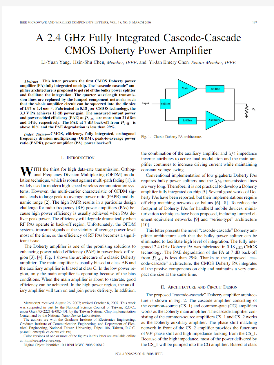
The Doherty ampli?er is one of the promising solutions to enhancing power-added ef?ciency (PAE)in power back-off re-gion [3],[4].Fig.1shows the architecture of a classic Doherty ampli?er.The main ampli?er is usually biased at class AB and the auxiliary ampli?er is biased at class C.In the low power re-gion,only the main ampli?er is operating because of the bias conditions.When the main ampli?er is about to saturate,good ef?ciency can be achieved.In the high power region,the auxil-iary ampli?er will turn on and join power delivery.In addition,
Manuscript received August 26,2007;revised October 8,2007.This work was supported in part by the National Science Council of Taiwan,R.O.C.,under Grant 95-2221-E-002-401,by the Taiwan National Chip Implementation Center,and by the National Nano Device Laboratories.
The authors are with the Graduate Institute of Electronics Engineering,Graduate Institute of Communication Engineering,and Department of Elec-trical Engineering,National Taiwan University,Taipei 106,Taiwan,R.O.C.(e-mail:emery@https://www.360docs.net/doc/6213842524.html,.tw).
Color versions of one or more of the ?gures in this letter are available online at https://www.360docs.net/doc/6213842524.html,.
Digital Object Identi?er
10.1109/LMWC.2008.916812
Fig.1.Classic Doherty PA architecture.
the combination of the auxiliary ampli?er
and
impedance inverter attributes to active load modulation and the main am-pli?er continues to increase driving current while maintaining constant voltage swing.
Conventional implementation of low gigahertz Doherty PAs
requires bulky power splitters and
the
transmission lines are very long.Therefore,it is not practical to develop a Doherty ampli?er fully integrated on chip [5].Several good works of Do-herty PAs have been reported,but their implementations require off-chip matching networks or baluns [6]–[8].To reduce the footprint of Doherty PAs for handheld mobile devices,minia-turization techniques have been proposed,including lumped el-ement equivalent networks [9]and “series-type”architecture [10].
This letter presents the novel “cascode-cascade”Doherty am-pli?er architecture such that the bulky power splitter can be eliminated to facilitate high level of integration.The fully inte-grated 2.4GHz Doherty PA was fabricated in
0.18
CMOS technology.The PAE degradation of the PA at 7dB back-off
from
is less than 29%.Thanks to the proposed “cas-code-cascade”architecture,the CMOS Doherty PA integrates all the passive components on chip and maintains a very com-pact die size at the same time.
II.A RCHITECTURE AND C IRCUIT D ESIGN
The proposed “cascode-cascade”Doherty ampli?er architec-ture is shown in Fig.2.The cascode ampli?er consisting of the common-source (CS_1)and common-gate (CG)ampli?ers works as the Doherty main ampli?er.The cascade ampli?er con-sisting of the common-source ampli?ers CS_1and CS_2works as the Doherty auxiliary ampli?er.The phase shift matching network in front of the CS_2ampli?er provides the functions of 90phase shift and high impedance looking from the CS_1.Because of the high impedance,most of the power delivered by the CS_1will be pumped into the CG ampli?er.Biased at class
1531-1309/$25.00?2008IEEE
Fig.2.Proposed Doherty PA
architecture.
Fig.3.Simpli ?ed schematic diagram of the CMOS Doherty PA.
C,the CS_2ampli ?er will join power delivery in high power region,just like the classic auxiliary Doherty ampli ?ers.
The simpli ?ed schematic diagram of the fully integrated CMOS PA is shown in Fig.3.The cascode PA consists of
the
transistors
and ,and the cascade PA consists of the
transistors
and .Whereas the
transistor is self-biased,the diode connected MOSFET circuits are used
to bias the
transistors
and .In addition to establishing proper bias,the diode connected MOSFET circuits can provide a compensation mechanism for the input capacitance variation of the active devices,and,therefore,improve the linearity of
the PA [11].The size
of
is selected to be capable of driving twice as much output current
as
such that good PAE at 6dB back-off
from
is achieved.Since
the transmission line at 2.4GHz is pretty long if implemented on chip,it is replaced by the equivalent lumped
element -network as shown in Fig.3.
The
equivalent lumped-element network which consists
of
,,
and
sets up the high load impedance for the main ampli ?er,so the full voltage swing is reached for the high PAE at power back-off.
The phase shift matching network in front
of
is composed
of
,,
and .This matching network provides a 90phase shift to synchronize the signal phases through the cascode and cascade ampli ?ers.In addition to phase shift,the matching network also enables the mechanism that only one-tenth of the
output power
from
is pumped
into .Most of the power
from will go through the CG ampli ?
er .Fig.4shows
the distribution of power delivered
into
and
.Fig.4.Power delivered into M and M
.
Fig.5.Microphotograph of the CMOS PA chip.
III.I MPLEMENTATION AND M EASUREMENT R ESULTS The 2.4GHz Doherty PA was fabricated with TSMC
0.18
CMOS technology.The overall chip size is
1.97
1.4,and the chip microphotograph is shown in Fig.5.The chip was mounted on a two-layer FR-4board for measurement.The dc and ground pads were wire-bonded to the PCB board,and no off-chip components were needed.The supply voltage of the PA is 3.3V.
The CMOS technology provides dual gate devices.All the
transistors in the circuit are standard
0.18
transistors
except .The thick-oxide option is applied
to for increasing its breakdown voltage and the corresponding gate length is
0.35.
The measured S-parameter is shown in Fig.6.Both the input and output return losses are better than 10dB at 2.4GHz.The power gain of the PA is 12dB as shown in Fig.7.The output power and PAE at 1dB gain compression point are 21.5dBm and 14%,respectively.Two peak PAE values are easily observed
YANG et al.:2.4GHZ FULLY INTEGRATED CASCODE-CASCADE CMOS DOHERTY PAR
199
Fig.6.Measured S-parameters of the fully integrated CMOS Doherty
PA.
Fig.7.Measured power gain,output power,and PAE of the fully integrated CMOS Doherty PA.
in Fig.7.The PAE at the power 7dB back-off
from is still above 10%,and the PAE degradation is less than 29%.
IV .C ONCLUSION
The “cascode-cascade ”Doherty PA architecture is proposed to eliminate the bulky splitter in the conventional implemen-tation.The 2.4GHz fully integrated Doherty PA is fabricated
in TSMC
0.18
CMOS technology,and the chip size is
1.97
1.4
.The
measured is 21.5dBm and the PAE degradation at 7dB back-off
from is less than 29%.Thanks to the proposed architecture,the CMOS Doherty PA integrates all the passive components on chip and maintains a very compact die size at the same time.
R EFERENCES
[1]V.Chakravarthy,A.S.Nunez,and J.P.Stephens,“TDCS,OFDM,and
MC-CDMA:A brief tutorial,”IEEE Commun.Mag.,vol.43,no.9,pp.11–16,Sep.2005.
[2]H.Ochiai and H.Imai,“On the distribution of the peak-to-average
power ratio in OFDM signals,”https://www.360docs.net/doc/6213842524.html,mun.,vol.49,no.2,pp.282–289,Feb.2001.
[3]W.H.Doherty,“A new high ef ?ciency power ampli ?er for modulated
waves,”Proc.IRE ,vol.24,pp.1163–1182,Sep.1936.
[4]S.C.Cripps ,RF Power Ampli?ers for Wireless Communications .
Norwood,MA:Artech House,1999.
[5]Y.-J.E.Chen,C.-Y.Liu,T.-N.Luo,and D.Heo,“A high-ef ?cient
CMOS RF power ampli ?er with automatic adaptive bias control,”IEEE Microw.Wereless Compon.Lett.,vol.16,no.11,pp.615–617,Nov.2006.
[6]J.Kang,D.Yu,K.Min,and B.Kim,“A ultra-high PAE Doherty
ampli ?er based on 0.13- m CMOS process,”IEEE Microw.Wireless Compon.Lett.,vol.16,no.9,pp.505–507,Sep.2006.
[7]J.Nam and B.Kim,“The Doherty power ampli ?er with on-chip dy-namic bias control circuit for handset application,”IEEE Trans.Mi-crow.Theory Tech.,vol.55,no.4,pp.633–642,Apr.2007.
[8]M.Elmala and R.Bishop,“A 90nm CMOS Doherty power ampli ?er
with integrated hybrid coupler and impedance transformer,”in IEEE RFIC Symp.Dig.,Jun.2007,pp.423–426.
[9]C.Tongchoi,M.Chongcheawchamnan,and A.Worapishet,“Lumped
element based Doherty power ampli ?er topology in CMOS process,”in Proc.IEEE Int.Symp.Circuits Syst.,May 2003,vol.1,pp.445–448.[10]J.Jung,U.Kim,J.Jeon,J.Kim,K.Kang,and Y.Kwon,“A new series-type Doherty ampli ?er for miniaturization,”in IEEE RFIC Symp.Dig.,Jun.2005,pp.259–262.
[11]C.-C.Yen and H.-R.Chuang,“A 0.25- m 20-dBm 2.4-GHz CMOS
power ampli ?er with an integrated diode linearizer,”IEEE Microw.Wireless Compon.Lett.,vol.13,no.2,pp.45–47,Feb.2003.