CAS_LC470EUN-SDV1_Global_V02_101102
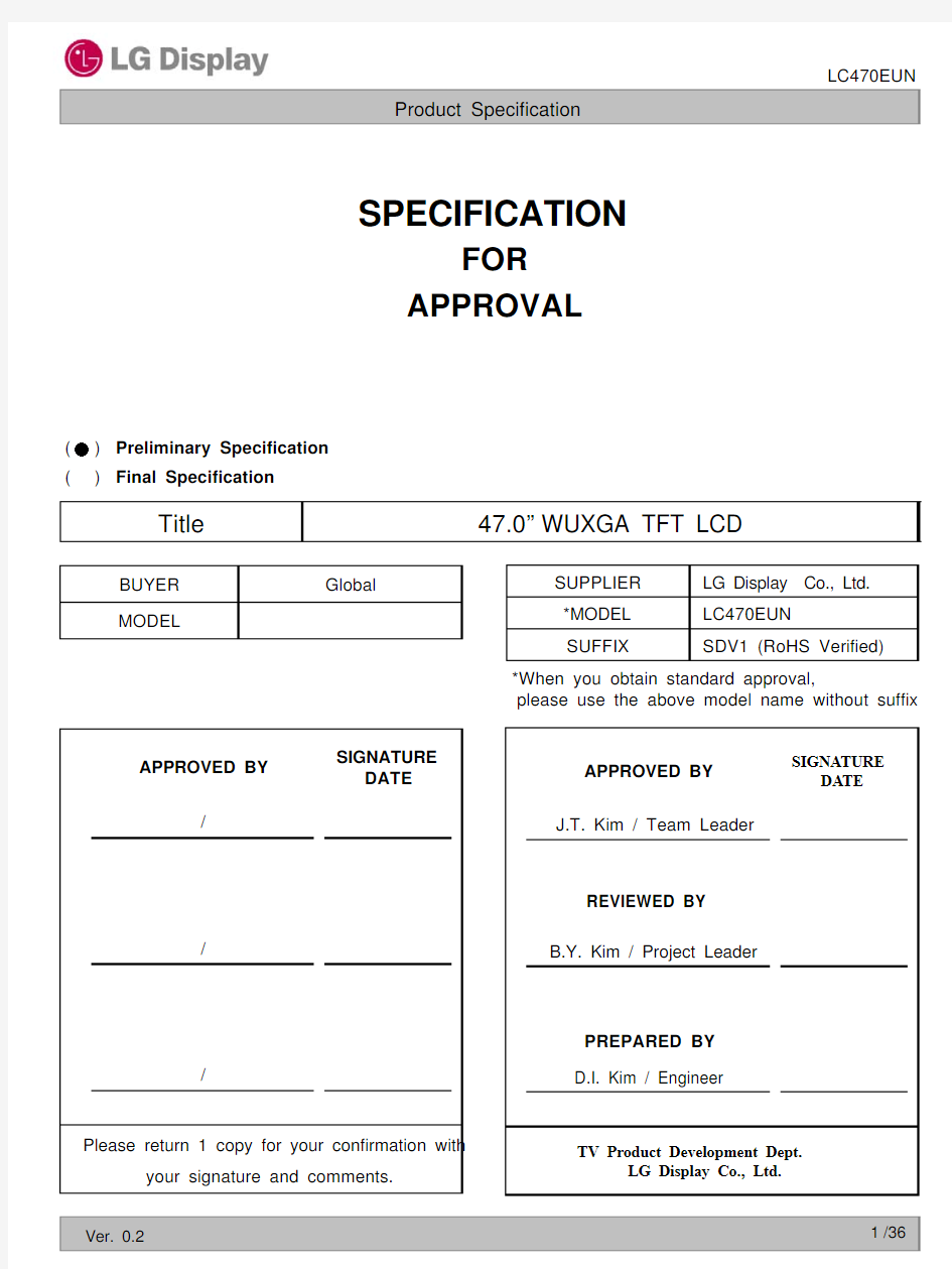
Title
47.0”WUXGA TFT LCD
BUYER Global
MODEL
SUPPLIER LG Display Co., Ltd.*MODEL LC470EUN
*When you obtain standard approval,
please use the above model name without suffix
SUFFIX
SDV1 (RoHS Verified)
SPECIFICATION
FOR APPROVAL
TV Product Development Dept.
D.I. Kim / Engineer
PREPARED BY
B.Y. Kim / Project Leader
REVIEWED BY
J.T. Kim / Team Leader
SIGNATURE
DATE
APPROVED BY Please return 1 copy for your confirmation with
/
/
/
SIGNATURE
DATE
APPROVED BY
))(
(Final Specification
Preliminary Specification ●
CONTENTS
Number
ITEM
Page
COVER 13-2INTERFACE CONNECTIONS 83-3SIGNAL TIMING SPECIFICATIONS 107-2EMC 25149
PRECAUTIONS
279-1MOUNTING PRECAUTIONS 279-2OPERATING PRECAUTIONS
279-3ELECTROSTATIC DISCHARGE CONTROL 289-4PRECAUTIONS FOR STRONG LIGHT EXPOSURE 289-5STORAGE
283-5COLOR DATA REFERENCE 7-3Environment 258
PACKING
268-1INFORMATION OF LCM LABEL 268-2PACKING FORM 26CONTENTS
2RECORD OF REVISIONS
31GENERAL DESCRIPTION 42ABSOLUTE MAXIMUM RATINGS 53
ELECTRICAL SPECIFICATIONS 63-1ELECTRICAL CHARACTERISTICS 63-4LVDS SIGNAL SPECIFICATIONS 113-6POWER SEQUENCE 154OPTICAL SPECIFICATIONS 175MECHANICAL CHARACTERISTICS 216RELIABILITY
247
INTERNATIONAL STANDARDS 257-1SAFETY 25
Revision No.
Revision Date
Page
Description
0.1Oct, 04, 2010-Preliminary Specification(First Draft)
0.2
Nov, 02, 2010
5Table 1. ABSOLUTE MAXIMUM RATINGS update
7Table 3. ELECTRICAL CHARACTERISTICS (Continue) update 8Table 4. MODULE CONNECTOR(CN1) PIN CONFIGURATION update
17Optical Specification update 22,23Mechanical Characteristics update 35
Appendix V update
9Table 5. LED DRIVER CONNECTOR PIN CONFIGURATION update
10Table 6. TIMING TABLE (DE Only Mode) update 15Power Sequence update 16Sequence for LED Driver update RECORD OF REVISIONS
1. General Description
The LC470EUN is a Color Active Matrix Liquid Crystal Display with an integral Light Emitting Diode (LED) backlight system. The matrix employs a-Si Thin Film Transistor as the active element. It is a transmissive display type which is operating in the normally black mode. It has a 46.96 inch diagonally measured active display area with WUXGA resolution (1080 vertical by 1920 horizontal pixel array). Each pixel is divided into Red, Green and Blue sub-pixels or dots which are arrayed in vertical stripes. Gray scale or the luminance of the sub-pixel color is determined with a 8-bit gray scale signal for each dot. Therefore, it can present a palette of more than 16.7Milion colors.
It has been designed to apply the 8-bit 2-port LVDS interface.
It is intended to support LCD TV, PCTV where high brightness, super wide viewing angle, high color gamut, high color depth and fast response time are important.
General Features
The following items are maximum values which, if exceeded, may cause faulty operation or permanent damage to the LCD module.
2. Absolute Maximum Ratings
Table 1. ABSOLUTE MAXIMUM RATINGS
1. Ambient temperature condition (Ta = 25 ±2 °C )
2. Temperature and relative humidity range are shown in the figure below. Wet bulb temperature should be Max 39°C, and no condensation of water.
3. Gravity mura can be guaranteed below 40°C condition.
4. The maximum operating temperatures is based on the test condition that the surface temperature
of display area is less than or equal to 68°C with LCD module alone in a temperature controlled chamber.Thermal management should be considered in final product design to prevent the surface temperature of display area from being over 68℃. The range of operating temperature may be degraded in case of improper thermal management in final product design.
90%
10
20
30
40
50
60
70
80
-200
10203040
50Wet Bulb
Temperature [°C ]
Storage
Operation
H u m i d i t y [(%)R H ]
10%
40%
60%
60
Note
3. Electrical Specifications 3-1. Electrical Characteristics
It requires two power inputs. One is employed to power for the LCD circuit. The other Is used for the LED backlight and LED Driver circuit.
1. The specified current and power consumption are under the V LCD =1
2.0V, Ta=25 ±2°C, f V =60Hz
condition whereas mosaic pattern(8 x 6) is displayed and f V is the frame frequency.2. The current is specified at the maximum current pattern.
3. The duration of rush current is about 2ms and rising time of power input is 0.5ms (min.).
Mosaic Pattern(8 x 6)
White : 255 Gray Black : 0 Gray
Note
Table 3. ELECTRICAL CHARACTERISTICS (Continue)
Notes :
1. Electrical characteristics are determined after the unit has been ‘ON’and stable for approximately 60
minutes at 25±2°C. The specified current and power consumption are under the typical supply Input voltage 24Vand V BR(Scan Duty: 100%), it is total power consumption.
2. The life time (MTTF) is determined as the time which luminance of the LED is 50% compared to that of initial
value at the typical LED current (Scan Duty :100%) on condition of continuous operating in LCM state at 25±2°C.
3. LGD recommend that the Scan Duty Freq. is synchronized with Two times harmonic of V_sync signal of
system. Though frequency is over 120Hz (max 252Hz), function of LED Driver is not affected.
4. The duration of rush current is about 200ms.
5. Even though inrush current is over the specified value, there is no problem if I2T spec of fuse is satisfied.
6. ExtV
BR-B signal have to input available duty range and sequence.
After Driver ON signal is applied, ExtV
BR-B should be sustained from 5% to 100% more than 500ms.
After that, ExtV
BR-B 1% and 100% is possible
For more information, please see 3-6-2. Sequence for LED Driver.
3-2. Interface Connections
This LCD module employs two kinds of interface connection, 51-pin connector is used for the module electronics and 14-pin connector is used for the integral backlight system.
3-2-1. LCD Module
-LCD Connector(CN1): FI-R51S-HF(manufactured by JAE) or compatible
Refer to below and next Page table
-Mating Connector : FI-R51HL(JAE) or compatible
Table 4. MODULE CONNECTOR(CN1) PIN CONFIGURATION
Note 1. All GND(ground) pins should be connected together to the LCD module’s metal frame.
2. All V LCD(power input) pins should be connected together.
3. All Input levels of LVDS signals are based on the EIA 644Standard.
4. #1~#6 & #9 NC (No Connection): These pins are used only for LGD (Do not connect)
5. Specific pins(pin No. #10) are used for OPC function of the LCD module.
If not used, these pins are no connection. (Please see the Appendix VI for more information.)
6. Specific pin No. #44is used for “No signal detection”of system signal interface.
It should be GND for NSB(No Signal Black) during the system interface signal is not.
If this pin is “H”, LCD Module displays AGP(Auto Generation Pattern).
3-2-2. Backlight Module
Table 5. LED DRIVER CONNECTOR PIN CONFIGURATION
◆Rear view of LCM
Master
-LED Driver Connector
: 20022WR -H14B1(Yeonho) or Equivalent -Mating Connector
: 20022HS -14B2or Equivalent
Pin No Symbol
Description
Note
1V BL Power Supply +24.0V 2V BL Power Supply +24.0V 3V BL Power Supply +24.0V 4V BL Power Supply +24.0V 5V BL Power Supply +24.0V 6GND Backlight Ground 7GND Backlight Ground 8GND Backlight Ground 9GND Backlight Ground 10GND Backlight Ground 1
11Status Back Light Status 212V ON/OFF Backlight ON/OFF control 3
13NC Don’t care 14
NC
Don’t care
Notes :1. GND should be connected to the LCD module’s metal frame.
2. Normal : Low (under 0.7V) / Abnormal : High (upper
3.0V) 3. The impedance of pin #12 is over 50 [K ?].
3-3. Signal Timing Specifications
Table 6 shows the signal timing required at the input of the LVDS transmitter. All of the interface signal timings should be satisfied with the following specification for normal operation.
Table 6. TIMING TABLE (DE Only Mode)
Note:1. The input of HSYNC & VSYNC signal does not have an effect on normal operation (DE Only Mode).
If you use spread spectrum of EMI, add some additional clock to minimum value for clock margin.
2. The performance of the electro-optical characteristics may be influenced by variance of the vertical
refresh rate and the horizontal frequency
※Timing should be set based on clock frequency.
3-4. LVDS Signal Specification
3-4-1. LVDS Input Signal Timing Diagram
0.7VDD
0.3VDD
DE(Data DCLK
DE, Data
3-4-2. LVDS Input Signal Characteristics
1) DC Specification
2) AC Specification
1. All Input levels of LVDS signals are based on the EIA 644 Standard. Note
V+ data
V-
V+ clk
V-clk
3-5. Color Data Reference
The brightness of each primary color(red,green,blue) is based on the 8bit gray scale data input for the color. The higher binary input, the brighter the color. Table 7 provides a reference for color versus data input. Table 7. COLOR DATA REFERENCE
3-6. Power Sequence
3-6-1. LCD Driving circuit
Table 8. POWER SEQUENCE
Interface Signal (Tx_clock)
Power for LED
Power Supply For LCD
V LCD
User Control Signal
(LVDS_select, OPC Enable)Note :
1. Even though T1 is over the specified value, there is no problem if I2T spec of fuse is satisfied.
2. If T2 is satisfied with specification after removing LVDS Cable, there is no problem.
3. The T3 / T4is recommended value, the case when failed to meet a minimum specification, abnormal display would be shown. There is no reliability problem.
4. T5 should be measured after the Module has been fully discharged between power off and on period.
5. If the on time of signals (Interface signal and user control signals) precedes the on time of Power (V LCD ),it will be happened abnormal display. When T6is NC status,T6 doesn’t need to be measured.
6. If there is no abnormal display, no problem.
3-6-2. Sequence for LED Driver
Power Supply For LED Driver
V ON/OFF
V BL
0V
Table 9. Power Sequence for LED Driver
Scan [PWM1~5]
3-6-3. Dip condition for LED Driver
V BL (Typ.) x 0.8
0 V
V BL : 24V
Values
Parameter
T5--10ms V BL (Typ) x 0.8
T6
500
--ms
2Min Typ Max Units Remarks
T120--ms 1
T2500--ms T310--ms T40--ms Notes : 1. T1 describes rising time of 0V to 24V and this parameter does not applied at restarting time.
Even though T1 is over the specified value, there is no problem if I 2T spec of fuse is satisfied.
Pritchard 880 or
equivalent
FIG. 1 Optical Characteristic Measurement Equipment and Method
4. Optical Specification
Optical characteristics are determined after the unit has been ‘ON’and stable in a dark environment at 25±2°C. The values are specified at 50cm from the LCD surface at a viewing angle of Φand θequal to 0 °.
FIG. 1 shows additional information concerning the measurement equipment and method.
Table 10. OPTICAL CHARACTERISTICS
Ta= 25±2°C, V LCD=12.0V, f V=60Hz, Dclk=74.25MHz,
EXTV BR-B=100%
Note : 1. Contrast Ratio(CR) is defined mathematically as :
Surface Luminance with all white pixels
Contrast Ratio =
Surface Luminance with all black pixels
It is measured at center 1-point.
2. Surface luminance are determined after the unit has been ‘ON’and 1 Hour after lighting the
backlight in a dark environment at 25±2°C. Surface luminance is the luminance value at center 1-point across the LCD surface 50cm from the surface with all pixels displaying white.For more information see the FIG. 2.
3. The variation in surface luminance , δWHITE is defined as :
δWHITE(5P) = Maximum(L on1,L on2, L on3, L on4, L on5) / Minimum(L on1,L on2, L on3, L on4, L on5)Where L on1to L on5are the luminance with all pixels displaying white at 5 locations . For more information, see the FIG. 2.
4. Response time is the time required for the display to transit from any gray to white (Rise Time, Tr R ) and from any gray to black (Decay time, Tr D ). For additional information see the FIG. 3.※G to G BW Spec stands for average value of all measured points.Photo Detector : RD-80S / Field : 2 °
5. G to G σis Variation of Gray to Gray response time composing a picture
G to G (σ) =
6. Viewing angle is the angle at which the contrast ratio is greater than 10. The angles are
determined for the horizontal or x axis and the vertical or y axis with respect to the z axis which is normal to the LCD module surface. For more information, see the FIG. 4.
7. Gray scale specification
Gamma Value is approximately 2.2. For more information, see the Table 11.
Σ(Xi-u)2
N
Xi = Individual Data u = Data average N : The number of Data
√
Measuring point for surface luminance & measuring point for luminance variation.
FIG. 2 5 Points for Luminance Measure
A : H / 4 mm
B : V / 4 mm
@ H,V : Active Area
Response time is defined as the following figure and shall be measured by switching the input signal for “Gray(N)”and “Black or White”.
10090
100
Optical Response
N = 0(Black)~255(White)
FIG. 4 Viewing Angle
Dimension of viewing angle range
φ