NAU88L25_ProductBrief_Rev0-3
NAU88L25 Ultra-Low Power Audio CODEC for Headphone/Headsets Application With 123dB Class G Headphone Drive and Advanced Headset Features
Description
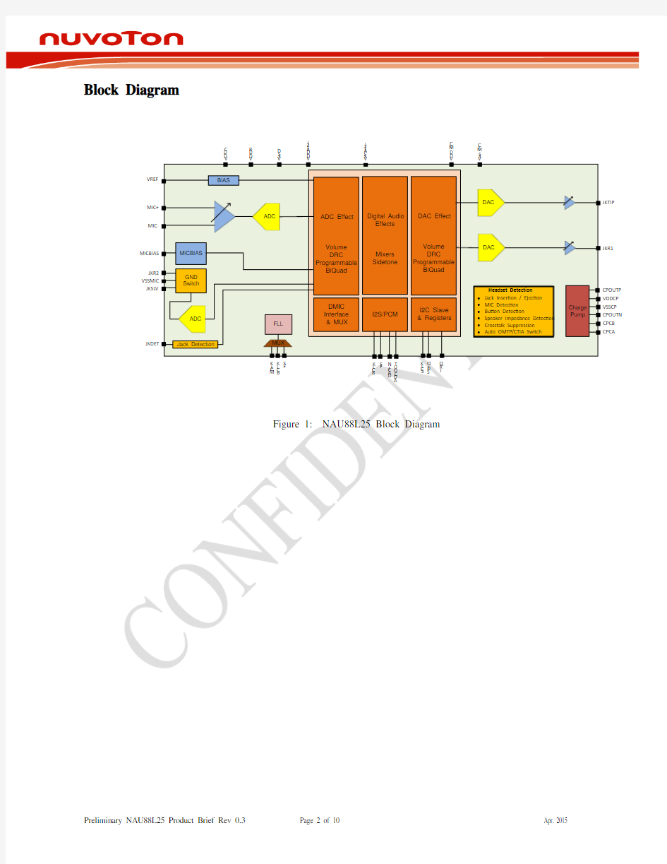
The NAU88L25 is an ultra-low power high performance audio codec designed for headphone or headset application in smartphone, tablet PC, Chromebook, laptop, game controller, bluetooth headphones and other portable devices. It includes one I2S/PCM interface, one high quality stereo DACs, one mono ADC, a Class G stereo heaphone amaplifier, and industry leading advanced headset features.
Advanced on-chip signal processing engine including dynamic range compressor (DRC), programmable bi-quad filters, sidetone and ditial mixers, can maximize audio qualiy enhencements and eliminate the undersirable frequency components. A frequency locked loop(FLL) is also integrated in the design to support various clocks wih less external components.
NAU88L25 has powerful headset detection mechanism, which detects jack insertion / ejection, microphone presence, speaker impedance, and up-to 8 user defined buttons with long/shory key press debouce circtuit. It also supports headphone crosstalk detection/suppression, and automatic microphone and ground swap feature to work automatically with both CTIA and OMTP headset format in a single chip.
The NAU88L25 operates with analog supply voltages from 1.6V to 1.8V, while the digital core can operate from 1.1V to 1.98V to conserve power. The NAU88L25 is specified for operation from -40°C to +85°C, and is available in QFN 32 or CSP package with 0.4mm pitch.
Key Features
?High Quality Audio CODEC
DAC : 123dB SNR & -85dB THD
ADC: 100dB SNR & -85dB THD
?High Performance Class G Output Driver Class G Headphone: 30mW (RL=32?, THD+N ≤ 1%)?MIC Inputs
One Differential or Two Single Ended
Input PGA: 0 to 36dB in 3dB Steps Programmable MIC Bias
?Digital Audio Interface:
I2S/PCM/TDM
?DSP
Sidetone & Digital Mixers
Dynamic Range Compressor (DRC) Programmable Bi-Quad Filters
?Power Consumption (Stereo, Quiescent) Class G Headphone – 4.5mW (RL=32?, fs=48KHz) ?Advanced Headset Features
Jack Insertion/Ejection
MIC Presence Detection
Speaker Impedance Detection
Up to 8 Button Detection with Short/Long Key Supports Headphone Crosstalk Detection / Suppression Automatic MIC / GND Swap (OMTP/CTIA Format)
?Package
QFN 32
CSP with 0.4mm Pitch (Optional)
?Application
PC (Laptop / UltraBook / Chromebook)
Game Controller
Tablets and Smartphones
Wearable Devices
Wireless Headphones / Headsets
Consumer Application
Block Diagram
V D D C
V D D B
V S S D
V D D A (2)
V S S A (2)
V D D M I C
V S S M I C CPCB
Pin Diagram
Pin Descriptions
Pin # Name Type Functionality
1 VDDA Supply Analog Supply
2 MICBIAS Analog Output Microphone Bias Output
3 VDDMIC Supply Microphone supply
4 VREF Analog I/O Internal DAC & ADC voltage reference decoupling I/O
5 VSSA Ground Analog Supply Ground
6 VDDA Supply Analog Supply
7 CPOUTP Analog I/O Charge Pump positive voltage
8 VSSCP Ground Charge Pump Supply ground
9 CPOUTN Analog I/O Charge Pump negative voltage
10 CPCB Analog I/O Charge Pump switching capacitor node B
11 CPCA Analog I/O Charge Pump switching capacitor node A
12 JKTIP (HPL) Analog Output Headphone left channel output
13 JKR1 (HPR)Analog Output Headphone right channel output
14 CPOUTN Analog I/O Charge Pump negative voltage
15 IRQ Digital Output Programmable Interrupt Output
16 GPIO1 Digital I/O General Purpose IO/I2C Address/SPI_CSB
17 SDIO Digital I/O Serial Data for I2C or SPI
18 SCLK Digital Input Serial Data Clock for I2C or SPI
19 MCLK Digital Input CODEC Master clock input
20 VDDB Supply Digital IO Supply
21 VSSD Ground Digital IO ground
22 VDDC Supply Digital core supply
23 FS Digital I/O Frame Sync input or output for I2S or PCM data
24 ADCOUT Digital Output Serial Audio data Output for I2S or PCM data
25 DACIN Digital Input Serial Audio data input for I2S or PCM data
26 BCLK Digital I/O Serial data bit clock input or output for I2S or PCM
data
27 JKDET Analog Input Jack detect input
28 JKSLV Analog I/O Headset Jack pin 4
29 VSSMIC Ground Analog Supply Ground
30 JKR2 Analog I/O Headset Jack pin 3
31 MIC+ Analog Input PGA MIC1+ Analog Input
32 MIC1- Analog Input PGA MIC1- Analog Input
Electrical Characteristics
Conditions: V DD A = V DD A = CV DD C = V DD B = 1.8V; V DD SPK = V DD MIC= 4.2V.
R L(Headphone) = 32 ?, f = 1k Hz, unless otherwise specified. Limits apply for T A = 25℃
Symbol Parameter Conditions Typical Limit Units (Limit)
I SD Shutdown Current Shutdown Mode
V DD A 0.2 1
μA V DD A 0.2 1
V DD B 0.2 1
CV DD C 2 10
V DD SPK 0.2 1
V DD MIC 0.2 1
I DD Headset Detection Standby Mode Standby Mode 300 μA Active Current(MP3 Mode)
f S = 44.1kHz, Stereo HP DAC On, HP On,
P OUT = 0mW. R L(HP) = 32? TBD mA
Headphone Amplifier
P O Output Power Stereo R L = 32?, DAC Inpu t, HPV VDD =
1.8V, f=1kHz, 22kHz BW, THD+N = 1%
(CSP package)
30 mW
Stereo R L = 32?, DAC Input, HPV VDD =
1.8V, f=1kHz, 22kHz BW, THD+N = 1%
(QFN package)
27 mW
Stereo R L = 16?, DAC Input, HPV VDD =
1.8V, f=1kHz, 22kHz BW, THD+N = 1%
(CSP Package)
35 mW
Stereo R L = 16?, DAC Input, HPV VDD =
1.8V, f=1kHz, 22kHz BW, THD+N = 1%
(QFN Package)
TBD mW
THD+N Total Harmonic Distortion + Noise R L = 32?, f=1kHz, P O = 20mW -85 dB
SNR Signal to Noise Ratio VOUT = 1VRMS, DAC Input, DAC_Gain
= 0dB, HP_Gain = 0dB, Digital Zero
Input, f=1kHz, A-Weighted, auto mute
disabled
113 dB
VOUT = 1VRMS, DAC Input, DAC_Gain
= 0dB, HP_Gain = 0dB, Digital Zero
Input, f=1kHz, A-Weighted, auto mute
enabled
123 dB
PSRR Power Supply Rejection Ratio f RIPPLE = 217Hz, V RIPPLE = 200mV P_P Input
Referred, HP_GAIN = 0dB
DAC Input, DAC_Gain = 0dB Ripple
Applied to V DD A& V DD A
90 dB
Mono_Gain = 0dB Ripple Applied to
V DD A& V DD A
90 dB
Stereo Single Ended Input Terminated,
Stereo_Gain = 0dB Ripple Applied to
V DD A& V DD A
90 dB
Symbol Parameter Conditions
Typical Limit
Units (Limit) X TALK Channel Crosstalk
Left Channel to Right Channel, -1dBFS, Gain = 0dB, f = 1kHz, MIC/GND Switching Off
100
dB
Left Channel to Right Channel, -1dBFS, Gain = 0dB, f = 1kHz, MIC/GND Switching On with HCS 70dB Internchannel Level Mismatch
+/- 0.1 dB Frequency Response F = 20Hz ~ 20KHz +/-0.005 dB Pop up Noise TBD
0.1 mV e OS Output Noise
DAC_Gain = 0dB, HP_Gain = 0dB,
f S =48kHz, OSR DAC = 128, A-Weighted 2.2
uV RMS Out of Band Noise Level
-60dB V OS
Output Offset Voltage
HP_Gain = 0dB, DAC_Gain = 0dB, DAC Input,
0.1
±0.5
mV
Power Consunption
No Load, No Signal, Amp on
f S = 48kHz, Stereo DAC On, Amp On, P OUT = 0mW. R L = 32? 4.5 mW
Fs Accuracy (44.1 / 48 KHz) +/- 0.02% Pop and Click Noise
0.1
mVpp
ADC
THD+N
ADC Total Harmonic Distortion + Noise
MIC Input, MIC_GAIN = 0dB, V IN =
1.0Vrms, f=1KHz, fs = 48KHz -90 dB MIC Input, MIC_GAIN = 30dB, Volume = 0dB, -60dBFS < ADC_Output < -12dBFS, Digital Gain = 0dB
-60
dB
SNR Signal to Noise Ratio
Reference = V OUT (0dBFS), A-Weighted, MIC Input, MIC Gain = 0dB,fs = 8KHz, Mono Differential Input
100 dB
Reference = V OUT (0dBFS), A-Weighted, MIC Input, MIC Gain = 6dB,fs = 8KHz, Mono Differential Input
98
dB
PSRR Power Supply Rejection Ratio V RIPPLE = 200mV P_P applied to V DD A , f RIPPLE = 217Hz, Input Referred, MIC_GAIN = 0dB Differential Input 90 dB CMRR Common Mode Rejection Ratio TBD 60
dB FS ADC ADC Full Scale Input Level V DD A = 1.8V 1 V RMS Minimum Input Impdeance
10 KOhm Frequency Response f = 20Hz ~ 20KHz +/-0.05 dB Pop up Noise TBD
0.1 mV
Power Consumption
No Load, No Signal, Amp on
fS = 44.1kHz, ADC On, Amp On, POUT = 0 mW. RL = 10K?
1.8
mW
Absolute Maximum Ratings
Parameter Min Max Units Digital Supply Range -0.3 2.2 V
Digital I/O Supply Range -0.3 6.0 V
Analog Supply Range -0.3 2.2 V Headphone Supply Range -0.3 2.2 V Microphone Bias Supply Voltage -0.3 6.0 V
Voltage Input Digital Range DGND - 0.3 VDD + 0.3 V
Voltage Input Analog Range AGND - 0.3 VDD + 0.3 V Junction Temperature, T J-40 +150 ℃
Storage Temperature -65 +150 ℃CAUTION: Do not operate at or near the maximum ratings listed for extended periods. Exposure to such conditions may adversely influence product reliability and result in failures not covered by warranty
Operating Conditions
Condition Symbol Min Typical Max Units Digital Supply Range VDDC 1.1 1.2 1.98 V Digital I/O Supply Range VDDB 1.6 1.8 3.6 V Analog Supply Range VDDA 1.6 1.8 2.0 V Headphone Supply Range VDDA 1.6 1.8 2.0 V Microphone Bias Supply Voltage VDDMIC 2.5 4.2 5.0 V Temperature Range T A-40 +85 ℃
Digital I/O
Parameter Symbol Comments/Conditions Min Max Uni ts
Input LOW level V IL VDDB = 1.8V 0.33 * VDDB
V VDDB = 3.3V 0.37*VDDB
Input HIGH level V IH VDDB = 1.8V 0.57*VDDB
V VDDB = 3.3V 0.63*VDDB
Output HIGH level V OH I Load = 1mA VDDB=1.8V 0.9 * VDDB
V VDDB = 3.3V 0.95*VDDB
Output LOW level V OL I Load = 1mA VDDB = 1.8V 0.1 * VDDB
V VDDB=3.3V 0.05*VDDB
Part Number Dimension Package Package Material
NAU88L25YG 5 x 5 mm QFN-32L Green Nuvoton Part Number Description
NAU88L25YG
Package Material:
G =Pb-free Package
Package Type:
Y = QFN Package
32-lead plastic QFN 32L; 5X5mm2, 0.8mm thickness, 0.5mm lead pitch
Version History
VERSION DATE PAGE DESCRIPTION
0.1 11/20/2014 NA Preliminary Version
0.2 03/10/2015 Updated the pin-out and pin-descriptions
0.3 04/10/2015 8 Ordering info is added.
Table 1: Version History
Important Notice
Nuvoton products are not designed, intended, authorized or warranted for use as components in systems or equipment intended for surgical implantation, atomic energy control instruments, airplane or spaceship instruments, transportation instruments, traffic signal instruments, combustion control instruments, or for other applications intended to support or sustain life. Furthermore, Nuvoton products are not intended for applications wherein failure of Nuvoton products could result or lead to a situation wherein personal injury, death or severe property or environmental damage could occur.
Nuvoton customers using or selling these products for use in such applications do so at their own risk and agree to fully indemnify Nuvoton for any damages resulting from such improper use or sales.