SMAJ188CA中文资料
SMAJ5.0 thru SMAJ188CA
Vishay General Semiconductor
Document Number: 88390For technical questions within your region, please contact one of the following:https://www.360docs.net/doc/789890757.html,
Surface Mount T RANS Z ORB ? Transient Voltage Suppressors
FEATURES
?Low profile package
?Ideal for automated placement ?Glass passivated chip junction
?
?cycle): 0.01 % (300 W above 78 V) ?Excellent clamping capability ?Very fast response time
?Low incremental surge resistance
?Meets MSL level 1, per J-STD-020, LF maximum peak of 260 °C
?Solder dip 260 °C, 40 s ?Component in accordance to RoHS 2002/95/EC and WEEE 2002/96/EC TYPICAL APPLICATIONS
Use in sensitive electronics protection against voltage transients induced by inductive load switching and lighting on ICs, MOSFET, signal lines of sensor units for consumer, computer, industrial, automotive and telecommunication.
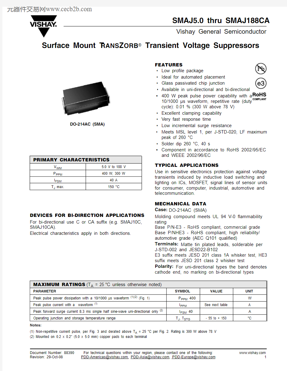
MECHANICAL DATA Case: DO-214AC (SMA)
Molding compound meets UL 94 V-0 flammability rating
Base P/N-E3 - RoHS compliant, commercial grade Base P/NHE3 - RoHS compliant, high reliability/automotive grade (AEC Q101 qualified)
Terminals: Matte tin plated leads, solderable per J-STD-002 and JESD22-B102
E3 suffix meets JESD 201 class 1A whisker test, HE3suffix meets JESD 201 class 2 whisker test
Polarity: For uni-directional types the band denotes cathode end, no marking on bi-directional types
DEVICES FOR BI-DIRECTION APPLICATIONS For bi-directional use C or CA suffix (e.g. SMAJ10C,SMAJ10CA).
Electrical characteristics apply in both directions.
PRIMARY CHARACTERISTICS
V WM 5.0 V to 188 V P PPM 400 W, 300 W
I FSM 40 A T J max.
150 °C
DO-214AC (SMA)
Notes:
(1) Non-repetitive current pulse, per Fig. 3 and derated above T A = 25 °C per Fig. 2. Rating is 300 W above 78 V (2) Mounted on 0.2 x 0.2" (5.0 x 5.0 mm) copper pads to each terminal
MAXIMUM RATINGS (T A = 25°C unless otherwise noted)
PARAMETER
SYMBOL VALUE UNIT Peak pulse power dissipation with a 10/1000 μs waveform (1)(2) (Fig. 1) P PPM 400 W Peak pulse current with a waveform (1)
I PPM See next table A Peak forward surge current 8.3 ms single half sine-wave uni-directional only (2) I FSM 40 A
Operating junction and storage temperature range T J , T STG
- 55 to + 150
°C
元器件交易网https://www.360docs.net/doc/789890757.html,
SMAJ5.0 thru SMAJ188CA
Vishay General Semiconductor
https://www.360docs.net/doc/789890757.html, For technical questions within your region, please contact one of the following:Document Number: 88390
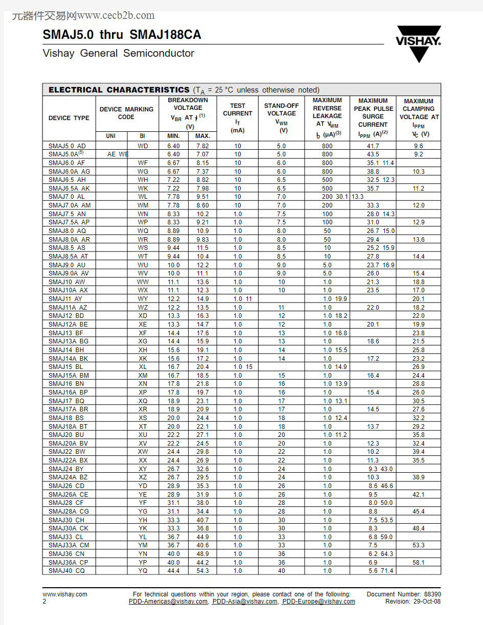
ELECTRICAL CHARACTERISTICS (T A = 25°C unless otherwise noted)
DEVICE TYPE
DEVICE MARKING
CODE BREAKDOWN VOLTAGE V BR AT I T (1)
(V) TEST CURRENT
I T (mA)
STAND-OFF VOLTAGE V WM (V)
MAXIMUM REVERSE LEAKAGE AT V WM I D (μA) (3)
MAXIMUM PEAK PULSE SURGE CURRENT I PPM (A)
(2)MAXIMUM CLAMPING VOLTAGE AT I PPM
V C (V)UNI
BI
MIN.
MAX.
SMAJ5.0 AD WD 6.40 7.82 10 5.0 800 41.7 9.6
SMAJ5.0A
(5)
AE WE 6.40 7.07 10 5.0 800 43.5 9.2 SMAJ6.0 AF WF 6.67 8.15 10 6.0 800 35.1 11.4 SMAJ6.0A AG WG 6.67 7.37 10 6.0 800 38.8 10.3 SMAJ6.5 AH WH 7.22 8.82 10 6.5 500 32.5 12.3 SMAJ6.5A AK WK 7.22 7.98 10 6.5 500 35.7 11.2 SMAJ7.0 AL WL 7.78 9.51 10 7.0 200 30.1 13.3 SMAJ7.0A AM WM 7.78 8.60 10 7.0 200 33.3 12.0 SMAJ7.5 AN WN 8.33 10.2 1.0 7.5 100 28.0 14.3 SMAJ7.5A AP WP 8.33 9.21 1.0 7.5 100 31.0 12.9 SMAJ8.0 AQ WQ 8.89 10.9 1.0 8.0 50 26.7 15.0 SMAJ8.0A AR WR 8.89 9.83 1.0 8.0 50 29.4 13.6 SMAJ8.5 AS WS 9.44 11.5 1.0 8.5 10 25.2 15.9 SMAJ8.5A AT WT 9.44 10.4 1.0 8.5 10 27.8 14.4 SMAJ9.0 AU WU 10.0 12.2 1.0 9.0 5.0 23.7 16.9 SMAJ9.0A AV WV 10.0 11.1 1.0 9.0 5.0 26.0 15.4 SMAJ10 AW WW 11.1 13.6 1.0 10 1.0 21.3 18.8 SMAJ10A AX WX 11.1 12.3 1.0 10 1.0 23.5 17.0 SMAJ11 AY WY 12.2 14.9 1.0 11 1.0 19.9 20.1 SMAJ11A AZ WZ 12.2 13.5 1.0 11 1.0 22.0 18.2 SMAJ12 BD XD 13.3 16.3 1.0 12 1.0 18.2 22.0 SMAJ12A BE XE 13.3 14.7 1.0 12 1.0 20.1 19.9 SMAJ13 BF XF 14.4 17.6 1.0 13 1.0 16.8 23.8 SMAJ13A BG XG 14.4 15.9 1.0 13 1.0 18.6 21.5 SMAJ14 BH XH 15.6 19.1 1.0 14 1.0 15.5 25.8 SMAJ14A BK XK 15.6 17.2 1.0 14 1.0 17.2 23.2 SMAJ15 BL XL 16.7 20.4 1.0 15 1.0 14.9 26.9 SMAJ15A BM XM 16.7 18.5 1.0 15 1.0 16.4 24.4 SMAJ16 BN XN 17.8 21.8 1.0 16 1.0 13.9 28.8 SMAJ16A BP XP 17.8 19.7 1.0 16 1.0 15.4 26.0 SMAJ17 BQ XQ 18.9 23.1 1.0 17 1.0 13.1 30.5 SMAJ17A BR XR 18.9 20.9 1.0 17 1.0 14.5 27.6 SMAJ18 BS XS 20.0 24.4 1.0 18 1.0 12.4 32.2 SMAJ18A BT XT 20.0 22.1 1.0 18 1.0 13.7 29.2 SMAJ20 BU XU 22.2 27.1 1.0 20 1.0 11.2 35.8 SMAJ20A BV XV 22.2 24.5 1.0 20 1.0 12.3 32.4 SMAJ22 BW XW 24.4 29.8 1.0 22 1.0 10.2 39.4 SMAJ22A BX XX 24.4 26.9 1.0 22 1.0 11.3 35.5 SMAJ24 BY XY 26.7 32.6 1.0 24 1.0 9.3 43.0 SMAJ24A BZ XZ 26.7 29.5 1.0 24 1.0 10.3 38.9 SMAJ26 CD YD 28.9 35.3 1.0 26 1.0 8.6 46.6 SMAJ26A CE YE 28.9 31.9 1.0 26 1.0 9.5 42.1 SMAJ28 CF YF 31.1 38.0 1.0 28 1.0 8.0 50.0 SMAJ28A CG YG 31.1 34.4 1.0 28 1.0 8.8 45.4 SMAJ30 CH YH 33.3 40.7 1.0 30 1.0 7.5 53.5 SMAJ30A CK YK 33.3 36.8 1.0 30 1.0 8.3 48.4 SMAJ33 CL YL 36.7 44.9 1.0 33 1.0 6.8 59.0 SMAJ33A CM YM 36.7 40.6 1.0 33 1.0 7.5 53.3 SMAJ36 CN YN 40.0 48.9 1.0 36 1.0 6.2 64.3 SMAJ36A CP YP 40.0 44.2 1.0 36 1.0 6.9 58.1 SMAJ40 CQ YQ 44.4 54.3 1.0 40 1.0 5.6 71.4
元器件交易网https://www.360docs.net/doc/789890757.html,
SMAJ5.0 thru SMAJ188CA
Vishay General Semiconductor
Document Number: 88390For technical questions within your region, please contact one of the following:https://www.360docs.net/doc/789890757.html,
Notes:
(1) Pulse test: t p ≤ 50 ms
(2) Surge current waveform per Fig. 3 and derate per Fig. 2
(3) For bi-directional types having V WM of 10 V and less, the I D limit is doubled (4) All terms and symbols are consistent with ANSI/IEEE C62.35(5) For the bi-directional SMAJ5.0CA, the maximum V BR is 7.25 V (6) V F = 3.5 V at I F = 25 A (uni-directional only)
SMAJ40A CR YR 44.4 49.1 1.0 40
1.0 6.2 64.5
SMAJ43 CS YS 47.8 58.4 1.0 43 1.0 5.2 76.7 SMAJ43A CT YT 47.8 52.8 1.0 43 1.0 5.8 69.4 SMAJ45 CU YU 50.0 61.1 1.0 45 1.0 5.0 80.3 SMAJ45A CV YV 50.0 55.3 1.0 45 1.0 5.5 72.7 SMAJ48 CW YW 53.3 65.1 1.0 48 1.0 4.7 85.5 SMAJ48A CX YX 53.3 58.9 1.0 48 1.0 5.2 77.4 SMAJ51 CY YY 56.7 69.3 1.0 51 1.0 4.4 91.1 SMAJ51A CZ YZ 56.7 62.7 1.0 51 1.0 4.9 82.4 SMAJ54 RD ZD 60.0 73.3 1.0 54 1.0 4.2 96.3 SMAJ54A RE ZE 60.0 66.3 1.0 54 1.0 4.6 87.1 SMAJ58 RF ZF 64.4 78.7 1.0 58 1.0 3.9 103 SMAJ58A RG ZG 64.4 71.2 1.0 58 1.0 4.3 93.6 SMAJ60 RH ZH 66.7 81.5 1.0 60 1.0 3.7 107 SMAJ60A RK ZK 66.7 73.7 1.0 60 1.0 4.1 96.8 SMAJ64 RL ZL 71.1 86.9 1.0 64 1.0 3.5 114 SMAJ64A RM ZM 71.1 78.6 1.0 64 1.0 3.9 103 SMAJ70 RN ZN 77.8 95.1 1.0 70 1.0 3.2 125 SMAJ70A RP ZP 77.8 86.0 1.0 70 1.0 3.5 113 SMAJ75 RQ ZQ 83.3 102 1.0 75 1.0 3.0 134 SMAJ75A RR ZR 83.3 92.1 1.0 75 1.0 3.3 121 SMAJ78 RS ZS 86.7 106 1.0 78 1.0 2.9 139 SMAJ78A RT ZT 86.7 95.8 1.0 78 1.0 3.2 126 SMAJ85 RU ZU 94.4 115 1.0 85 1.0 2.0 151 SMAJ85A RV ZV 94.4 104 1.0 85 1.0 2.2 137 SMAJ90 RW ZW 100 122 1.0 90 1.0 1.9 160 SMAJ90A RX ZX 100 111 1.0 90 1.0 2.1 146 SMAJ100 RY ZY 111 136 1.0 100 1.0 1.7 179 SMAJ100A RZ ZZ 111 123 1.0 100 1.0 1.9 162 SMAJ110 VD VD 122 149 1.0 110 1.0 1.5 196 SMAJ110A SE VE 122 135 1.0 110 1.0 1.7 177 SMAJ120 SF VF 133 163 1.0 120 1.0 1.4 214 SMAJ120A VG VG 133 147 1.0 120 1.0 1.6 193 SMAJ130 SH VH 144 176 1.0 130 1.0 1.3 231 SMAJ130A VK VK 144 159 1.0 130 1.0 1.4 209 SMAJ150 SL VL 167 204 1.0 150 1.0 1.1 268 SMAJ150A VM VM 167 185 1.0 150 1.0 1.2 243 SMAJ160 SN VN 178 218 1.0 160 1.0 1.0 287 SMAJ160A SP VP 178 197 1.0 160 1.0 1.2 259 SMAJ170 SQ VQ 189 231 1.0 170 1.0 0.99 304 SMAJ170A SR VR 189 209 1.0 170 1.0 1.09 275 SMAJ188 ST VT 209 255 1.0 188 1.0 0.90 344 SMAJ188A SS VS 209 231 1.0 188 1.0 0.91 328
ELECTRICAL CHARACTERISTICS (T A = 25°C unless otherwise noted)
DEVICE TYPE
DEVICE MARKING
CODE BREAKDOWN VOLTAGE V BR AT I T (1)
(V) TEST CURRENT
I T (mA)
STAND-OFF VOLTAGE V WM (V)
MAXIMUM REVERSE LEAKAGE AT V WM I D (μA) (3)
MAXIMUM PEAK PULSE SURGE CURRENT I PPM (A) (2)
MAXIMUM CLAMPING VOLTAGE AT I PPM
V C (V)UNI
BI
MIN.
MAX.
元器件交易网https://www.360docs.net/doc/789890757.html,
SMAJ5.0 thru SMAJ188CA
Vishay General Semiconductor
https://www.360docs.net/doc/789890757.html, For technical questions within your region, please contact one of the following:Document Number: 88390
Note:
(1) Mounted on minimum recommended pad layout
Note:
(1) Automotive grade AEC Q101 qualified
RATINGS AND CHARACTERISTICS CURVES (T A = 25 °C unless otherwise noted)
THERMAL CHARACTERISTICS (T A = 25°C unless otherwise noted)
PARAMETER
SYMBOL VALUE UNIT Typical thermal resistance, junction to ambient (1) R θJA 120 °C/W
Typical thermal resistance, junction to lead R θJL
30
°C/W
ORDERING INFORMATION (Example)
PREFERRED P/N UNIT WEIGHT (g)
PREFERRED PACKAGE CODE
BASE QUANTITY
DELIVERY MODE
SMAJ5.0A-E3/610.0646118007" diameter plastic tape and reel SMAJ5.0A-E3/5A 0.0645A 750013" diameter plastic tape and reel SMAJ5.0AHE3/61 (1)0.0646118007" diameter plastic tape and reel SMAJ5.0AHE3/5A (1)
0.064
5A
7500
13" diameter plastic tape and reel
Figure 1. Peak Pulse Power Rating Curve Figure 2. Pulse Power or Current vs. Initial Junction Temperature
Figure 3. Pulse Waveform
Figure 4. Typical Junction Capacitance
元器件交易网https://www.360docs.net/doc/789890757.html,
SMAJ5.0 thru SMAJ188CA
Vishay General Semiconductor
Document Number: 88390For technical questions within your region, please contact one of the following:https://www.360docs.net/doc/789890757.html,
PACKAGE OUTLINE DIMENSIONS in inches (millimeters)
Figure 5. Typical Transient Thermal Impedance
Figure 6. Maximum Non-Repetitive Forward Surge Current
Uni-Directional Only
元器件交易网https://www.360docs.net/doc/789890757.html,
Disclaimer Legal Disclaimer Notice
Vishay
All product specifications and data are subject to change without notice.
Vishay Intertechnology, Inc., its affiliates, agents, and employees, and all persons acting on its or their behalf (collectively, “Vishay”), disclaim any and all liability for any errors, inaccuracies or incompleteness contained herein or in any other disclosure relating to any product.
Vishay disclaims any and all liability arising out of the use or application of any product described herein or of any information provided herein to the maximum extent permitted by law. The product specifications do not expand or otherwise modify Vishay’s terms and conditions of purchase, including but not limited to the warranty expressed therein, which apply to these products.
No license, express or implied, by estoppel or otherwise, to any intellectual property rights is granted by this document or by any conduct of Vishay.
The products shown herein are not designed for use in medical, life-saving, or life-sustaining applications unless otherwise expressly indicated. Customers using or selling Vishay products not expressly indicated for use in such applications do so entirely at their own risk and agree to fully indemnify Vishay for any damages arising or resulting from such use or sale. Please contact authorized Vishay personnel to obtain written terms and conditions regarding products designed for such applications.
Product names and markings noted herein may be trademarks of their respective owners.
元器件交易网https://www.360docs.net/doc/789890757.html,
Document Number: https://www.360docs.net/doc/789890757.html,