Emerging Photoluminescence in Monolayer MoS2
Emerging Photoluminescence in Monolayer MoS 2
Andrea Splendiani,?,?Liang Sun,?Yuanbo Zhang,?Tianshu Li,§Jonghwan Kim,?Chi-Yung Chim,?Giulia Galli,§and Feng Wang*,?,|
?
Physics Department,University of California at Berkeley,Berkeley,California 94720,?Scuola Galileiana di Studi Superiori di Padova,35122Padova,Italy,§Chemistry Department,University of California at Davis,Davis,
California 95616,and |Materials Science Division,Lawrence Berkeley National Laboratory,Berkeley,California 94720
ABSTRACT Novel physical phenomena can emerge in low-dimensional nanomaterials.Bulk MoS 2,a prototypical metal dichalcogenide,is an indirect bandgap semiconductor with negligible photoluminescence.When the MoS 2crystal is thinned to monolayer,however,a strong photoluminescence emerges,indicating an indirect to direct bandgap transition in this d-electron system.This observation shows that quantum con?nement in layered d-electron materials like MoS 2provides new opportunities for engineering the electronic structure of matter at the nanoscale.
KEYWORDS Photoluminescence,two-dimensional materials,metal dichalcogenide
R
ecent advances in fabrication of ultrathin layered materials down to unit cell thickness (monolayers)1have enabled explorations of new low-dimensional
physics,as exempli?ed by massless Dirac fermions and anomalous quantum Hall effects observed in monolayer graphene.2,3Layered transition metal dichalcogenides rep-resent another class of materials,in which d-electrons’interactions can give rise to new physical phenomena.4,5MoS 2is a prototypical transition metal chalcogenide materi-al.It is composed of covalently bonded S -Mo -S sheets that are bound by weak van der Waals forces.In its bulk form,MoS 2is a semiconductor with an indirect bandgap of about 1eV 6,7and it has been exploited for photovoltaic 6and photocatalytic 7applications due to its strong absorption in the solar spectrum region.Quantum con?nement effects on the electronic structure and optical properties of MoS 2have been previously observed in MoS 2thin ?lms 8,9as well as in MoS 2nanoplates 10and nanotubes.11However,little is known about the properties of extended two-dimensional MoS 2sheets down to unit cell thickness.
Here we report the emergence of photoluminescence in ultrathin layers of MoS 2.We found that MoS 2photolumines-cence,surprisingly,increases with decreasing layer thick-ness,and that luminescence from a monolayer is the strongest while it is absent in bulk material.This unusual luminescence behavior is in accord with a recent theoretical prediction;MoS 2,an indirect bandgap material in its bulk form,becomes a direct bandgap semiconductor when thinned to a monolayer.Our results demonstrate that quantum con?nement in layered d-electron materials have
manifestations drastically different from those found in sp-bonded semiconductor nanostructures.
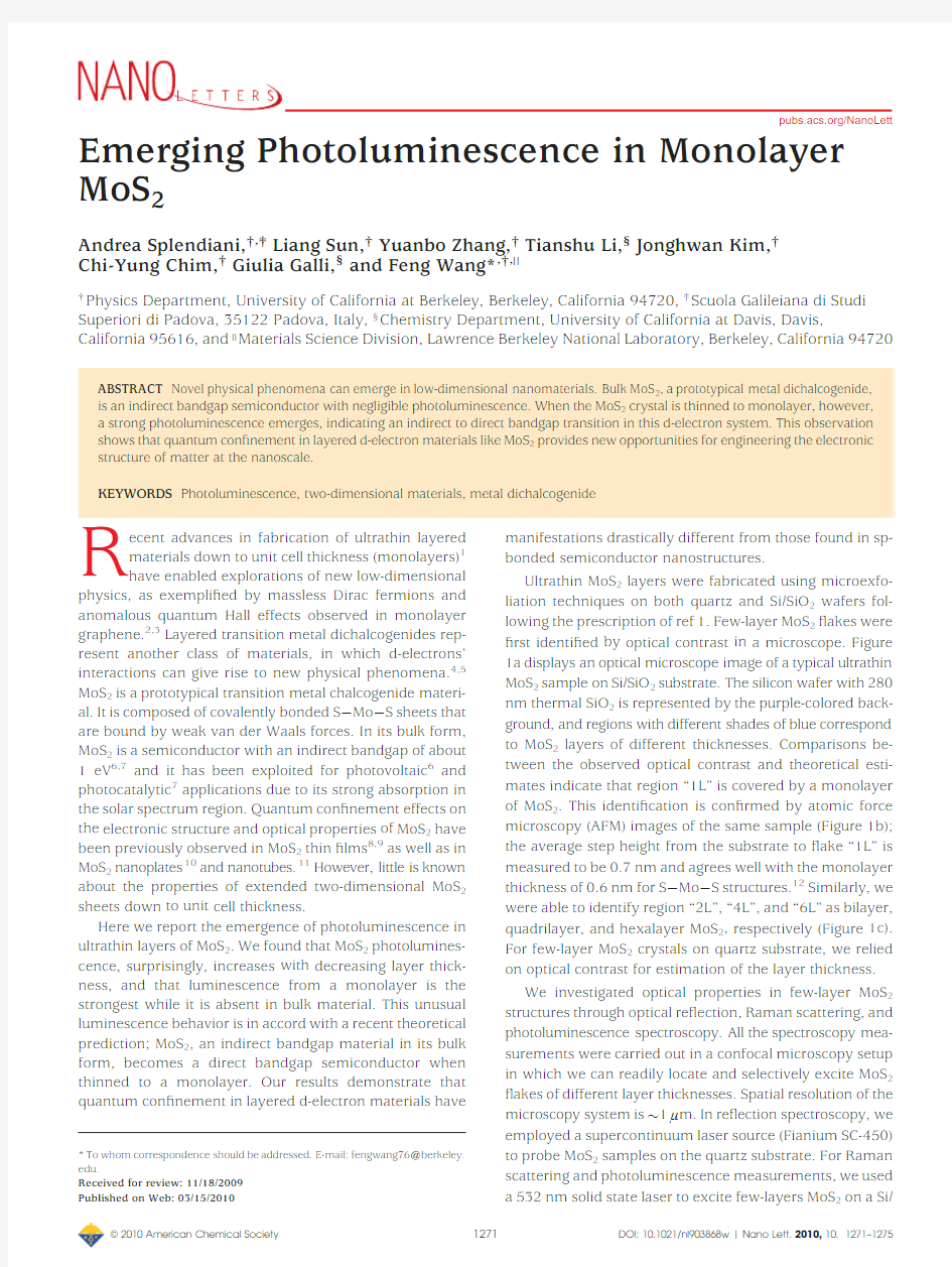
Ultrathin MoS 2layers were fabricated using microexfo-liation techniques on both quartz and Si/SiO 2wafers fol-lowing the prescription of ref 1.Few-layer MoS 2?akes were ?rst identi?ed by optical contrast in a microscope.Figure 1a displays an optical microscope image of a typical ultrathin MoS 2sample on Si/SiO 2substrate.The silicon wafer with 280nm thermal SiO 2is represented by the purple-colored back-ground,and regions with different shades of blue correspond to MoS 2layers of different https://www.360docs.net/doc/7d16774813.html,parisons be-tween the observed optical contrast and theoretical esti-mates indicate that region “1L”is covered by a monolayer of MoS 2.This identi?cation is con?rmed by atomic force microscopy (AFM)images of the same sample (Figure 1b);the average step height from the substrate to ?ake “1L”is measured to be 0.7nm and agrees well with the monolayer thickness of 0.6nm for S -Mo -S structures.12Similarly,we were able to identify region “2L”,“4L”,and “6L”as bilayer,quadrilayer,and hexalayer MoS 2,respectively (Figure 1c).For few-layer MoS 2crystals on quartz substrate,we relied on optical contrast for estimation of the layer thickness.We investigated optical properties in few-layer MoS 2structures through optical re?ection,Raman scattering,and photoluminescence spectroscopy.All the spectroscopy mea-surements were carried out in a confocal microscopy setup in which we can readily locate and selectively excite MoS 2?akes of different layer thicknesses.Spatial resolution of the microscopy system is ~1μm.In re?ection spectroscopy,we employed a supercontinuum laser source (Fianium SC-450)to probe MoS 2samples on the quartz substrate.For Raman scattering and photoluminescence measurements,we used a 532nm solid state laser to excite few-layers MoS 2on a Si/
*To whom correspondence should be addressed.E-mail:fengwang76@https://www.360docs.net/doc/7d16774813.html,.
Received for review:11/18/2009Published on Web:
03/15/2010
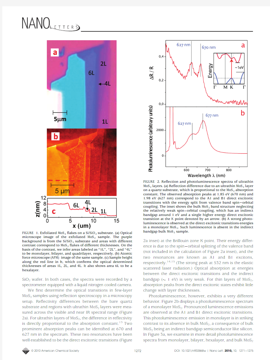
SiO 2wafer.In both cases,the spectra were recorded by a spectrometer equipped with a liquid nitrogen cooled camera.We ?rst determine the optical transitions in few-layer MoS 2samples using re?ection spectroscopy in a microscopy setup.Re?ectivity differences between the bare quartz substrate and regions with ultrathin MoS 2layers were mea-sured across the visible and near IR spectral range (Figure 2a).For ultrathin layers of MoS 2,the difference in re?ectivity is directly proportional to the absorption constant.13Two prominent absorption peaks can be identi?ed at 670and 627nm in the spectrum.These two resonances have been well established to be the direct excitonic transitions (Figure
2a inset)at the Brillouin zone K point.Their energy differ-ence is due to the spin -orbital splitting of the valence band (not included in the calculation of Figure 2a inset),and the two resonances are known as A1and B1excitons,respectively.14,15(The strong peak at 532nm is the elastic scattered laser radiation.)Optical absorption at energies between the direct excitonic transitions and the indirect bandgap (~1eV)is very weak.For thin layers of MoS 2,absorption peaks from the direct excitonic states exhibit little change with layer thicknesses.
Photoluminescence,however,exhibits a very different behavior.Figure 2b displays a photoluminescence spectrum of a monolayer MoS 2.Pronounced luminescence emissions are observed at the A1and B1direct excitonic transitions.This photoluminescence emission in monolayer is in striking contrast to its absence in bulk MoS 2,a consequence of bulk MoS 2being an indirect bandgap semiconductor like silicon.In Figure 3a,we examine in more detail photoluminescence spectra from monolayer,bilayer,hexalayer,and bulk MoS
2
FIGURE 1.Exfoliated MoS 2?akes on a Si/SiO 2substrate.(a)Optical microscope image of the exfoliated MoS 2sample.The purple background is from the Si/SiO 2substrate and areas with different contrast correspond to MoS 2?akes of different thicknesses.On the basis of the contrast,we infer areas labeled as “1L”,“2L”,and “4L”to be monolayer,bilayer,and quadrilayer,respectively.(b)Atomic force microscope (AFM)image of the same sample.(c)Sample height along the red line in b,which con?rms the optical determined thicknesses of areas 1L,2L,and 4L.It also shows area 6L to be a
hexalayer.
FIGURE 2.Re?ection and photoluminescence spectra of ultrathin MoS 2layers.(a)Re?ection difference due to an ultrathin MoS 2layer on a quartz substrate,which is proportional to the MoS 2absorption constant.The observed absorption peaks at 1.85eV (670nm)and 1.98eV (627nm)correspond to the A1and B1direct excitonic transitions with the energy split from valence band spin -orbital coupling.The inset shows the bulk MoS 2band structure neglecting the relatively weak spin -orbital coupling,which has an indirect bandgap around 1eV and a single higher energy direct excitonic transition at the K point denoted by an arrow.(b)A strong photo-luminescence is observed at the direct excitonic transitions energies in a monolayer MoS 2.Such luminescence is absent in the indirect bandgap bulk MoS 2
sample.
(in the form of very thick ?akes).In addition to the relatively broad photoluminescence,three prominent Raman modes can be identi?ed in the spectra:the ?rst peak corresponds to a MoS 2Raman excitation with a 408cm -1Raman shift 12and the next two at 520and 1030cm -1are the ?rst and second order Raman peaks from the silicon substrate.16In bulk MoS 2,no photoluminescence is observable and the MoS 2Raman signal is weak because of the local ?eld effect,that is,the local electric ?eld at a high refractive index material like MoS 2is much weaker than the incident electri-cal ?eld.For ultrathin MoS 2layers where local ?eld effects are relatively small,the Raman and photoluminescence intensities show opposite layer dependence:MoS 2Raman signal is the weakest in the monolayer MoS 2(due to reduced amount of material),while photoluminescence is the stron-gest in spite of the reduced amount of material.This surpris-ing behavior of the photoluminescence indicates that lumi-nescence quantum ef?ciency is much higher in MoS 2monolayer than in multilayer and in the bulk.
Next we determine layer dependent luminescence quan-tum ef?ciency ηLum using an internal calibrator provided by MoS 2Raman signal.MoS 2Raman intensity I Raman and lumi-nescence intensity I Lum are affected in the same manner by effects such as laser excitation intensity,quantity of material,and local electric ?eld factors;therefore such external effects are canceled out in the ratio I Lum /I Raman and this ratio provides a measure of intrinsic luminescence quantum ef?ciency through the quantity ηLum ≈ηRaman (I Lum /I Raman ).In this equa-tion,we have neglected the small energy difference between luminescence and Raman scattered photons.Because Ra-man scattering ef?ciency ηRaman usually has little layer thickness dependence,the photoluminescence spectra nor-malized by Raman intensity (Figure 3b)re?ects directly the luminescence ef?ciency ηLum .A dramatic jump of lumines-cence quantum ef?ciency in MoS 2monolayer is evident.The observed optical behavior in few-layer MoS 2has several unique characteristics.Bulk MoS 2does not exhibit luminescence and has strong direct excitonic absorption at energies much larger than the indirect bandgap.These excitonic states become strongly luminescent in MoS 2mono-layer,but they remain at the same transition energies as in the bulk.These characteristics are profoundly different from the behaviors reported in other low dimensional semicon-ductor nanostructures.Nanostructures obtained from direct bandgap semiconductors usually emit strongly upon photo-excitation,but the luminescence is present in the bulk as well.Nanostructures obtained from indirect bandgap semi-conductors such as silicon show some apparent similarities to MoS 2in that silicon nanocrystals display enhanced pho-toluminescence compared with bulk silicon.17However,the underlying physics is markedly different.In silicon nano-crystals,the photoluminescence originates from quantum con?ned electronic states with increased emission energy at decreased nanoparticle size.More importantly,the optical transitions in silicon nanocrystals larger than ~2-3nm are still indirect-gaplike with strong optical vibronic origins,18and the radiative transition rate remains quite low (at kHz).In addition,optical transitions in small Si nanoparticles are strongly dependent on the surface structure.19In contrast,MoS 2luminescence arises from direct electronic transitions,which are allowed and thus show a much higher radiative recombination rate.Therefore no previously known mech-anism in other nanostructures can account for the photolu-minescence behavior in MoS 2.
The observed MoS 2monolayer photoluminescence must be an intrinsic material property rather than due to external perturbations such as defect states,since the luminescence resonances match perfectly the direct excitonic transitions.Luminescence quantum ef?ciency from such direct excitonic state in MoS 2can be approximated by ηLum ≈k rad /(k rad +k defect +k relax ),where k rad ,k defect ,and k relax are,respectively,rates of radiative recombination,defect trapping,and elec-tron relaxation within the conduction and valence bands.Because the rate of intraband relaxation to band minimum (k relax )is extremely high,photoluminescence from direct excitonic transitions is usually not observable in indirect bandgap semiconductors.In monolayer MoS 2,k rad is
not
FIGURE https://www.360docs.net/doc/7d16774813.html,yer dependence of photoluminescence ef?ciency in MoS 2.(a)Photoluminescence and Raman spectra of MoS 2monolayer,bilayer,hexalayer,and bulk sample.Different Raman peaks can be assigned to the MoS 2and silicon vibration modes.For MoS 2thin layers,monolayer MoS 2Raman signal is relatively weak because less material is being excited.However,photoluminescence is the strongest in monolayer MoS 2in spite of reduced material.(b)Photoluminescence spectra normalized by Raman intensity for MoS 2layers with different thickness,showing a dramatic increase of luminescence ef?ciency in MoS 2
monolayer.
likely to change appreciably with respect to bulk value,because the direct excitonic transitions remain at the same energy.Therefore,the enhanced photoluminescence in monolayer has to be attributed to a dramatically slower electronic relaxation k relax .The decrease of interband relax-ation rate strongly suggests a substantial change in MoS 2electronic structure when going from the bulk to monolayer.Electronic structure of bulk and monolayer MoS 2has beenpreviouslyinvestigatedthroughabinitocalculations.20,21Recent theoretical results using improved algorithm and computation power predict that the indirect bandgap bulk MoS 2becomes a direct bandgap semiconductor when thinned to a monolayer,21which can readily account for our experimental observations.For a detailed comparison between experiment and theory,we calculated the band structures of bulk MoS 2and ultrathin MoS 2layers with different thicknesses.We employed density functional theory with generalized gradient approximation using the PWscf package.22The calculation results are displayed in Figure 4.It is shown that the direct excitonic transition energy at the Brillouin zone K point barely changes with layer thickness,but the indirect bandgap increases mono-tonically as the number of layers decreases.Remarkably,the indirect transition energy becomes so high in mono-layer MoS 2that the material changes into a two-dimen-sional direct bandgap semiconductor.The variation of the electronic structure in few-layer MoS 2is in accord with our experimental data.With the increase of the indirect bandgap in thinner MoS 2,the intraband relaxation rate from the excitonic states decreases and the photolumi-nescence becomes stronger.In the case of monolayer MoS 2,a qualitative change into a direct bandgap semi-conductor renders k relax )0,leading to a dramatic jump of luminescence that is only limited by the defect trapping rate k defect .In MoS 2of all thicknesses,the direct excitonic transition at the K point remains at roughly the same energy.
The unusual electronic structure of few-layer MoS 2and the resulting unique optical behavior stem from the charac-ters of d-electron orbitals that comprise MoS 2conduction and valence bands.Our theoretical calculations show that electronic states of different wave vectors have electron orbitals with different spatial distributions.Speci?cally,conduction band states at the K point are primarily com-posed of strongly localized d orbitals at Mo atom sites.They have minimal interlayer coupling since Mo atoms are located in the middle of the S -Mo -S unit cell.On the other hand,states near the Γpoint and the point of indirect bandgap originate from a linear combination of d orbitals on Mo atoms and antibonding p z orbitals on S atoms.They have strong interlayer coupling and their energies depend sensi-tively on layer thickness.
In conclusion,our study reveals a surprising emergence of photoluminescence in MoS 2layers.This observation is consistent with the theoretical prediction of indirect to direct bandgap transition in going from multilayer to monolayer MoS 2.Such behavior,arising from d-orbital related interac-tions in MoS 2,may also arise in other layered transition metal dichalcogenides.It points out a new direction for controlling electronic structure in nanoscale materials by exploiting rich d-electron physics.Such capability can lead to engineering novel optical behaviors not found in sp-bonded materials and holds promise for new nanophotonic applications.
Acknowledgment.We thank Professor Ron Shen for helpful discussion and Professor Xiang Zhang for the AFM measurements.The work was supported by a National Science Foundation CAREER award and a Sloan fellowship (F.W.)and by DOE-BES Grant DE-FG02-06ER46262(G.G.and T.L.).Y.Z.is supported by a Miller fellowship and A.S.acknowledges support from Scuola Galileiana di Studi Su-periori di Padova and the EAP.
REFERENCES AND NOTES
(1)Novoselov,K.S.;Jiang,D.;Schedin,F.;Booth,T.J.;Khotkevich,V.V.;Morozov,S.V.;Geim,A.K.Proc.Natl.Acad.Sci.U.S.A.2005,102,10451.
(2)Novoselov,K.S.;Geim,A.K.;Morozov,S.V.;Jiang,D.;Katsnei-son,M.I.;Grigorieva,I.V.;Dubonos,S.V.;Firsov,A.A.Nature 2005,438,197.
(3)Zhang,Y.;Tan,Y.-W.;Stormer,H.L.;Kim,P.Nature 2005,438,201.
(4)Yoffe,A.D.Adv.Phys.2002,51,799.
(5)Ayari,A.;Cobas,E.;Ogundadegbe,O.;Fuhrer,M.S.J.Appl.Phys.2007,101,No.014507.
(6)Gourmelon,E.;Lignier,O.;Hadouda,H.;Couturier,G.;Bernede,J.C.;Tedd,J.;Pouzed,J.;Salardenne,J.Sol.Energy Mater.Sol.Cells 1997,46,115.
(7)
Ho,W.K.;Yu,J.C.;Lin,J.;Yu,J.G.;Li,https://www.360docs.net/doc/7d16774813.html,ngmuir 2004,20,
5865.
FIGURE 4.Calculated band structures of (a)bulk MoS 2,(b)quad-rilayer MoS 2,(c)bilayer MoS 2,and (d)monolayer MoS 2.The solid arrows indicate the lowest energy transitions.Bulk MoS 2is charac-terized by an indirect bandgap.The direct excitonic transitions occur at high energies at K point.With reduced layer thickness,the indirect bandgap becomes larger,while the direct excitonic transi-tion barely changes.For monolayer MoS 2in d,it becomes a direct bandgap semiconductor.This dramatic change of electronic struc-ture in monolayer MoS 2can explain the observed jump in monolayer photoluminescence
ef?ciency.
(8)Frindt,R.F.;Yoffe,A.D.Proc.R.Soc.London,Ser.A1963,273,
69.
(9)Frindt,R.F.Phys.Rev.1965,140,A536.
(10)Lauritsen,J.V.;Kibsgaard,J.;Helveg,S.;Topsoe,H.;Clausen,
B.S.;Laegsgaard,E.;Besenbacher,F.Nat.Nanotechnol.2007,2,
53.
(11)Remskar,M.;Mrzel,A.;Skraba,Z.;Jesih,A.;Ceh,M.;Demsar,J.;
Stadelmann,P.;Levy,F.;Mihailovic,D.Science2001,292,479.
(12)Wieting,T.J.;Verble,J.L.Phys.Rev.B1971,3,4286.
(13)Mak,K.F.;Sfeir,M.Y.;Wu,Y.;Lui,C.H.;Misewich,J.A.;Heinz,
T.F.Phys.Rev.Lett.2008,101,196405.
(14)Coehoorn,R.;Haas,C.;Dijkstra,J.;Flipse,C.J.F.;de Groot,R.A.;
Wold,A.Phys.Rev.B1987,35,6195.(15)Coehoorn,R.;Haas,C.;de Groot,R.A.Phys.Rev.B1987,35,
6203.
(16)Russell,J.P.Appl.Phys.Lett.1965,6,223.
(17)Cullis,A.G.;Canham,L.T.Nature1991,353,335.
(18)Nirmal,M.;Brus,L.Acc.Chem.Res.1999,32,407.
(19)Godefroo,S.;Hayne,M.;Jivanescu,M.;Stesmans,A.;Zacharias,
M.;Lebedev,O.L.;Tendeloo,G.V.;Moshchalkov,V.V.Nat.
Nanotechnol.2008,3,174.
(20)Kobayashi,K.;Yamauchi,J.Phys.Rev.B1995,51,17085.
(21)Li,T.;Galli,G.J.Phys.Chem.C2007,111,16192.
(22)Baroni,S.;Corso,A.D.;de Gironcoli,S.;Giannozzi,P.;Cavazzoni,
C.;Ballabio,G.;Scandolo,S.;Chiarotti,G.;Focher,P.;Pasquarello,
A.;Laasonen,K.;Trave,A.;Car,R.;Marzari,N.;Kokaji,A.Plane-
Wave Self-Consistent Field Home Page.https://www.360docs.net/doc/7d16774813.html,
.
小学joinin剑桥英语单词汇总
JOIN IN 学生用书1 Word List Starter Unit 1.Good afternoon 下午好 2.Good evening 晚上好 3.Good morning 早上好 4.Good night 晚安 5.Stand 站立 Unit 1 6.count [kaunt] (依次)点数 7.javascript:;eight [eit] 八 8.eleven [i'levn] 十一 9.four [f?:] 四 10.five [faiv] 五 11.flag [fl?g] 旗 12.guess [ges] 猜 13.jump [d??mp] 跳 14.nine [nain] 九 15.number ['n?mb?] 数字 16.one [w?n] 一 17.seven ['sevn] 七 18.six [siks] 六 19.ten [ten] 十 20.three [θri:] 三 21.twelve [twelv] 十二 22.two [tu:] 二 23.your [ju?] 你的 24.zero ['zi?r?u] 零、你们的 Unit 2 25.black [bl?k] 黑色26.blue [blu:] 蓝色 27.car [kɑ:] 小汽车 28.colour ['k?l?] 颜色 29.door [d?:] 门 30.favourite [feiv?rit]javascript:; 特别喜爱的 31.green [gri:n] 绿色 32.jeep [d?i:p] 吉普车 33.orange ['?:rind?] 橙黄色 34.pin k [pi?k] 粉红色 35.please [pli:z] 请 36.purple ['p?:pl] 紫色 37.red [red] 红色 38.white [wait] 白色 39.yellow ['jel?u] 黄色 Unit 3 40.blackboard ['bl?kb?:d] 黑板 41.book [buk] 书 42.chair [t???] 椅子 43.desk [desk] 桌子 44.pen [pen] 钢笔 45.pencil ['pensl] 铅笔 46.pencil case [keis] 笔盒 47.ruler ['ru:l?] 尺、直尺 48.schoolbag [sku:l] 书包 49.tree [tri:] 树 50.window ['wind?u] 窗、窗口 Unit 4 51.brown [braun] 棕色 52.cat [k?t] 猫
常用二极管参数
常用整流二极管 型号VRM/Io IFSM/ VF /Ir 封装用途说明1A5 600V/1.0A 25A/1.1V/5uA[T25] D2.6X3.2d0.65 1A6 800V/1.0A 25A/1.1V/5uA[T25] D2.6X3.2d0.65 6A8 800V/6.0A 400A/1.1V/10uA[T60] D9.1X9.1d1.3 1N4002 100V/1.0A 30A/1.1V/5uA[T75] D2.7X5.2d0.9 1N4004 400V/1.0A 30A/1.1V/5uA[T75] D2.7X5.2d0.9 1N4006 800V/1.0A 30A/1.1V/5uA[T75] D2.7X5.2d0.9 1N4007 1000V/1.0A 30A/1.1V/5uA[T75] D2.7X5.2d0.9 1N5398 800V/1.5A 50A/1.4V/5uA[T70] D3.6X7.6d0.9 1N5399 1000V/1.5A 50A/1.4V/5uA[T70] D3.6X7.6d0.9 1N5402 200V/3.0A 200A/1.1V/5uA[T105] D5.6X9.5d1.3 1N5406 600V/3.0A 200A/1.1V/5uA[T105] D5.6X9.5d1.3 1N5407 800V/3.0A 200A/1.1V/5uA[T105] D5.6X9.5d1.3 1N5408 1000V/3.0A 200A/1.1V/5uA[T105] D5.6X9.5d1.3 RL153 200V/1.5A 60A/1.1V/5uA[T75] D3.6X7.6d0.9 RL155 600V/1.5A 60A/1.1V/5uA[T75] D3.6X7.6d0.9 RL156 800V/1.5A 60A/1.1V/5uA[T75] D3.6X7.6d0.9 RL203 200V/2.0A 70A/1.1V/5uA[T75] D3.6X7.6d0.9 RL205 600V/2.0A 70A/1.1V/5uA[T75] D3.6X7.6d0.9 RL206 800V/2.0A 70A/1.1V/5uA[T75] D3.6X7.6d0.9 RL207 1000V/2.0A 70A/1.1V/5uA[T75] D3.6X7.6d0.9 RM11C 1000V/1.2A 100A/0.92V/10uA D4.0X7.2d0.78 MR750 50V/6.0A 400A/1.25V/25uA D8.7x6.3d1.35 MR751 100V/6.0A 400A/1.25V/25uA D8.7x6.3d1.35 MR752 200V/6.0A 400A/1.25V/25uA D8.7x6.3d1.35 MR754 400V/6.0A 400A/1.25V/25uA D8.7x6.3d1.35 MR756 600V/6.0A 400A/1.25V/25uA D8.7x6.3d1.35 MR760 1000V/6.0A 400A/1.25V/25uA D8.7x6.3d1.35 常用整流二极管(全桥) 型号VRM/Io IFSM/ VF /Ir 封装用途说明RBV-406 600V/*4A 80A/1.10V/10uA 25X15X3.6 RBV-606 600V/*6A 150A/1.05V/10uA 30X20X3.6 RBV-1306 600V/*13A 80A/1.20V/10uA 30X20X3.6 RBV-1506 600V/*15A 200A/1.05V/50uA 30X20X3.6 RBV-2506 600V/*25A 350A/1.05V/50uA 30X20X3.6 常用肖特基整流二极管SBD 型号VRM/Io IFSM/ VF Trr1/Trr2 封装用途说明EK06 60V/0.7A 10A/0.62V 100nS D2.7X5.0d0.6 SK/高速 EK14 40V/1.5A 40A/0.55V 200nS D4.0X7.2d0.78 SK/低速 D3S6M 60V/3.0A 80A/0.58V 130p SB340 40V/3.0A 80A/0.74V 180p SB360 60V/3.0A 80A/0.74V 180p SR260 60V/2.0A 50A/0.70V 170p MBR1645 45V/16A 150A/0.65V <10nS TO220 超高速
常用二极管参数
常用二极管参数 2008-10-22 11:48 05Z6.2Y 硅稳压二极管 Vz=6~6.35V, Pzm=500mW, 05Z7.5Y 硅稳压二极管 Vz=7.34~7.70V, Pzm=500mW, 05Z13X 硅稳压二极管 Vz=12.4~13.1V, Pzm=500mW, 05Z15Y 硅稳压二极管 Vz=14.4~15.15V, Pzm=500mW, 05Z18Y 硅稳压二极管 Vz=17.55~18.45V, Pzm=500mW, 1N4001 硅整流二极管 50V, 1A,(Ir=5uA, Vf=1V, Ifs=50A) 1N4002 硅整流二极管 100V, 1A, 1N4003 硅整流二极管 200V, 1A, 1N4004 硅整流二极管 400V, 1A, 1N4005 硅整流二极管 600V, 1A, 1N4006 硅整流二极管 800V, 1A, 1N4007 硅整流二极管 1000V, 1A, 1N4148 二极管 75V, 4PF, Ir=25nA, Vf=1V, 1N5391 硅整流二极管 50V, 1.5A,(Ir=10uA, Vf=1.4V, Ifs=50A) 1N5392 硅整流二极管 100V, 1.5A, 1N5393 硅整流二极管 200V, 1.5A, 1N5394 硅整流二极管 300V, 1.5A, 1N5395 硅整流二极管 400V, 1.5A, 1N5396 硅整流二极管 500V, 1.5A, 1N5397 硅整流二极管 600V, 1.5A, 1N5398 硅整流二极管 800V, 1.5A, 1N5399 硅整流二极管 1000V, 1.5A, 1N5400 硅整流二极管 50V, 3A,(Ir=5uA, Vf=1V, Ifs=150A) 1N5401 硅整流二极管 100V, 3A, 1N5402 硅整流二极管 200V, 3A, 1N5403 硅整流二极管 300V, 3A, 1N5404 硅整流二极管 400V, 3A, 1N5405 硅整流二极管 500V, 3A, 1N5406 硅整流二极管 600V, 3A, 1N5407 硅整流二极管 800V, 3A, 1N5408 硅整流二极管 1000V, 3A, 1S1553 硅开关二极管 70V, 100mA, 300mW, 3.5PF, 300ma, 1S1554 硅开关二极管 55V, 100mA, 300mW, 3.5PF, 300ma, 1S1555 硅开关二极管 35V, 100mA, 300mW, 3.5PF, 300ma, 1S2076 硅开关二极管 35V, 150mA, 250mW, 8nS, 3PF, 450ma, Ir≤1uA, Vf≤0.8V,≤1.8PF, 1S2076A 硅开关二极管 70V, 150mA, 250mW, 8nS, 3PF, 450ma, 60V, Ir≤1uA, Vf≤0.8V,≤1.8PF, 1S2471 硅开关二极管80V, Ir≤0.5uA, Vf≤1.2V,≤2PF, 1S2471B 硅开关二极管 90V, 150mA, 250mW, 3nS, 3PF, 450ma, 1S2471V 硅开关二极管 90V, 130mA, 300mW, 4nS, 2PF, 400ma, 1S2472 硅开关二极管50V, Ir≤0.5uA, Vf≤1.2V,≤2PF, 1S2473 硅开关二极管35V, Ir≤0.5uA, Vf≤1.2V,≤3PF,
joinin剑桥小学英语
Join In剑桥小学英语(改编版)入门阶段Unit 1Hello,hello第1单元嗨,嗨 and mime. 1 听,模仿 Stand up Say 'hello' Slap hands Sit down 站起来说"嗨" 拍手坐下来 Good. Let's do up Say 'hello' Slap hands Sit down 好. 我们来再做一遍.站起来说"嗨"拍手坐下来 the pictures. 2 再听一遍给图画编号. up "hello" hands down 1 站起来 2 说"嗨" 3 拍手 4 坐下来说 3. A ,what's yourname 3 一首歌嗨,你叫什么名字 Hello. , what's yourname Hello. Hello. 嗨. 嗨. 嗨, 你叫什么名字嗨,嗨. Hello, what's yourname I'm Toby. I'm Toby. Hello,hello,hello.嗨, 你叫什么名字我叫托比. 我叫托比 . 嗨,嗨,嗨. I'm Toby. I'm Toby. Hello,hello, let's go! 我是托比. 我是托比. 嗨,嗨, 我们一起! Hello. , what's yourname I'm 'm Toby. 嗨.嗨.嗨, 你叫什么名字我叫托比.我叫托比. Hello,hello,hello. I'm 'm Toby. Hello,hello,let's go! 嗨,嗨,嗨.我是托比. 我是托比. 嗨,嗨,我们一起! 4 Listen and stick 4 听和指 What's your name I'm Bob. 你叫什么名字我叫鲍勃. What's your name I'm Rita. What's your name I'm Nick. 你叫什么名字我叫丽塔. 你叫什么名字我叫尼克. What's your name I'm Lisa. 你叫什么名字我叫利萨. 5. A story-Pit'sskateboard. 5 一个故事-彼德的滑板. Pa:Hello,Pit. Pa:好,彼德. Pi:Hello,:What's this Pi:嗨,帕特.Pa:这是什么 Pi:My new :Look!Pi:Goodbye,Pat! Pi:这是我的新滑板.Pi:看!Pi:再见,帕特! Pa:Bye-bye,Pit!Pi:Help!Help!pi:Bye-bye,skateboard! Pa:再见,彼德!Pi:救命!救命!Pi:再见,滑板! Unit 16. Let's learnand act 第1单元6 我们来边学边表演.
常用二极管型号及参数大全精编版
1.塑封整流二极管 序号型号IF VRRM VF Trr 外形 A V V μs 1 1A1-1A7 1A 50-1000V 1.1 R-1 2 1N4001-1N4007 1A 50-1000V 1.1 DO-41 3 1N5391-1N5399 1.5A 50-1000V 1.1 DO-15 4 2A01-2A07 2A 50-1000V 1.0 DO-15 5 1N5400-1N5408 3A 50-1000V 0.95 DO-201AD 6 6A05-6A10 6A 50-1000V 0.95 R-6 7 TS750-TS758 6A 50-800V 1.25 R-6 8 RL10-RL60 1A-6A 50-1000V 1.0 9 2CZ81-2CZ87 0.05A-3A 50-1000V 1.0 DO-41 10 2CP21-2CP29 0.3A 100-1000V 1.0 DO-41 11 2DZ14-2DZ15 0.5A-1A 200-1000V 1.0 DO-41 12 2DP3-2DP5 0.3A-1A 200-1000V 1.0 DO-41 13 BYW27 1A 200-1300V 1.0 DO-41 14 DR202-DR210 2A 200-1000V 1.0 DO-15 15 BY251-BY254 3A 200-800V 1.1 DO-201AD 16 BY550-200~1000 5A 200-1000V 1.1 R-5 17 PX10A02-PX10A13 10A 200-1300V 1.1 PX 18 PX12A02-PX12A13 12A 200-1300V 1.1 PX 19 PX15A02-PX15A13 15A 200-1300V 1.1 PX 20 ERA15-02~13 1A 200-1300V 1.0 R-1 21 ERB12-02~13 1A 200-1300V 1.0 DO-15 22 ERC05-02~13 1.2A 200-1300V 1.0 DO-15 23 ERC04-02~13 1.5A 200-1300V 1.0 DO-15 24 ERD03-02~13 3A 200-1300V 1.0 DO-201AD 25 EM1-EM2 1A-1.2A 200-1000V 0.97 DO-15 26 RM1Z-RM1C 1A 200-1000V 0.95 DO-15 27 RM2Z-RM2C 1.2A 200-1000V 0.95 DO-15 28 RM11Z-RM11C 1.5A 200-1000V 0.95 DO-15 29 RM3Z-RM3C 2.5A 200-1000V 0.97 DO-201AD 30 RM4Z-RM4C 3A 200-1000V 0.97 DO-201AD 2.快恢复塑封整流二极管 序号型号IF VRRM VF Trr 外形 A V V μs (1)快恢复塑封整流二极管 1 1F1-1F7 1A 50-1000V 1.3 0.15-0.5 R-1 2 FR10-FR60 1A-6A 50-1000V 1. 3 0.15-0.5 3 1N4933-1N4937 1A 50-600V 1.2 0.2 DO-41 4 1N4942-1N4948 1A 200-1000V 1.3 0.15-0. 5 DO-41 5 BA157-BA159 1A 400-1000V 1.3 0.15-0.25 DO-41 6 MR850-MR858 3A 100-800V 1.3 0.2 DO-201AD
常用稳压二极管大全,
常用稳压管型号对照——(朋友发的) 美标稳压二极管型号 1N4727 3V0 1N4728 3V3 1N4729 3V6 1N4730 3V9 1N4731 4V3 1N4732 4V7 1N4733 5V1 1N4734 5V6 1N4735 6V2 1N4736 6V8 1N4737 7V5 1N4738 8V2 1N4739 9V1 1N4740 10V 1N4741 11V 1N4742 12V 1N4743 13V 1N4744 15V 1N4745 16V 1N4746 18V 1N4747 20V 1N4748 22V 1N4749 24V 1N4750 27V 1N4751 30V 1N4752 33V 1N4753 36V 1N4754 39V 1N4755 43V 1N4756 47V 1N4757 51V 需要规格书请到以下地址下载, 经常看到很多板子上有M记的铁壳封装的稳压管,都是以美标的1N系列型号标识的,没有具体的电压值,刚才翻手册查了以下3V至51V的型号与电压的对 照值,希望对大家有用 1N4727 3V0 1N4728 3V3 1N4729 3V6 1N4730 3V9
1N4733 5V1 1N4734 5V6 1N4735 6V2 1N4736 6V8 1N4737 7V5 1N4738 8V2 1N4739 9V1 1N4740 10V 1N4741 11V 1N4742 12V 1N4743 13V 1N4744 15V 1N4745 16V 1N4746 18V 1N4747 20V 1N4748 22V 1N4749 24V 1N4750 27V 1N4751 30V 1N4752 33V 1N4753 36V 1N4754 39V 1N4755 43V 1N4756 47V 1N4757 51V DZ是稳压管的电器编号,是和1N4148和相近的,其实1N4148就是一个0.6V的稳压管,下面是稳压管上的编号对应的稳压值,有些小的稳压管也会在管体 上直接标稳压电压,如5V6就是5.6V的稳压管。 1N4728A 3.3 1N4729A 3.6 1N4730A 3.9 1N4731A 4.3 1N4732A 4.7 1N4733A 5.1 1N4734A 5.6 1N4735A 6.2 1N4736A 6.8 1N4737A 7.5 1N4738A 8.2 1N4739A 9.1 1N4740A 10 1N4741A 11 1N4742A 12 1N4743A 13
Join In剑桥小学英语.doc
Join In剑桥小学英语(改编版)入门阶段 Unit 1Hello,hello第1单元嗨,嗨 1.Listen and mime. 1 听,模仿 Stand up Say 'hello' Slap hands Sit down 站起来说"嗨" 拍手坐下来 Good. Let's do itagain.Stand up Say 'hello' Slap hands Sit down 好. 我们来再做一遍.站起来说"嗨"拍手坐下来 2.listen again.Number the pictures. 2 再听一遍给图画编号. 1.Stand up 2.Say "hello" 3.Slap hands 4.Sit down 1 站起来 2 说"嗨" 3 拍手 4 坐下来说 3. A song.Hello,what's yourname? 3 一首歌嗨,你叫什么名字? Hello. Hello.Hello, what's yourname? Hello. Hello. 嗨. 嗨. 嗨, 你叫什么名字? 嗨,嗨. Hello, what's yourname? I'm Toby. I'm Toby. Hello,hello,hello. 嗨, 你叫什么名字? 我叫托比. 我叫托比 . 嗨,嗨,嗨. I'm Toby. I'm Toby. Hello,hello, let's go! 我是托比. 我是托比. 嗨,嗨, 我们一起! Hello. Hello.Hello, what's yourname? I'm Toby.I'm Toby. 嗨.嗨.嗨, 你叫什么名字? 我叫托比.我叫托比. Hello,hello,hello. I'm Toby.I'm Toby. Hello,hello,let's go! 嗨,嗨,嗨.我是托比. 我是托比. 嗨,嗨,我们一起! 4 Listen and stick 4 听和指 What's your name? I'm Bob. 你叫什么名字? 我叫鲍勃. What's your name ? I'm Rita. What's your name ? I'm Nick. 你叫什么名字? 我叫丽塔. 你叫什么名字? 我叫尼克. What's your name ? I'm Lisa. 你叫什么名字? 我叫利萨. 5. A story-Pit'sskateboard. 5 一个故事-彼德的滑板. Pa:Hello,Pit. Pa:好,彼德. Pi:Hello,Pat.Pa:What's this? Pi:嗨,帕特.Pa:这是什么? Pi:My new skateboard.Pi:Look!Pi:Goodbye,Pat! Pi:这是我的新滑板.Pi:看!Pi:再见,帕特! Pa:Bye-bye,Pit!Pi:Help!Help!pi:Bye-bye,skateboard! Pa:再见,彼德!Pi:救命!救命!Pi:再见,滑板! Unit 16. Let's learnand act 第1单元6 我们来边学边表演.
二极管封装大全
二极管封装大全 篇一:贴片二极管型号、参数 贴片二极管型号.参数查询 1、肖特基二极管SMA(DO214AC) 2010-2-2 16:39:35 标准封装: SMA 2010 SMB 2114 SMC 3220 SOD123 1206 SOD323 0805 SOD523 0603 IN4001的封装是1812 IN4148的封装是1206 篇二:常见贴片二极管三极管的封装 常见贴片二极管/三极管的封装 常见贴片二极管/三极管的封装 二极管: 名称尺寸及焊盘间距其他尺寸相近的封装名称 SMC SMB SMA SOD-106 SC-77A SC-76/SC-90A SC-79 三极管: LDPAK
DPAK SC-63 SOT-223 SC-73 TO-243/SC-62/UPAK/MPT3 SC-59A/SOT-346/MPAK/SMT3 SOT-323 SC-70/CMPAK/UMT3 SOT-523 SC-75A/EMT3 SOT-623 SC-89/MFPAK SOT-723 SOT-923 VMT3 篇三:常用二极管的识别及ic封装技术 常用晶体二极管的识别 晶体二极管在电路中常用“D”加数字表示,如: D5表示编号为5的二极管。 1、作用:二极管的主要特性是单向导电性,也就是在正向电压的作用下,导通电阻很小;而在反向电压作用下导通电阻极大或无穷大。正因为二极管具有上述特性,无绳电话机中常把它用在整流、隔离、稳压、极性保护、编码控制、调频调制和静噪等电路中。 电话机里使用的晶体二极管按作用可分为:整流二极管(如1N4004)、隔离二极管(如1N4148)、肖特基二极管(如BAT85)、发光二极管、稳压二极管等。 2、识别方法:二极管的识别很简单,小功率二极管的N极(负极),在二极管外表大多采用一种色圈标出来,有些二极管也用二极管专用符号来表示P极(正极)或N极(负极),也有采用符号标志为“P”、“N”来确定二极管极性的。发光二极管的正负极可从引脚长短来识别,长
五年级下英语月考试卷全能练考Joinin剑桥英语(无答案)
五年级下英语月考试卷-全能练考-Join in剑桥英语 姓名:日期:总分:100 一、根据意思,写出单词。(10′) Fanny:Jackie, ________[猜] my animal,my ________最喜欢的 animal.OK? Jackie:Ok!Mm…Has it got a nose? Fanny:Yes,it’s got a big long nose,…and two long ________[牙齿]. Jackie:Does it live in ________[美国]? Fanny:No,no.It lives ________[在] Africa and Asia. Jackie:Can it ________[飞]? Fanny:I’m sorry it can’t. Jackie:Is it big? Fanny:Yes,it’s very big and ________[重的]. Jackie:What ________[颜色] is it?Is it white or ________[黑色]? Fanny:It’s white. Jackie:Oh,I see.It’s ________[大象]. 二、找出不同类的单词。(10′) ()1 A.sofa B.table C.check ()2 A.noodle https://www.360docs.net/doc/7d16774813.html,k C.way ()3 A.fish B.wolf C.lion ()4 A.bike B.car C.write ()5 A.tree B.farm C.grass ()6 A.big B.small C.other ( )7 A.eat B.listen C.brown
1N系列常用整流二极管的主要参数
1N 系列常用整流二极管的主要参数
反向工作 峰值电压 URM/V 额定正向 整流电流 整流电流 IF/A 正向不重 复浪涌峰 值电流 IFSM/A 正向 压降 UF/V 反向 电流 IR/uA 工作 频率 f/KHZ 外形 封装
型 号
1N4000 1N4001 1N4002 1N4003 1N4004 1N4005 1N4006 1N4007 1N5100 1N5101 1N5102 1N5103 1N5104 1N5105 1N5106 1N5107 1N5108 1N5200 1N5201 1N5202 1N5203 1N5204 1N5205 1N5206 1N5207 1N5208 1N5400 1N5401 1N5402 1N5403 1N5404 1N5405 1N5406 1N5407 1N5408
25 50 100 200 400 600 800 1000 50 100 200 300 400 500 600 800 1000 50 100 200 300 400 500 600 800 1000 50 100 200 300 400 500 600 800 1000
1
30
≤1
<5
3
DO-41
1.5
75
≤1
<5
3
DO-15
2
100
≤1
<10
3
3
150
≤0.8
<10
3
DO-27
常用二极管参数: 05Z6.2Y 硅稳压二极管 Vz=6~6.35V,Pzm=500mW,
剑桥小学英语Join_In
《剑桥小学英语Join In ——Book 3 下学期》教材教法分析2012-03-12 18:50:43| 分类:JOIN IN 教案| 标签:|字号大中小订阅. 一、学情分析: 作为毕业班的学生,六年级的孩子在英语学习上具有非常显著的特点: 1、因为教材的编排体系和课时不足,某些知识学生已遗忘,知识回生的现象很突出。 2、有的学生因受学习习惯及学习能力的制约,有些知识掌握较差,学生学习个体的差异性,学习情况参差不齐、两级分化的情况明显,对英语感兴趣的孩子很喜欢英语,不喜欢英语的孩子很难学进去了。 3、六年级的孩子已经进入青春前期,他们跟三、四、五年级的孩子相比已经有了很大的不同。他们自尊心强,好胜心强,集体荣誉感也强,有自己的评判标准和思想,对知识的学习趋于理性化,更有自主学习的欲望和探索的要求。 六年级学生在英语学习上的两极分化已经给教师的教学带来很大的挑战,在教学中教师要注意引导学生调整学习方式: 1、注重培养学生自主学习的态度 如何抓住学习课堂上的学习注意力,吸引他们的视线,保持他们高涨的学习激情,注重过程的趣味化和学习内容的简易化。 2、给予学生独立思考的空间。 3、鼓励学生坚持课前预习、课后复习的好习惯。 六年级教材中的单词、句子量比较多,难点也比较多,学生课前回家预习,不懂的地方查英汉词典或者其它资料,上课可以达到事半功倍的效果,课后复习也可以很好的消化课堂上的内容。 4、注意培养学生合作学习的习惯。 5、重在培养学生探究的能力:学习内容以问题的方式呈现、留给学生更多的发展空间。 二、教材分析: (一).教材特点: 1.以学生为主体,全面提高学生的素质。
常见二极管参数大全
1N系列稳压管
快恢复整流二极管
常用整流二极管型号和参数 05Z6.2Y 硅稳压二极管 Vz=6~6.35V,Pzm=500mW, 05Z7.5Y 硅稳压二极管 Vz=7.34~7.70V,Pzm=500mW, 05Z13X硅稳压二极管 Vz=12.4~13.1V,Pzm=500mW, 05Z15Y硅稳压二极管 Vz=14.4~15.15V,Pzm=500mW, 05Z18Y硅稳压二极管 Vz=17.55~18.45V,Pzm=500mW, 1N4001硅整流二极管 50V, 1A,(Ir=5uA,Vf=1V,Ifs=50A) 1N4002硅整流二极管 100V, 1A, 1N4003硅整流二极管 200V, 1A, 1N4004硅整流二极管 400V, 1A, 1N4005硅整流二极管 600V, 1A, 1N4006硅整流二极管 800V, 1A, 1N4007硅整流二极管 1000V, 1A, 1N4148二极管 75V, 4PF,Ir=25nA,Vf=1V, 1N5391硅整流二极管 50V, 1.5A,(Ir=10uA,Vf=1.4V,Ifs=50A) 1N5392硅整流二极管 100V,1.5A, 1N5393硅整流二极管 200V,1.5A, 1N5394硅整流二极管 300V,1.5A, 1N5395硅整流二极管 400V,1.5A, 1N5396硅整流二极管 500V,1.5A, 1N5397硅整流二极管 600V,1.5A, 1N5398硅整流二极管 800V,1.5A, 1N5399硅整流二极管 1000V,1.5A, 1N5400硅整流二极管 50V, 3A,(Ir=5uA,Vf=1V,Ifs=150A) 1N5401硅整流二极管 100V,3A, 1N5402硅整流二极管 200V,3A, 1N5403硅整流二极管 300V,3A, 1N5404硅整流二极管 400V,3A,
常用稳压二极管技术参数及老型号代换.
常用稳压二极管技术参数及老型号代换 型号最大功耗 (mW) 稳定电压(V) 电流(mA) 代换型号国产稳压管日立稳压管 HZ4B2 500 3.8 4.0 5 2CW102 2CW21 4B2 HZ4C1 500 4.0 4.2 5 2CW102 2CW21 4C1 HZ6 500 5.5 5.8 5 2CW103 2CW21A 6B1 HZ6A 500 5.2 5.7 5 2CW103 2CW21A HZ6C3 500 6 6.4 5 2CW104 2CW21B 6C3 HZ7 500 6.9 7.2 5 2CW105 2CW21C HZ7A 500 6.3 6.9 5 2CW105 2CW21C HZ7B 500 6.7 7.3 5 2CW105 2CW21C HZ9A 500 7.7 8.5 5 2CW106 2CW21D HZ9CTA 500 8.9 9.7 5 2CW107 2CW21E HZ11 500 9.5 11.9 5 2CW109 2CW21G HZ12 500 11.6 14.3 5 2CW111 2CW21H HZ12B 500 12.4 13.4 5 2CW111 2CW21H HZ12B2 500 12.6 13.1 5 2CW111 2CW21H 12B2 HZ18Y 500 16.5 18.5 5 2CW113 2CW21J HZ20-1 500 18.86 19.44 2 2CW114 2CW21K HZ27 500 27.2 28.6 2 2CW117 2CW21L 27-3 HZT33-02 400 31 33.5 5 2CW119 2CW21M RD2.0E(B) 500 1.88 2.12 20 2CW100 2CW21P 2B1 RD2.7E 400 2.5 2.93 20 2CW101 2CW21S RD3.9EL1 500 3.7 4 20 2CW102 2CW21 4B2 RD5.6EN1 500 5.2 5.5 20 2CW103 2CW21A 6A1 RD5.6EN3 500 5.6 5.9 20 2CW104 2CW21B 6B2 RD5.6EL2 500 5.5 5.7 20 2CW103 2CW21A 6B1 RD6.2E(B) 500 5.88 6.6 20 2CW104 2CW21B RD7.5E(B) 500 7.0 7.9 20 2CW105 2CW21C RD10EN3 500 9.7 10.0 20 2CW108 2CW21F 11A2 RD11E(B) 500 10.1 11.8 15 2CW109 2CW21G RD12E 500 11.74 12.35 10 2CW110 2CW21H 12A1 RD12F 1000 11.19 11.77 20 2CW109 2CW21G RD13EN1 500 12 12.7 10 2CW110 2CW21H 12A3 RD15EL2 500 13.8 14.6 15 2CW112 2CW21J 12C3 RD24E 400 22 25 10 2CW116 2CW21H 24-1
剑桥小学英语join in五年级测试卷
五 年 级 英 语 测 试 卷 学校 班级 姓名 听力部分(共20分) 一、Listen and colour . 听数字,涂颜色。(5分) 二、 Listen and tick . 听录音,在相应的格子里打“√”。 (6分) 三、Listen and number.听录音,标序号。(9分) pig fox lion cow snake duck
sheep 笔试部分(共80分) 一、Write the questions.将完整的句子写在下面的横线上。(10分) got it Has eyes on a farm it live sheep a it other animals eat it it Is 二、Look and choose.看看它们是谁,将字母填入括号内。(8分) A. B. C. D.
E. F. G. H. ( ) pig ( ) fox ( ) sheep ( ) cat ( ) snake ( ) lion ( ) mouse ( ) elephant 三、Look at the pictures and write the questions.看图片,根据答语写出相应的问题。(10分) No,it doesn’t. Yes,it is.
Yes,it does. Yes,it has. Yes,it does. 四、Choose the right answer.选择正确的答案。(18分) 1、it live on a farm? 2. it fly?
3. it a cow? 4. it eat chicken? 5. you swim? 6. you all right? 五、Fill in the numbers.对话排序。(6分) Goodbye. Two apples , please. 45P , please. Thank you.
常用稳压管型号参数对照
常用稳压管型号参数对照 3V到51V 1W稳压管型号对照表1N4727 3V0 1N4728 3V3 1N4729 3V6 1N4730 3V9 1N4731 4V3 1N4732 4V7 1N4733 5V1 1N4734 5V6 1N4735 6V2 1N4736 6V8 1N4737 7V5
1N4739 9V1 1N4740 10V 1N4741 11V 1N4742 12V 1N4743 13V 1N4744 15V 1N4745 16V 1N4746 18V 1N4747 20V 1N4748 22V 1N4749 24V 1N4750 27V 1N4751 30V
1N4753 36V 1N4754 39V 1N4755 43V 1N4756 47V 1N4757 51V 摩托罗拉IN47系列1W稳压管IN4728 3.3v IN4729 3.6v IN4730 3.9v IN4731 4.3 IN4732 4.7 IN4733 5.1
IN4735 6.2 IN4736 6.8 IN4737 7.5 IN4738 8.2 IN4739 9.1 IN4740 10 IN4741 11 IN4742 12 IN4743 13 IN4744 15 IN4745 16 IN4746 18 IN4747 20
IN4749 24 IN4750 27 IN4751 30 IN4752 33 IN4753 34 IN4754 35 IN4755 36 IN4756 47 IN4757 51 摩托罗拉IN52系列 0.5w精密稳压管IN5226 3.3v IN5227 3.6v
(完整版)剑桥小学英语Joinin六年级复习题(二)2-3单元.doc
2011-2012 学年度上学期六年级复习题(Unit2-Unit3 ) 一、听力部分 1、听录音排序 ( ) () ()() () 2、听录音,找出与你所听到的单词属同一类的单词 () 1. A. spaceman B. pond C . tiger () 2. A.mascots B. potato C . jeans () 3. A. door B. behind C . golden () 4. A. sometimes B. shop C . prince () 5. A. chair B. who C . sell 3、听录音,将下面人物与他的梦连线 Sarah Tim Juliet Jenny Peter 4、听短文,请在属于Mr. Brown的物品下面打√ ( ) ( ) ( ) ( ) ( ) ( ) ( ) 5、听问句选答句 () 1. A. Yes, I am B. Yes, I have C . Yes, you do () 2. A.Pink B. A friendship band C . Yes. () 3. A. OK B. Bye-bye. C . Thanks, too. () 4. A. Monday. B. Some juice. C . Kitty. () 5. A. I ’ve got a shookbag. B. I ’m a student. C . It has got a round face. 6、听短文,选择正确答案 () 1. Where is Xiaoqing from? She is from . A.Hebei B. Hubei C . Hunan () 2. She goes to school at . A.7:00 B.7:30 C . 7:15 () 3. How many classes in the afternoon? classes. A. four B. three C . two () 4. Where is Xiaoqing at twelve o ’clock? She is . A. at home B. at school C .in the park () 5. What does she do from seven to half past eight? She . A.watches TV B. reads the book C. does homework
三年级下学期英语(Joinin剑桥英语)全册单元知识点归纳整理-
Starter Unit Good to see you again知识总结 一. 短语 1. dance with me 和我一起跳舞 2. sing with me 和我一起唱歌 3. clap your hands 拍拍你的手 4. jump up high 高高跳起 5.shake your arms and your legs晃晃你的胳膊和腿 6. bend your knees 弯曲你的膝盖 7. touch your toes 触摸你的脚趾8. stand nose to nose鼻子贴鼻子站 二. 句子 1. ---Good morning. 早上好。 ---Good morning, Mr Li. 早上好,李老师。 2. ---Good afternoon. 下午好。 ---Good afternoon, Mr Brown. 下午好,布朗先生。 3. ---Good evening,Lisa. 晚上好,丽莎。 ---Good evening, Bob. 晚上好,鲍勃。 4. ---Good night. 晚安。 ----Good night. 晚安。 5. ---What’s your name? 你叫什么名字? ---I’m Bob./ My name is Bob. 我叫鲍勃。 6. ---Open the window, please. 请打开窗户。 ---Yes ,Miss. 好的,老师。 7. ---What colour is it? 它是什么颜色? 它是蓝红白混合的。 ---It’s blue, red and white. 皮特的桌子上是什么? 8. ---What’s on Pit’s table? ---A schoolbag, an eraser and two books. 一个书包,一个橡皮和两本书。 9. ---What time is it? 几点钟? 两点钟。 ---It’s two. 10.---What’s this? 这是什么? ---My guitar. 我的吉他。