T4xx-yyyT中文资料

1/8
?
T4 Series
SNUBBERLESS ? & LOGIC LEVEL
4A TRIAC S
June 2003 - Ed: 5
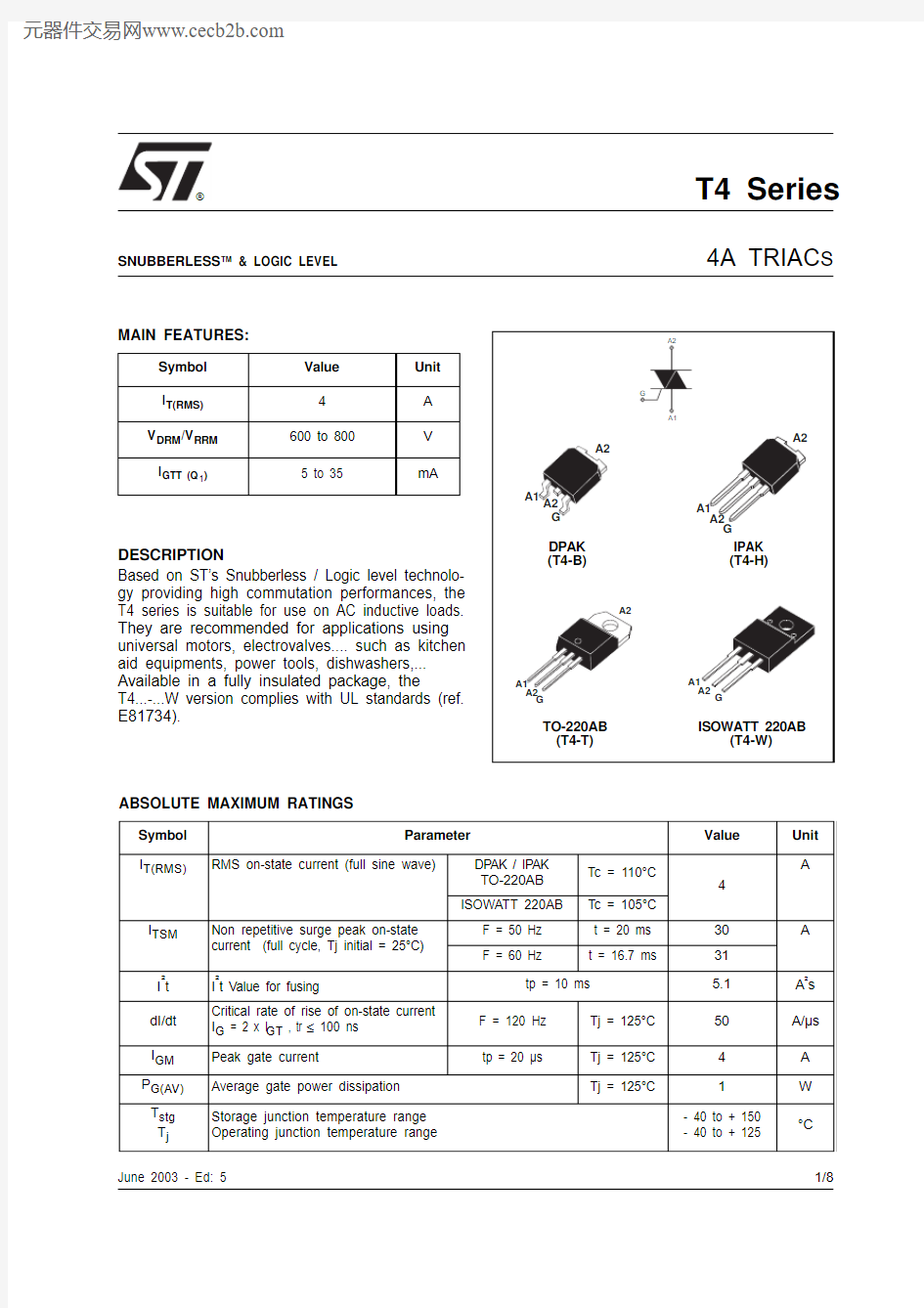
MAIN FEATURES:
DESCRIPTION
Based on ST’s Snubberless / Logic level technolo-gy providing high commutation performances, the T4 series is suitable for use on AC inductive loads.They are recommended for applications using universal motors, electrovalves.... such as kitchen aid equipments, power tools, dishwashers,...
Available in a fully insulated package, the T4...-...W version complies with UL standards (ref.E81734).
Symbol Value Unit I T(RMS)4A V DRM /V RRM 600 to 800V I GTT (Q 1)
5 to 35
mA
ABSOLUTE MAXIMUM RATINGS
Symbol Parameter
Value
Unit I T(RMS)
RMS on-state current (full sine wave)
DPAK / IPAK TO-220AB Tc = 110°C 4
A
ISOWATT 220AB
Tc = 105°C I TSM Non repetitive surge peak on-state current (full cycle, Tj initial = 25°C) F = 50 Hz t = 20 ms 30A
F = 60 Hz
t = 16.7 ms
31I 2t I 2t Value for fusing
tp = 10 ms
5.1
A 2s dI/dt Critical rate of rise of on-state current I G = 2 x I GT , tr ≤ 100 ns F = 120 Hz Tj = 125°C 50A/μs I GM Peak gate current
tp = 20 μs
Tj = 125°C 4A P G(AV)Average gate power dissipation Tj = 125°C
1W T stg T j
Storage junction temperature range Operating junction temperature range
- 40 to + 150- 40 to + 125
°C
T4 Series
2/8
ELECTRICAL CHARACTERISTICS (Tj = 25°C, unless otherwise specified)
STATIC CHARACTERISTICS
Note 1: minimum IGT is guaranted at 5% of IGT max.Note 2: for both polarities of A2 referenced to A1
THERMAL RESISTANCES
S = Copper surface under tab
Symbol Test Conditions
Quadrant
T4Unit
T405
T410T435I GT (1)V D = 12 V R L = 30 ?I - II - III MAX.5
1035
mA V GT I - II - III MAX. 1.3V V GD V D = V DRM R L = 33 k ?Tj = 125°C I - II - III
MIN.0.2V I H (2)I T = 100 mA MAX.101535mA I L I G = 1.2 I GT
I - III MAX.
102550mA II
153060dV/dt (2)
V D = 67 %V DRM gate open Tj = 125°C MIN.2040400V/μs (dI/dt)c (2)(dV/dt)c = 0.1 V/μs Tj = 125°C
MIN.
1.8
2.7-A/ms
(dV/dt)c = 10 V/μs Tj = 125°C 0.9 2.0-Without snubber Tj = 125°C
-- 2.5
Symbol Test Conditions
Value Unit V TM (2)I TM = 5.5 A tp = 380 μs Tj = 25°C MAX. 1.6V V to (2)Threshold voltage Tj = 125°C MAX.0.9V R d (2)Dynamic resistance Tj = 125°C MAX.120m ?I DRM I RRM
V DRM = V RRM
Tj = 25°C MAX.
5μA Tj = 125°C
1
mA
Symbol Parameter
Value Unit R th(j-c)
Junction to case (AC)
DPAK IPAK TO-220AB 2.6°C/W
ISOWATT220AB
4.0R th(j-a)
Junction to ambient
S = 0.5 cm 2
DPAK 70°C/W
TO-220AB ISOWATT220AB
60IPAK
100
T
T4 Series
3/8
PRODUCT SELECTOR
ORDERING INFORMATION
OTHER INFORMATION
Note: xx = sensitivity, yyy = voltage
Part Number
Voltage (xxx)Sensitivity
Type
Package
600 V
700 V 800 V T405-xxxB X X X 5 mA Logic level DPAK T405-xxxH X X X 5 mA Logic level IPAK T405-xxxT X X X 5 mA Logic level TO-220AB T405-xxxW X X X 5 mA Logic level ISOWATT220AB
T410-xxxB X X X 10 mA Logic level DPAK T410-xxxH X X X 10 mA Logic level IPAK T410-xxxT X X
X 10 mA Logic level TO-220AB T410-xxxW X X X 10 mA Logic level ISOWATT220AB
T435-xxxB X X X 35 mA Snubberless DPAK T435-xxxH X X X 35 mA Snubberless IPAK T435-xxxT X X X 35 mA Snubberless TO-220AB T435-xxxW
X
X
X
35 mA
Snubberless
ISOWATT220AB
Part Number
Marking
Weight Base quantity Packing mode T4xx-yyyB T4xxyyyB 0.3 g 75Tube T4xx-yyyB-TR T4xxyyyB 0.3 g 2500Tape & reel T4xx-yyyH T4xxyyy 0.4 g 75Tube T4xx-yyyT T4xxyyyT 2.3 g 50Tube T4xx-yyyW
T4xxyyyW
2.1 g
50
Tube
T4 Series
4/8
Fig. 1: Maximum power dissipation versus RMS on-state current (full cycle).
Fig. 2-1: RMS on-state current case versus tem-perature (full cycle).
Fig. 2-2: RMS on-state current versus ambient temperature (printed circuit FR4, copper thick-ness: 35μm),full cycle.
Fig. 3: Relative variation of thermal impedance versus pulse duration.
Fig. 4: Relative variation of gate trigger current,holding current and latching current versus junction temperature (typical values).
Fig. 5: Surge peak on-state current versus number of cycles.
T4 Series
5/8
Fig. 6: Non-repetitive surge peak on-state current for a sinusoidal pulse with width tp <10ms, and corresponding value of I2t.
Fig. 7: On-state characteristics (maximum values).
Fig. 8: Relative variation of critical rate of decrease of main current versus (dV/dt)c (typical values).
Fig. 9: Relative variation of critical rate of decrease of main current versus junction temperature.
Fig. 10: DP AK thermal resistance junction to ambient versus copper surface under tab (printed circuit board FR4, copper thickness: 35μm).
T4 Series
PACKAGE MECHANICAL DATA
FOOTPRINT DIMENSIONS (in millimeters)
6/8
T4 Series PACKAGE MECHANICAL DATA
PACKAGE MECHANICAL DATA
7/8
T4 Series
PACKAGE MECHANICAL DATA
Information furnished is believed to be accurate and reliable. However, STMicroelectronics assumes no responsibility for the consequences of use of such information nor for any infringement of patents or other rights of third parties which may result from its use. No license is granted by implication or otherwise under any patent or patent rights of STMicroelectronics. Specifications mentioned in this publication are subject to change without notice. This publication supersedes and replaces all information previously supplied. STMicroelectronics products are not authorized for use as critical components in life support devices or systems without express written approval of STMicroelectronics.
? The ST logo is a registered trademark of STMicroelectronics
? 2003 STMicroelectronics - Printed in Italy - All Rights Reserved
STMicroelectronics GROUP OF COMPANIES
Australia - Brazil - China - Finland - France - Germany - Hong Kong - India - Italy - Japan - Malaysia
Malta - Morocco - Singapore - Spain - Sweden - Switzerland - United Kingdom - U.S.A
https://www.360docs.net/doc/803921920.html,
8/8