USB_3.1 specification 规范
5.3 Connector Mating Interfaces
This section defines the connector mating interfaces, including the connector interface drawings, pin assignments, and descriptions.
5.3.1 USB 3.1 Standard-A Connector
5.3.1.1 Interface Definition
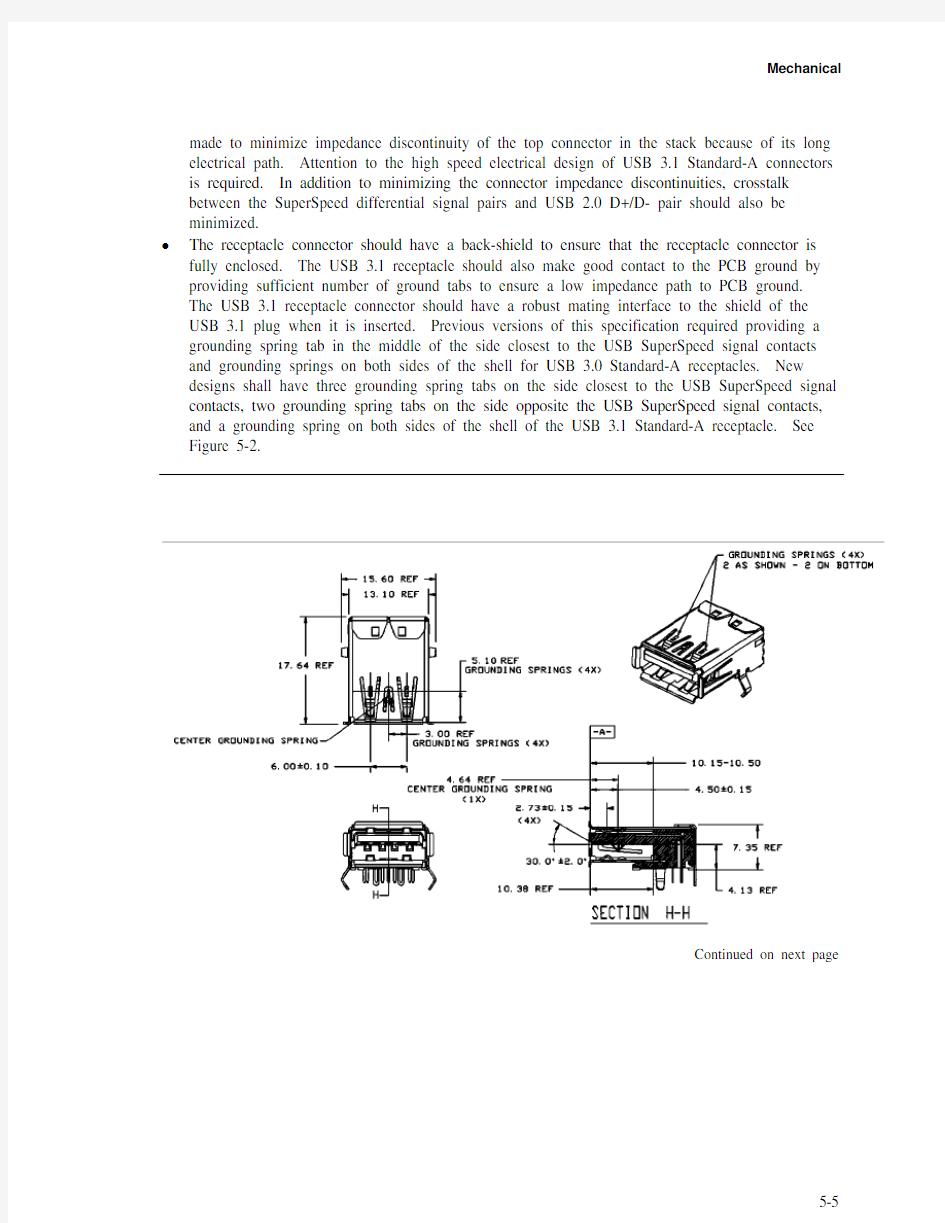
Figure 5-1 and Figure 5-2 show the USB 3.1 Standard-A receptacle and required ground spring
mating areas, respectively. Figure 5-4 shows the Standard-A plug interface dimensions for
USB 3.1. Only the dimensions that govern the mating interoperability are specified. All REF
dimensions are informative.
The Universal Serial Bus Power Delivery Specifiation defines the mechanical and electrical
requirements for the Insertion Detect feature to support cold socket capability. It may be
implemented in a Standard-A receptacle or a PD Standard-A receptacle. Implementation is vendor-specific. The Insertion Detect feature shall be implemented for cold socket Standard-A applications and is optional for all other Standard-A implementations. See the Universal Serial Bus Power
Delivery Specifiation for complete Insertion Detect requirements. Example connector
configurations including Insertion Detect features are shown in Figure 5-3.
Although the USB 3.1 Standard-A connector has basically the same form factor as the USB 2.0
Standard-A connector, it has significant differences inside. Below are the key features and design areas that need attention:
?In addition to the Vbus, D-, D+, and GND pins that are required for USB 2.0, the USB 3.1 Standard-A connector includes five more pins: two differential signal pairs plus one ground
(GND_DRAIN). The two added differential signal pairs are for SuperSpeed data transfer,
supporting dual simplex SuperSpeed signaling. The added GND_DRAIN pin is for drain wire
termination and managing EMI, RFI, and signal integrity.
?The contact areas of the five SuperSpeed pins are located towards the front of the receptacle as blades, while the four USB 2.0 pins towards the back of the receptacle as beams or springs.
Accordingly, in the plug, the SuperSpeed contacts are beams located behind the USB 2.0
blades. In other words, the USB 3.1 Standard-A connector has a two-tier contact system.
?The tiered-contact approach within the Standard-A connector form factor results in less contact area as compared to the USB 2.0 Standard-A connector. The connector interface dimensions
take into consideration contact mating requirements between the USB 3.1 Standard-A
receptacle and USB 3.1 Standard-A plug, the USB 3.1 Standard-A receptacle and USB 2.0
Standard-A plugs, and the USB 2.0 Standard-A receptacles and USB 3.1 Standard-A plug.
?The connector interface definition avoids shorting between the SuperSpeed and USB 2.0 pins during insertion when plugging a USB 2.0 Standard-A plug into a USB 3.1 Standard-A
receptacle or a USB 3.1 Standard-A plug into a USB 2.0 Standard-A receptacle.
?There may be some increase in the USB 3.1 Standard-A receptacle connector depth (into a system board) to support the two-tiered-contacts as compared to the USB 2.0 Standard-A
receptacle.
?Drawings for stacked USB 3.1 Standard-A receptacles are not shown in this specification.
They are allowed as long as they meet all the electrical and mechanical requirements defined in
this specification. When designing a stacked USB 3.1 Standard-A receptacle, efforts need to be 5-4
made to minimize impedance discontinuity of the top connector in the stack because of its long electrical path. Attention to the high speed electrical design of USB 3.1 Standard-A connectors is required. In addition to minimizing the connector impedance discontinuities, crosstalk
between the SuperSpeed differential signal pairs and USB 2.0 D+/D- pair should also be
minimized.
?The receptacle connector should have a back-shield to ensure that the receptacle connector is fully enclosed. The USB 3.1 receptacle should also make good contact to the PCB ground by providing sufficient number of ground tabs to ensure a low impedance path to PCB ground.
The USB 3.1 receptacle connector should have a robust mating interface to the shield of the USB 3.1 plug when it is inserted. Previous versions of this specification required providing a grounding spring tab in the middle of the side closest to the USB SuperSpeed signal contacts and grounding springs on both sides of the shell for USB 3.0 Standard-A receptacles. New designs shall have three grounding spring tabs on the side closest to the USB SuperSpeed signal contacts, two grounding spring tabs on the side opposite the USB SuperSpeed signal contacts, and a grounding spring on both sides of the shell of the USB 3.1 Standard-A receptacle. See Figure 5-2.
Continued on next page
5-5
5-6
Continued on next page
5-7
Figure 5-1. USB 3.1 Standard-A Receptacle Interface Dimensions
TOP VIEW (SIDE NEAREST SUPERSPEED
CONTACTS)
Continued on next page 5-8
5-9
Figure 5-2. Example USB 3.1 Standard-A Receptacle with Grounding Springs and Required
contact zones on the Standard-A Plug.
EMI contact zones
BOTTOM VIEW (SIDE OPPOSITE SUPERSPEED CONTACTS)
Insertion detect pins
Detect circuit is closed after a
mating part is inserted
Detect circuit
Spring fingers on the side of
receptacle shell are EMI functional Array
Figure 5-3. Example USB 3.1 Standard-A Mid-Mount Receptacles with Insertion Detect
5-10
Continued on next page
5-11
Continued on next page 5-12
Figure 5-4. USB 3.1 Standard-A Plug Interface Dimensions
5.3.1.2 USB 3.1 Standard-A Reference Footprints
This specification does not define standard footprints. Any footprint may be used as long as all
mechanical and electrical requirements are met. Example footprints are provided for reference
only.
Figure 5-5 shows through-hole example footprints for the USB 3.1 Standard-A receptacle with a back-shield. Pin numbers are marked.
Figure 5-6 shows an example footprint for a mid-mount standard mount (mounted on the top of the PCB) Standard-A receptacle that includes Insertion Detect.
5-13
Figure 5-7 shows an example mid-mount reverse mount (mounted on the bottom of the PCB) with Insertion Detect. The reverse mount configuration locates the SuperSpeed signals between the USB 2.0 signals and the PCB edge, making the SuperSpeed signal routing more challenging.
See Section 5.6.1.2 for target characteristic impedance.
Continued on next page 5-14
Continued on next page
5-15
Figure 5-5. Example Footprint for the USB 3.1 Standard-A Receptacle - Through-Hole with
Back-Shield
5-16
Figure 5-6. Example Footprint for the USB 3.1 Standard-A Receptacle - Mid-Mount Standard
Mount Through-Hole with Insertion Detect
5-17
Figure 5-7. Example Footprint for the USB 3.1 Standard-A Receptacle - Mid-Mount Reverse
Mount Through-Hole with Insertion Detect
5-18
5.3.1.3 Pin Assignments and Description
The usage and assignments of the nine pins in the USB 3.1 Standard-A connector are defined in Table 5-2.
Table 5-2. USB 3.1 Standard-A Connector Pin Assignments
Pin Number1Signal Name2Description Mating Sequence3
1 VBUS Power Third
2 D- USB 2.0 differential pair Fourth
3 D+
4 GND Ground for power return Third
5 StdA_SSRX- SuperSpeed receiver differential
pair Last
6 StdA_SSRX+
7 GND_DRAIN Ground for signal return
8 StdA_SSTX- SuperSpeed transmitter
differential pair
9 StdA_SSTX+
124, 13 INSERTION
DETECT Receptacle only. Detects
insertion of a plug into the
receptacle. Optional except for
cold socket applications. See the Universal Serial Bus Power
Delivery Specifiation for details.
Second
Shell Shield Connector metal shell First
Note 1: Note 1: Pin numbers not included in this table do not have contacts present.
Note 2: Tx and Rx are defined from the host perspective.
Note 3: The mating sequence assumes support of INSERTION DETECT.
Note 4: Pin 12, if present, shall be connected to Shield.
The physical location of the pins in the connector is illustrated in Figure 5-1 to Figure 5-7. Pins 1 to 4 are referred to as the USB 2.0 pins, while pins 5 to 9 are referred to as the SuperSpeed pins. See the Universal Serial Bus Power Delivery Specifiation for location of pins 12 and 13.
5-19
5-20
5.3.1.4 USB 3.1 Standard-A Connector Color Coding
Since both the USB 2.0 Standard-A and USB 3.1 Standard-A receptacles may co-exist on a host, color coding is recommended for the USB 3.1 Standard-A connector (receptacle and plug) housings to help users distinguish it from the USB 2.0 Standard-A connector.
Blue (Pantone 300C) is the recommended color for the USB 3.1 Standard-A receptacle and plug plastic housings. When the recommended color is used, connector manufacturers and system
integrators should make sure that the blue-colored receptacle housing is visible to users. Figure 5-8 illustrates the color coding recommendation for the USB 3.1 Standard-A connector.
Figure 5-8. Illustration of Color Coding Recommendation for USB 3.1
Standard-A Connector
5.3.2
USB 3.1 Standard-B Connector
5.3.2.1
Interface Definition
Figure 5-9, Figure 5-10, and Figure 5-11 show the USB Standard-B receptacle dimensions, the USB Standard-B plug dimensions, and a USB Standard-B receptacle reference footprint, respectively. See Section 5.6.1.2 for target characteristic impedance.
5-21
Continued on next page
5-22
Figure 5-9. USB 3.1 Standard-B Receptacle Interface Dimensions
5-23
Figure 5-10. USB 3.1 Standard-B Plug Interface Dimensions