LV8401V-TLM-E;中文规格书,Datasheet资料

LV8401V
Overview
The LV8401V is a 1-channel motor driver IC using D-MOS FET for output stage and operates in one of the four modes under program control: forward, reverse, brake, and standby.
As the P/N-channel structure is used in the H-bridge output stage, the LV8401V features minimal number of external component and low on-resistance (0.33? typical). This IC is optimal for driving motors that need large-current.
Functions
? 1-channel forward/reverse motor driver ? Built-in constant current output circuit
? Low power consumption
? Built-in low voltage reset and thermal shutdown circuit ? Low output ON resistance 0.33? ? Four mode function forward/reverse, brake, standby.
Specifications
Maximum Ratings at Ta = 25°C, SGND = PGND = 0V
Parameter Symbol
Conditions
Ratings
Unit
Power supply voltage (for load) VM max -0.5 to 16.0V Power supply voltage (for control) V CC max -0.5 to 6.0
V I O max DC
1.2 A I O peak1 t ≤ 100ms, f = 5Hz
2.0 A I O peak2 t ≤ 10ms, f = 5Hz
3.8 A Output current
I OUT max
DC 30
mA Input voltage
V IN max
-0.5 to V CC +0.5
V Allowable power dissipation Pd max Mounted on a specified board * 800mW Operating temperature Topr -20 to +75°C Storage temperature
Tstg
-55 to +150
°C
* Specified board : 30mm × 50mm × 1.6mm, glass epoxy board.
Bi-CMOS IC
Forward/Reverse Motor Driver
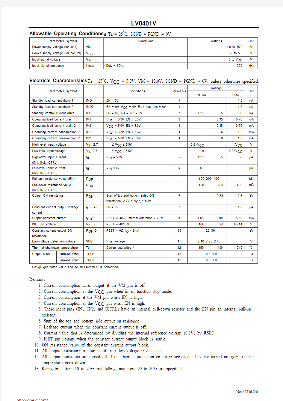
Allowable Operating Conditions at Ta = 25°C, SGND = PGND = 0V
Parameter Symbol Conditions Ratings Unit Power supply voltage (for load) VM 4.0 to 15.0V Power supply voltage (for control) V CC 2.7 to 5.5V Input signal voltage V IN0 to V CC V Input signal frequency f max Duty = 50% 200kHz
Electrical Characteristics Ta = 25°C, V CC = 5.0V, VM = 12.0V, SGND = PGND = 0V, unless otherwise specified.
Ratings Parameter Symbol Conditions Remarks
min typ max
Unit Standby load current drain 1 IMO1 EN = 0V 1 1.0μA Standby load current drain 2 IMO2 EN = 0V, V CC = 0V, Each input pin = 0V 1 1.0μA Standby control current drain ICO EN = 0V, IN1 = IN2 = 0V 2 12.5 25 50μA Operating load current drain 1 IM1 V CC = 3.3V, EN = 3.3V 3 0.35 0.70mA Operating load current drain 2 IM2 V CC = 5.0V, EN = 5.0V 3 0.35 0.70mA Operating current consumption 1 IC1 V CC = 3.3V, EN = 3.3V 4 0.6 1.2mA Operating current consumption 2 IC2 V CC = 5.0V, EN = 5.0V 4 0.8 1.6mA High-level input voltage V IH 2.7
≤ V CC≤ 5.5V 0.6×V CC V CC V Low-level input voltage V IL 2.7
≤ V CC≤ 5.5V 0 0.2×V CC V High-level input current
(IN1, IN2, ICTRL)
I IH V IN = 5.0V 5 12.5 25 50μA
Low-level input current
(IN1, IN2, ICTRL)
I IL V IN = 0V 5 -1.0 μA Pull-up resistance value (EN) R UP100 200 400k?Pull-down resistance value
(IN1, IN2, ICTRL)
R DN100 200 400k?
Output ON resistance R ON Sum of top and bottom sides ON
resistance. 2.7V ≤ V CC≤ 5.5V 6
0.33
0.5?
Constant current output leakage
current
I O LEAK EN = 0V 7 1.0μA
Output constant current I OUT RSET = 40?, Internal reference = 0.2V 8 4.65 5.00 5.35mA
ISET pin voltage V ISET RSET = 40? 9
0.186
0.20
0.214V
Constant current output ON resistance R ON IO RSET = 0?, I O=
5mA 10 20 30?
Low-voltage detection voltage VCS V CC voltage 11 2.10 2.25 2.40V Thermal shutdown temperature Tth Design guarantee * 12 150 180 210°C Turn-on
time
TPLH 13 0.5 1.0μs Output block
Turn-off
time
TPHL 13 0.5 1.0μs
* Design guarantee value and no measurement is performed.
Remarks
1. Current consumption when output at the VM pin is off.
2. Current consumption at the V CC pin when in all function stop mode.
3. Current consumption at the VM pin when EN is high.
4. Current consumption at the V CC pin when EN is high.
5. These input pins (IN1, IN2, and ICTRL) have an internal pull-down resistor and the EN pin an internal pull-up
resistor.
6. Sum of the top and bottom side output on resistance.
7. Leakage current when the constant current output is off.
8. Current value that is determined by dividing the internal reference voltage (0.2V) by RSET.
9. ISET pin voltage when the constant current output block is active.
10. ON resistance value of the constant current output block.
11. All output transistors are turned off if a low-voltage is detected.
12. All output transistors are turned off if the thermal protection circuit is activated. They are turned on again as the
temperature goes down.
13. Rising time from 10 to 90% and falling time from 90 to 10% are specified.
Package Dimensions
unit : mm (typ) 3178B
Pin Assignment
V CC IN1VM
123
456
78
IN2EN ICTRL ISET SGND IOUT 161514131211109OUT1OUT1PGND PGND OUT2
OUT2VM Top view
LV8401V
Ambient temperature, Ta -- °C
A l l o w a b l e p o w e r d i s s i p a t i o n , P d m a x -- W
Block Diagram
OUT1
OUT2
PGND IOUT
ISET SGND
VM
IN1
V CC
IN2
ICTRL
EN
Truth Table
EN IN1 IN2 OUT1 OUT2 Mode
H H L L
Brake
H L H L Forward L H L H Reverse H
L L Z Z Standby
L
- - Z Z
All function stop
EN ICTRL IOUT Mode
H ON Constant current ON H L Z Constant current OFF L
-
Z
All function stop
- : denotes a don't care value. Z : High-impedance
? Current drain is zero in all function stop mode. (excluding the current that flows out of the EN pin)
* All power transistors turn off and the motor stops driving when the IC is detected in low voltage or thermal protection mode.
Sample Application Circuit
*1 : Connect a kickback absorbing capacitor as close as possible to the IC. Characteristics deterioration of the IC or damage may result if an instantaneous voltage surge exceeding the maximum rated value is applied to the VM line due to coil kickback or other causes.
*2 : The output constant current (I OUT) is determined by the internal reference voltage and the sense resistor between the ISET and SGND pins.
I OUT = Internal reference voltage (0.2V) ÷ Sense resistor (RSET)
From the formula above, I OUT = 5mA when a sense resistor of 40? is connected between the ISET and SGND.
This catalog provides information as of December, 2008. Specifications and information herein are subject
to change without notice.
分销商库存信息: ONSEMI
LV8401V-TLM-E