BAV20-TR中文资料
BAV17/18/19/20/21
Document Number 85543Rev. 1.7, 19-Feb-07
Vishay Semiconductors
https://www.360docs.net/doc/946421364.html,
1
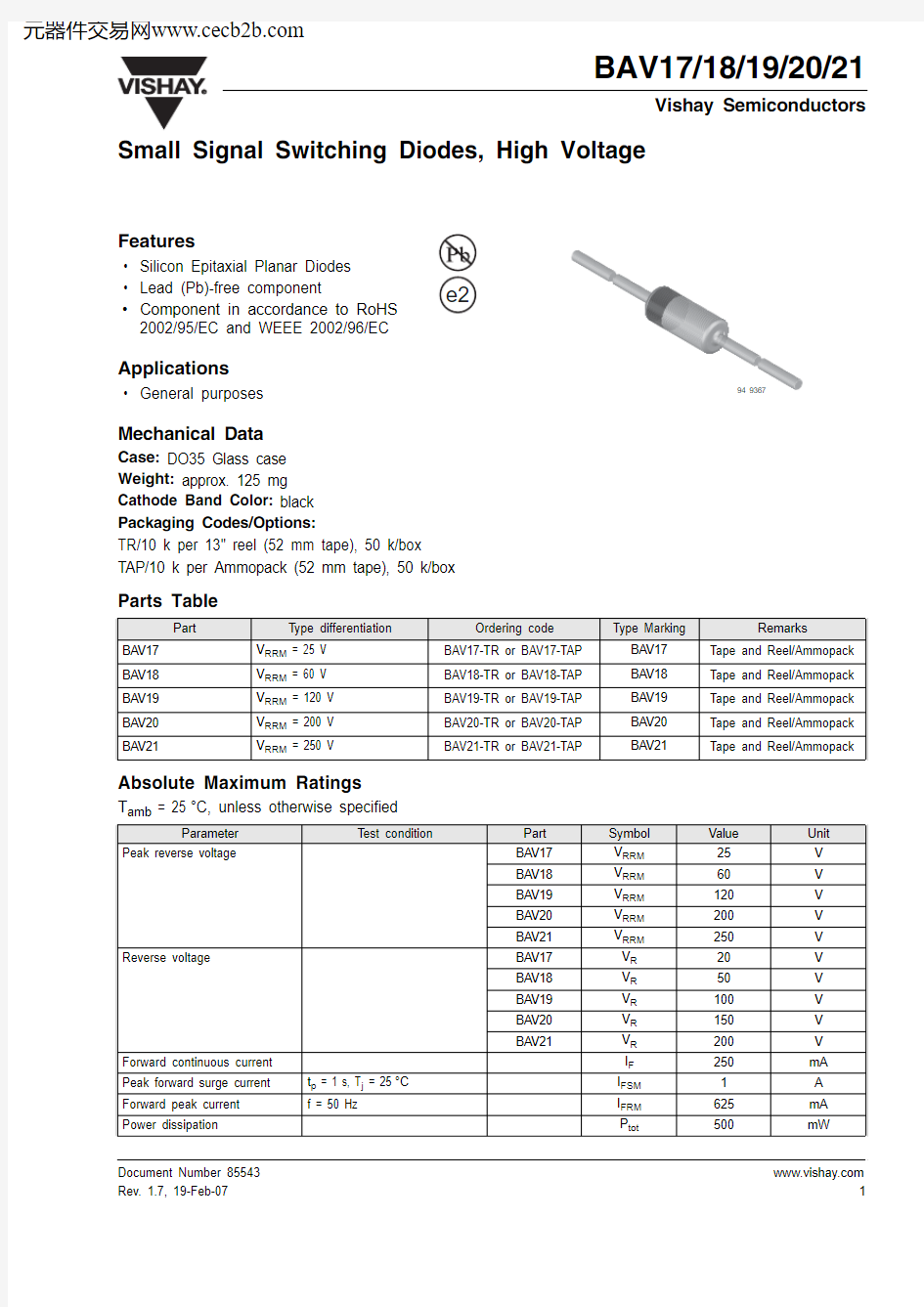
94 9367
Small Signal Switching Diodes, High Voltage
Features
?Silicon Epitaxial Planar Diodes ?Lead (Pb)-free component ?Component in accordance to RoHS 2002/95/EC and WEEE 2002/96/EC
Applications
?General purposes
Mechanical Data
Case: DO35 Glass case Weight: approx. 125 mg Cathode Band Color: black Packaging Codes/Options:
TR/10 k per 13" reel (52 mm tape), 50 k/box
TAP/10 k per Ammopack (52 mm tape), 50 k/box
Parts Table
Absolute Maximum Ratings
T amb = 25°C, unless otherwise specified
Part
T ype differentiation Ordering code Type Marking Remarks
BAV17V RRM = 25 V BAV17-TR or BAV17-TAP BAV17Tape and Reel/Ammopack BAV18V RRM = 60 V BAV18-TR or BAV18-TAP BAV18Tape and Reel/Ammopack BAV19V RRM = 120 V BAV19-TR or BAV19-TAP BAV19Tape and Reel/Ammopack BAV20V RRM = 200 V BAV20-TR or BAV20-TAP BAV20Tape and Reel/Ammopack BAV21
V RRM = 250 V
BAV21-TR or BAV21-TAP
BAV21
Tape and Reel/Ammopack
Parameter
T est condition
Part
Symbol Value Unit Peak reverse voltage
BAV17V RRM 25V BAV18V RRM 60V BAV19V RRM 120V BAV20V RRM 200V BAV21
V RRM 250V Reverse voltage
BAV17V R 20V BAV18V R 50V BAV19V R 100V BAV20V R 150V BAV21
V R 200V Forward continuous current I F 250mA Peak forward surge current t p = 1 s, T j = 25°C I FSM 1A Forward peak current f = 50 Hz
I FRM 625mA Power dissipation
P tot
500
mW
https://www.360docs.net/doc/946421364.html, 2
Document Number 85543
Rev. 1.7, 19-Feb-07
BAV17/18/19/20/21
Vishay Semiconductors Thermal Characteristics
T amb = 25°C, unless otherwise specified
Electrical Characteristics
T amb = 25°C, unless otherwise specified
Parameter
Test condition
Symbol Value Unit Junction to ambient air l = 4 mm, T L = constant
R thJA 300K/W Junction temperature T j 175°C Storage temperature range
T stg
- 65 to + 175
°C
Parameter
Test condition
Part
Symbol Min
Typ.
Max Unit Forward voltage I F = 100 mA V F 1000mV Reverse current
V R = 20 V BAV17I R 100nA V R = 50 V BAV18I R 100nA V R = 100 V BAV19I R 100nA V R = 150 V BAV20I R 100nA V R = 200 V
BAV21I R 100nA T j = 100°C, V R = 20 V BAV17I R 15μA T j = 100°C, V R = 50 V BAV18I R 15μA T j = 100°C, V R = 100V BAV19I R 15μA T j = 100°C, V R = 150 V BAV20I R 15μA T j = 100°C, V R = 200 V
BAV21I R 15
μA Breakdown voltage
I R = 100 μA, t p /T = 0.01, t p = 0.3 ms
BAV17V (BR)25V BAV18V (BR)60V BAV19V (BR)120V BAV20V (BR)200V BAV21
V (BR)250
V Diode capacitance
V R = 0, f = 1 MHz C D 1.5pF Differential forward resistance I F = 10 mA r f 5
ΩReverse recovery time
I F = I R = 30 mA, i R = 3 mA, R L = 100 Ω
t rr
50
ns
BAV17/18/19/20/21
Document Number 85543Rev. 1.7, 19-Feb-07
Vishay Semiconductors
https://www.360docs.net/doc/946421364.html,
3
Typical Characteristics
T amb = 25 °C unless otherwise specified
Package Dimensions in millimeters (inches): DO35
Figure 1. Reverse Current vs. Junction Temperature Figure 2. Forward Current vs. Forward Voltage
40
80
120
160
110I -R e v e r s e C u r r e n t (μA )
R T j -J u nction Temperat u re (°C)
200
94 9084
0.4
0.8 1.2 1.60.1
1
10
100
1000
I -F o r w a r d C u r r e n t (m A )
F V F -For w ard V oltage (V )
2.0
94 9085
Figure 3. Differential Forward Resistance vs. Forward Current
0.1
110110
100
r -D i f f e r e n t i a l F o r w a r d R e s i s t a n c e ()
f I F -For w ard C u rrent (mA)
100
94 9089
Ω
https://www.360docs.net/doc/946421364.html, 4Document Number 85543
Rev. 1.7, 19-Feb-07
BAV17/18/19/20/21
Vishay Semiconductors
Ozone Depleting Substances Policy Statement
It is the policy of Vishay Semiconductor GmbH to
1.Meet all present and future national and international statutory requirements.
2.Regularly and continuously improve the performance of our products, processes, distribution and operating
systems with respect to their impact on the health and safety of our employees and the public, as well as their impact on the environment.
It is particular concern to control or eliminate releases of those substances into the atmosphere which are known as ozone depleting substances (ODSs).
The Montreal Protocol (1987) and its London Amendments (1990) intend to severely restrict the use of ODSs and forbid their use within the next ten years. Various national and international initiatives are pressing for an earlier ban on these substances.
Vishay Semiconductor GmbH has been able to use its policy of continuous improvements to eliminate the use of ODSs listed in the following documents.
1.Annex A, B and list of transitional substances of the Montreal Protocol and the London Amendments
respectively
2.Class I and II ozone depleting substances in the Clean Air Act Amendments of 1990 by the Environmental
Protection Agency (EPA) in the USA
3.Council Decision 88/540/EEC and 91/690/EEC Annex A, B and C (transitional substances) respectively. Vishay Semiconductor GmbH can certify that our semiconductors are not manufactured with ozone depleting substances and do not contain such substances.
We reserve the right to make changes to improve technical design
and may do so without further notice.
Parameters can vary in different applications. All operating parameters must be validated for each customer application by the customer. Should the buyer use Vishay Semiconductors products for any unintended or unauthorized application, the buyer shall indemnify Vishay Semiconductors against all claims, costs, damages, and expenses, arising out of, directly or indirectly, any claim of personal damage, injury or death associated with such unintended or unauthorized use.
Vishay Semiconductor GmbH, P.O.B. 3535, D-74025 Heilbronn, Germany
Document Number: 91000
https://www.360docs.net/doc/946421364.html,
Revision: 18-Jul-08
1
Disclaimer
Legal Disclaimer Notice
Vishay
All product specifications and data are subject to change without notice.
Vishay Intertechnology, Inc., its affiliates, agents, and employees, and all persons acting on its or their behalf (collectively, “Vishay”), disclaim any and all liability for any errors, inaccuracies or incompleteness contained herein or in any other disclosure relating to any product.
Vishay disclaims any and all liability arising out of the use or application of any product described herein or of any information provided herein to the maximum extent permitted by law. The product specifications do not expand or otherwise modify Vishay’s terms and conditions of purchase, including but not limited to the warranty expressed therein, which apply to these products.
No license, express or implied, by estoppel or otherwise, to any intellectual property rights is granted by this document or by any conduct of Vishay.
The products shown herein are not designed for use in medical, life-saving, or life-sustaining applications unless otherwise expressly indicated. Customers using or selling Vishay products not expressly indicated for use in such applications do so entirely at their own risk and agree to fully indemnify Vishay for any damages arising or resulting from such use or sale. Please contact authorized Vishay personnel to obtain written terms and conditions regarding products designed for such applications.
Product names and markings noted herein may be trademarks of their respective owners.
元器件交易网https://www.360docs.net/doc/946421364.html,