HBT169M中文资料
Page No. : 1/4
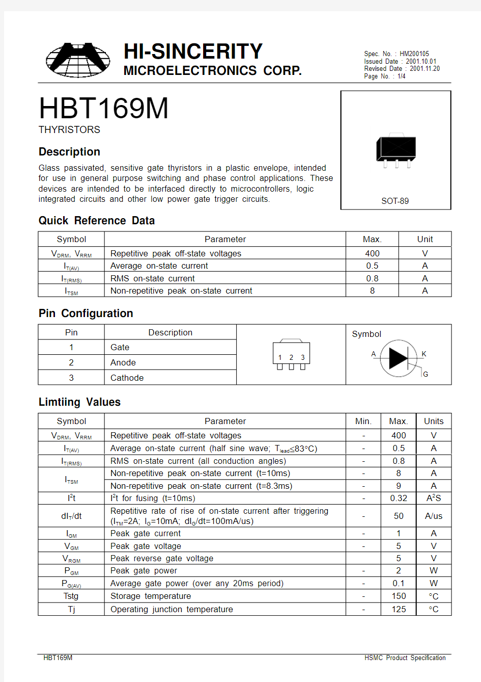
HBT169M
THYRISTORS
Description
Glass passivated, sensitive gate thyristors in a plastic envelope, intended for use in general purpose switching and phase control applications. These devices are intended to be interfaced directly to microcontrollers, logic integrated circuits and other low power gate trigger circuits.
Quick Reference Data
Symbol Parameter
Max.Unit V DRM , V RRM
Repetitive peak off-state voltages 400V I T(AV)Average on-state current 0.5A I T(RMS)RMS on-state current
0.8A I TSM
Non-repetitive peak on-state current
8
A
Pin Configuration
Limtiing Values
Symbol Parameter
Min.Max.Units V DRM , V RRM
Repetitive peak off-state voltages
-400V I T(AV)Average on-state current (half sine wave; T lead ≤83°C)-0.5A I T(RMS)
RMS on-state current (all conduction angles)-0.8A Non-repetitive peak on-state current (t=10ms)-8
A I TSM Non-repetitive peak on-state current (t=8.3ms)-9A I 2t I 2t for fusing (t=10ms)
-0.32A 2S dI T /dt Repetitive rate of rise of on-state current after triggering (I TM =2A; I G =10mA; dI G /dt=100mA/us)-50A/us I GM Peak gate current -1A V GM Peak gate voltage
-5V V RGM Peak reverse gate voltage 5V P GM Peak gate power
-2W P G(AV)Average gate power (over any 20ms period)-0.1W Tstg Storage temperature
-150°C Tj
Operating junction temperature
-125
°C
Page No. : 2/4 Thermal Resistances
Symbol Parameter Conditions Min.Typ.Max.Unit
Rth j-lead Thermal resistance junction to lead Rth j-a Thermal resistance junction to ambient pcb mounted;
lead length=4mm
-
-
-
150
60
-
K/W
K/W
Static Characteristics (Ta=25°C)
Symbol Parameter Conditions Min.Typ.Max.Unit
I GT Gate Trigger Current V D=12V, I T=10mA
Gate open circuit
-50200uA
I L Latching Current V
D
=12V, I GT=0.5mA; R GK=1k?-26mA
I H Holding Current V
D
=12V, I GT=0.5mA; R GK=1k?-25mA V T On-state Voltage I T=1A- 1.2 1.35V
V D=12V, I T=10mA Gate open circuit -0.50.8V
V GT Gate Trigger Voltage
V D= V DRM(max), I T=10mA; Tj=125°C
Gate open circuit
0.20.2-V
I D,I R Off-state Leakage
Current
V D=V DRM(max); V R= V RRM(max);
Tj=125°C; R GK=1k?
-0.050.1mA
Static Characteristics
Symbol Parameter Conditions Min.Typ.Max.Unit
dV D/dt Critical rate of rise of
off-state voltage
V DM=67% V DRM(max); Tj=125°C
exponential waveform; R GK=1k?
500800-V/us
tgt Gate controlled turn-on
time
I TM=2A; V D=V DRM(max)
I G=10mA; dI G/dt=0.1A/us
-2-us
tq Circuit commutated
turn-off time
V D=67% V DRM(max); Tj=125°C
I TM=1.6A; V R=35V; dI TM/dt=30A/us
dV D/dt=2V/us; R GK=1k?
-100-us
Page No. : 3/4
Characteristics Curve
Page No. : 4/4 SOT-89 Dimension
Important Notice:
? All rights are reserved. Reproduction in whole or in part is prohibited without the prior written approval of HSMC.
? HSMC reserves the right to make changes to its products without notice.
?HSMC semiconductor products are not warranted to be suitable for use in Life-Support Applications, or systems.
? HSMC assumes no liability for any consequence of customer product design, infringement of patents, or application assistance. Head Office And Factory:
?Head Office (Hi-Sincerity Microelectronics Corp.): 10F.,No. 61, Sec. 2, Chung-Shan N. Rd. Taipei Taiwan R.O.C.
Tel: 886-2-25212056 Fax: 886-2-25632712, 25368454
?Factory 1: No. 38, Kuang Fu S. Rd., Fu-Kou Hsin-Chu Industrial Park Hsin-Chu Taiwan. R.O.C
Tel: 886-3-5983621~5 Fax: 886-3-5982931