CS-221342-DS-3-CSR8811A08 0.5mm WLCSP DataSheet
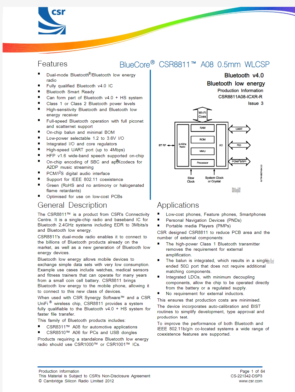

Features BlueCore ? CSR8811? A08 0.5mm WLCSP
■Dual-mode Bluetooth ?/Bluetooth low energy
radio ■Fully qualified Bluetooth v4.0 IC ■Bluetooth Smart Ready ■Can form part of Bluetooth v4.0 + HS system ■Class 1 or Class 2 Bluetooth power levels ■High-sensitivity Bluetooth and Bluetooth low
energy receiver
■Full-speed Bluetooth operation with full piconet
and scatternet support
■On-chip balun and minimal BOM
■Low-power selectable 1.2 to 3.6V I/O
■Integrated I/O and core regulators
■High-speed UART port (up to 4Mbps)
■HFP v1.6 wide-band speech supported on-chip
■On-chip encoding of SBC and aptX ? codecs for
A2DP music streaming
■PCM/I 2S digital audio interface
■Support for IEEE 802.11 coexistence
■Green (RoHS and no antimony or halogenated
flame retardants)
■Optimised for use on low-cost PCBs
Bluetooth v4.0
Bluetooth low energy
Production Information
CSR8811A08-ICXR-R
Issue 3
General Description The CSR8811? is a product from CSR's Connectivity Centre. It is a single-chip radio and baseband IC for Bluetooth 2.4GHz systems including EDR to 3Mbits/s and Bluetooth low energy.CSR8811's dual-mode radio enables it to connect to the billions of Bluetooth products already on the market, as well as a new generation of Bluetooth low energy devices.Bluetooth low energy allows mobile devices to exchange simple data sets with very low consumption.Example use cases include watches, medical sensors and fitness trainers that can operate for many years from a small coin cell battery. CSR8811 brings Bluetooth low energy to the mobile phone, allowing it to connect to this new class of devices.When used with CSR Synergy Software? and a CSR UniFi ? wireless chip, CSR8811 provides a system fully qualifiable to the Bluetooth v4.0 + HS system for faster file transfer.
This family of Bluetooth products includes:■CSR8311? A08 for automotive applications ■CSR8510? A06 for PCs and USB dongles Products requiring a standalone Bluetooth low energy radio should use CSR1000? or CSR1001? ICs.
Applications
■Low-cost phones, Feature phones, Smartphones
■
Personal Navigation Devices (PNDs)
■Portable media Players (PMPs)
CSR designed CSR8811 to reduce PCB area and the
number of external components:
■The high-power Class 1 Bluetooth transmitter
removes the requirement for external
amplification.
■The balun is integrated, which results in a single-
ended 50Ω port that does not require additional
matching components.
■Integrated LDOs, with minimum decoupling
components, allow the chip to be operated directly
from the battery or a regulated supply.
■No requirement for external inductors.
This ensures that production costs are minimised.
The device incorporates auto-calibration and BIST
routines to simplify development, type approval and
production test.
To improve the performance of both Bluetooth and
IEEE 802.11b/g/n co-located systems a wide range of
coexistence features are supported.
CSR8811 A08 0.5mm pitch WLCSP
Data Sheet
Device Details
Bluetooth low energy
■Dual mode Bluetooth low energy radio
■Supports simultaneous Bluetooth BR/EDR and multiple low energy connections
■Support for on-chip AES encryption
■Adaptive Bluetooth/Bluetooth low energy scheduler ■On-chip whitelist support
Bluetooth Radio
■On-chip balun (50Ω impedance in TX and RX modes)
■No external trimming is required in production
■Bluetooth v4.0 specification compliant
Bluetooth Transmitter
■Class 1, Class 2 and Class 3 support without need for external power amplifier or TX/RX switch
■DQPSK and 8DPSK
Bluetooth Receiver
■Integrated channel filters
■Digital demodulator for improved sensitivity and co-channel rejection
■Real time digitised RSSI available on HCI interface ■Fast AGC for enhanced dynamic range
■Channel classification for AFH
■DQPSK and 8DPSK
Baseband and Software
■Internal RAM allows full-speed data transfer, mixed voice and data, and full piconet operation, including all medium rate packet types
■Logic for forward error correction, header error control, access code correlation, CRC,
demodulation, encryption bit stream generation,
whitening and transmit pulse shaping. Includes
support for eSCO and AFH
■Transcoders for A-law, μ-law and linear voice from host and A-law, μ-law and CVSD voice over air Bluetooth Stack
■CSR's Bluetooth Protocol Stack runs on the on-chip
MCU in the configuration Standard HCI over UART Synthesiser
■Fully integrated synthesiser requires no external
VCO varactor diode, resonator or loop filter
■Compatible with external clock 19.2MHz to 40MHz
■Can be operated from external crystal
Physical Interfaces
■UART interface with programmable baud rate up to
4Mbits/s
■BCSP, H4, H4DS and H5 support
■PCM/I2S interface
■Synchronous serial interface up to 4Mbits/s for
system debugging
Auxiliary Features
■Power management includes digital shutdown, and
wake up commands with an integrated low power
oscillator for ultra low power Park/Sniff/Hold mode
■Auto Baud Rate setting, depending on host
interface
■On-chip linear regulators:
■ 1.8V output from typical 2.5 to 4.8V (5.5V for
short periods) input (load current 100mA)
■Low dropout linear regulators producing
internal supply voltages from 1.8V, and
allowing operation directly from a battery
■Power-on-reset cell detects low supply voltage
■Arbitrary sequencing of power supplies is permitted
Package
■28-ball 2.57 x 3.21 x 0.6mm, 0.5mm pitch WLCSP
Note:
This IC has the same package size as the
previous CSR8811 WLCSP 0.5mm pitch
versions and the CSR8810 WLCSP 0.5mm
pitch ICs.
■Can be used on low-cost PCBs without the need for
blind vias
CSR8811 A08 0.5mm pitch WLCSP
Data Sheet
Document History
CSR8811 A08 0.5mm pitch WLCSP
Data Sheet
Status Information
The status of this Data Sheet is Production Information.
CSR Product Data Sheets progress according to the following format:
Advance Information
Information for designers concerning CSR product in development. All values specified are the target values of the design. Minimum and maximum values specified are only given as guidance to the final specification limits and must not be considered as the final values.
All detailed specifications including pinouts and electrical specifications may be changed by CSR without notice. Pre-production Information
Pinout and mechanical dimension specifications finalised. All values specified are the target values of the design. Minimum and maximum values specified are only given as guidance to the final specification limits and must not be considered as the final values.
All electrical specifications may be changed by CSR without notice.
Production Information
Final Data Sheet including the guaranteed minimum and maximum limits for the electrical specifications.
Production Data Sheets supersede all previous document versions.
Life Support Policy and Use in Safety-critical Applications
CSR's products are not authorised for use in life-support or safety-critical applications. Use in such applications is done at the sole discretion of the customer. CSR will not warrant the use of its devices in such applications.
CSR Green Semiconductor Products and RoHS Compliance
CSR8811 devices meet the requirements of Directive 2002/95/EC of the European Parliament and of the Council on the Restriction of Hazardous Substance (RoHS).
CSR8811 devices are also free from halogenated or antimony trioxide-based flame retardants and other hazardous chemicals. For more information, see CSR's Environmental Compliance Statement for CSR Green Semiconductor Products.
Trademarks, Patents and Licences
Unless otherwise stated, words and logos marked with ? or ? are trademarks registered or owned by CSR plc or its affiliates. Bluetooth ? and the Bluetooth ? logos are trademarks owned by Bluetooth ? SIG, Inc. and licensed to CSR. Other products, services and names used in this document may have been trademarked by their respective owners.
The publication of this information does not imply that any license is granted under any patent or other rights owned by CSR plc and/or its affiliates.
CSR reserves the right to make technical changes to its products as part of its development programme.
While every care has been taken to ensure the accuracy of the contents of this document, CSR cannot accept responsibility for any errors.
Refer to https://www.360docs.net/doc/af2030125.html, for compliance and conformance to standards information.CSR8811 A08 0.5mm pitch WLCSP
Data Sheet
Contents
Device Details (2)
Functional Block Diagram (3)
1Package Information (10)
1.1Pinout Diagram (10)
1.2Device Terminal Functions (11)
1.3Package Dimensions (13)
1.4PCB Design and Assembly Considerations (14)
1.5Typical Solder Reflow Profile (14)
2Bluetooth Modem (15)
2.1Bluetooth Radio Ports (15)
2.1.1BT_RF (15)
2.2Bluetooth Receiver (15)
2.2.1Low Noise Amplifier (15)
2.2.2 RSSI Analogue to Digital Converter (15)
2.3RF Transmitter (15)
2.3.1IQ Modulator (15)
2.3.2Power Amplifier (16)
2.4Bluetooth Radio Synthesiser (16)
2.5Baseband (16)
2.5.1Burst Mode Controller (16)
2.5.2Physical Layer Hardware Engine (16)
3Clock Input and Generation (17)
3.1Input Frequencies (17)
3.2External Reference Clock (17)
3.2.1Input: XTAL_IN (17)
3.2.2XTAL_IN Impedance in External Mode (18)
3.2.3Clock Start-up Delay (18)
3.3Crystal Oscillator: SYS_CLK and XTAL_OUT (18)
3.3.1Load Capacitance (20)
3.3.2Frequency Trim (20)
3.3.3Transconductance Driver Model (21)
3.3.4Negative Resistance Model (21)
3.3.5Crystal PS Key Settings (22)
3.4Timing for Frequency (22)
3.5Sleep Clock (22)
4Bluetooth Stack Microcontroller (24)
4.1Programmable I/O Ports (24)
4.2WLAN Coexistence Interface (24)
5Memory Interface and Management (25)
5.1Memory Management Unit (25)
5.2System RAM (25)
5.3Internal ROM Memory (5Mb) (25)
6Host Interface (26)
6.1 UART Interface ................................................................................................................................... 26CSR8811 A08 0.5mm pitch WLCSP
Data Sheet
6.1.1UART Configuration While Reset is Active (27)
7Programming and Debug Interface (28)
8Audio Interfaces (29)
8.1PCM Interface (29)
8.1.1PCM Interface Master/Slave (29)
8.1.2Long Frame Sync (30)
8.1.3Short Frame Sync (31)
8.1.4Multi-slot Operation (31)
8.1.5GCI Interface (32)
8.1.6Slots and Sample Formats (32)
8.1.7Additional Features (33)
8.1.8PCM Timing Information (34)
8.1.9PCM_CLK and PCM_SYNC Generation (38)
8.1.10PCM Configuration (38)
8.2Digital Audio Interface (I2S) (41)
9Power Control and Regulation (46)
9.1High-voltage Linear Regulator (46)
9.1.1Regulator Control (46)
9.2Low-voltage VDD_DIG Linear Regulator (46)
9.3Low-voltage VDD_ANA Linear Regulator (46)
9.4Low-voltage VDD_AUX Linear Regulator (46)
9.5Reset (47)
9.6Power-on Sequencing (47)
10Example Application Schematic (48)
11Electrical Characteristics (49)
11.1Absolute Maximum Ratings (49)
11.2Recommended Operating Conditions (49)
11.3Input/Output Terminal Characteristics (50)
11.3.1High-voltage Linear Regulator (50)
11.3.2Low-voltage VDD_DIG Linear Regulator (50)
11.3.3Low-voltage VDD_AUX Linear Regulator (50)
11.3.4Low-voltage VDD_RADIO Linear Regulator (50)
11.3.5Digital (51)
11.3.6Clock (51)
11.3.7Sleep Clock (52)
11.4ESD Protection (52)
12Software (53)
12.1On-chip Software (53)
12.1.1BlueCore HCI Stack (53)
12.2Off-chip Software (54)
12.2.1CSR Synergy (54)
13CSR Green Semiconductor Products and RoHS Compliance (55)
14Ordering Information (56)
14.1Chip Marking (56)
15Tape and Reel Information (57)
15.1Tape Orientation (57)
15.2Tape Dimensions ................................................................................................................................. 57CSR8811 A08 0.5mm pitch WLCSP
Data Sheet
15.3Reel Information (58)
15.4Moisture Sensitivity Level (59)
16Document References (60)
Terms and Definitions (61)
List of Figures
Figure 1.1Pinout Diagram (10)
Figure 2.1Simplified Circuit BT_RF (15)
Figure 3.1Crystal Driver Circuit (19)
Figure 3.2Crystal Equivalent Circuit (19)
Figure 3.3Example Sleep Clock Application Circuit (23)
Figure 6.1Universal Asynchronous Receiver Transmitter (UART) (26)
Figure 6.2Break Signal (27)
Figure 8.1PCM Interface Master (29)
Figure 8.2PCM Interface Slave (30)
Figure 8.3Long Frame Sync (Shown with 8-bit Companded Sample) (30)
Figure 8.4Short Frame Sync (Shown with 16-bit Sample) (31)
Figure 8.5Multi-slot Operation with 2 Slots and 8-bit Companded Samples (31)
Figure 8.6GCI Interface (32)
Figure 8.716-bit Slot Length and Sample Formats (33)
Figure 8.8PCM Master Timing Long Frame Sync (35)
Figure 8.9PCM Master Timing Short Frame Sync (36)
Figure 8.10PCM Slave Timing Long Frame Sync (37)
Figure 8.11PCM Slave Timing Short Frame Sync (38)
Figure 8.12Digital Audio Interface Modes (43)
Figure 8.13Digital Audio Interface Slave Timing (44)
Figure 8.14Digital Audio Interface Master Timing (45)
Figure 12.1Example Firmware Architecture (53)
Figure 12.2CSR Synergy Framework (54)
Figure 14.1CSR8811A08 Chip Marking (56)
Figure 15.1Tape Orientation (57)
Figure 15.2Tape Dimensions (57)
Figure 15.3Reel Dimensions (58)
List of Tables
Table 3.1External Clock Specifications (17)
Table 3.2Crystal Specification (19)
Table 6.1Possible UART Settings (27)
Table 8.1PCM Master Timing (34)
Table 8.2PCM Master Mode Timing Parameters (34)
Table 8.3PCM Slave Timing (36)
Table 8.4PCM Slave Mode Timing Parameters (37)
Table 8.5PSKEY_PCM_LOW_JITTER_CONFIG Description (39)
Table 8.6PSKEY_PCM_CONFIG32 Description (40)
Table 8.7Alternative Functions of the Digital Audio Bus Interface on the PCM Interface ............................... 41CSR8811 A08 0.5mm pitch WLCSP
Data Sheet
Table 8.8PSKEY_DIGITAL_AUDIO_CONFIG (42)
Table 8.9Digital Audio Interface Slave Timing (44)
Table 8.10I2S Slave Mode Timing (44)
Table 8.11Digital Audio Interface Master Timing (45)
Table 8.12I2S Master Mode Timing Parameters, WS and SCK as Outputs (45)
Table 11.1Sleep Clock Specification (52)
Table 11.2ESD Handling Ratings (52)
Table 15.1Tape Dimensions (58)
Table 15.2Reel Dimensions (58)
List of Equations
Equation 3.1Load Capacitance (20)
Equation 3.2Trim Capacitance (20)
Equation 3.3Frequency Trim (20)
Equation 3.4Pullability (20)
Equation 3.5Transconductance Required for Oscillation (21)
Equation 3.6Equivalent Negative Resistance (21)
Equation 8.1PCM_CLK Frequency Generated Using the Internal 48MHz Clock (38)
Equation 8.2PCM_SYNC Frequency Relative to PCM_CLK (38)
CSR8811 A08 0.5mm pitch WLCSP
Data Sheet
1
Package Information 1.1Pinout Diagram
G
-
T W
-0
04
7
4
.
3
.2
Orientation from top of device
A 124356
B C D E E1C1B1A1E2D2C2B2A2E3D3C3A3E4D4C4B4A4E5D5C5B5A5E6D6
C6
B6
A6
Figure 1.1: Pinout Diagram
CSR8811 A08 0.5mm pitch WLCSP
Data Sheet
1.2Device Terminal Functions
CSR8811 A08 0.5mm pitch WLCSP
Data Sheet
CSR8811 A08 0.5mm pitch WLCSP
Data Sheet
1.4PCB Design and Assembly Considerations
This section lists recommendations to achieve maximum board-level reliability of the 2.57 x 3.21 x 0.6mm WLCSP 28-ball package:
■NSMD lands (that is, lands smaller than the solder mask aperture) are preferred because of the greater accuracy of the metal definition process compared to the solder mask process. With solder mask defined pads, the overlap of the solder mask on the land creates a step in the solder at the land interface, which can cause stress concentration and act as a point for crack initiation.
■Ideally, use via-in-pad technology to achieve truly NSMD lands. Where this is not possible, a maximum of one trace connected to each land is preferred and this trace should be as thin as possible, this needs to take into consideration its current carrying and the RF requirements.
■35μm thick (1oz) copper lands are recommended rather than 17μm thick (0.5oz). This results in a greater standoff which has been proven to provide greater reliability during thermal cycling.
■Use 300μm ±10μm land diameters to achieve optimum reliability.
■Solder paste is preferred to flux during the assembly process, because this adds to the final volume of solder in the joint, increasing its reliability.
■When using a nickel gold plating finish, keep the gold thickness below 0.5μm to prevent brittle gold/tin intermetallics forming in the solder.
■The WLCSP is designed so that ball lands do not lie on top of sensitive areas of the active silicon.■WLCSP components often have the ball array mid-point offset to the centre of the component outline. This requires careful consideration during component PCB footprint design.
1.5Typical Solder Reflow Profile
See Typical Solder Reflow Profile for Lead-free Devices for information.
CSR8811 A08 0.5mm pitch WLCSP
Data Sheet
2Bluetooth Modem
2.1Bluetooth Radio Ports
2.1.1BT_RF
CSR8811 contains an on-chip balun which combines the balanced outputs of the PA on transmit and produces the balanced input signals for the LNA required on receive. No matching components are needed as the receive mode
impedance is 50Ω and the transmitter has been optimised to deliver power in a 50Ω load.
G
-
T W
-0
4
7
99
.
1
.
2
BT_RF
Figure 2.1: Simplified Circuit BT_RF
2.2Bluetooth Receiver
The receiver features a near-zero IF architecture that enables the channel filters to be integrated onto the die.Sufficient out-of-band blocking specification at the LNA input enables the receiver to operate in close proximity to GSM and W-CDMA cellular phone transmitters without being desensitised.
For both basic rate and EDR, an ADC digitises the IF received signal.
2.2.1Low Noise Amplifier
The LNA operates in differential mode and takes its input from the balanced port of the on-chip balun.
2.2.2 RSSI Analogue to Digital Converter
The ADC implements fast AGC. The ADC samples the RSSI voltage on a slot-by-slot basis. The front-end LNA gain is changed according to the measured RSSI value, keeping the mixer input signal within a limited range. This improves the dynamic range of the receiver, so improving performance in interference limited environments.
2.3RF Transmitter
2.3.1IQ Modulator
The transmitter features a direct IQ modulator to minimise frequency drift during a transmit timeslot, which results in a controlled modulation index. Digital baseband transmit circuitry provides the required spectral shaping.
CSR8811 A08 0.5mm pitch WLCSP
Data Sheet
2.3.2Power Amplifier
The internal PA output power is software controlled and configured through a PS Key. The internal PA on the CSR8811 has a maximum output power that enables it to operate as a Class 1, Class 2 and Class 3 Bluetooth radio without requiring an external RF PA.
2.4Bluetooth Radio Synthesiser
The Bluetooth radio synthesiser is fully integrated onto the die with no requirement for an external VCO screening can, varactor tuning diodes, LC resonators or loop filter. The synthesiser is guaranteed to lock in sufficient time across the guaranteed temperature range to meet the Bluetooth v4.0 specification.
2.5Baseband
2.5.1Burst Mode Controller
During transmission the BMC constructs a packet from header information previously loaded into memory-mapped registers by the software and payload data/voice taken from the appropriate ring buffer in the RAM. During reception, the BMC stores the packet header in memory-mapped registers and the payload data in the appropriate ring buffer in RAM. This architecture minimises the intervention required by the processor during transmission and reception.
2.5.2Physical Layer Hardware Engine
Dedicated logic performs the following:
■Forward error correction
■Header error control
■Cyclic redundancy check
■Encryption
■Data whitening
■Access code correlation
■Audio transcoding
Firmware performs the following voice data translations and operations:
■A-law/μ-law/linear voice data (from host)
■A-law/μ-law/CVSD (over the air)
■Voice interpolation for lost packets
■Rate mismatches CSR8811 A08 0.5mm pitch WLCSP
Data Sheet
3Clock Input and Generation
The Bluetooth reference clock for the system is generated from an external clock source frequency of between 19.2and 40MHz, or an external crystal.
All CSR8811 internal digital clocks are generated using a phase locked loop, which is locked to the frequency of the clock source.
3.1Input Frequencies
CSR8811 must be configured to operate with the chosen reference frequency (using the appropriate PS Key, etc.).This can be any reference frequency between 19.2 and 40MHz. Until a clock reference frequency has been explicitly set from an off-chip source no radio operation is possible. This can be done using the debug and programming interface. Otherwise the default, along with various internal firmware checks, enables communication over the host interface for a limited range of baud rates. Once a host communication is established, PS Keys pertaining to the clock scheme can be configured. This depends on the firmware build. Full details are in the Release Note for the CSR8811 firmware build on https://www.360docs.net/doc/af2030125.html, .
3.2External Reference Clock
3.2.1Input: XTAL_IN
CSR8811 can use a TCXO reference clock input into XTAL_IN. In this mode, ground XTAL_OUT.
The external clock can be either a digital level square wave or sinusoidal, and this may be directly coupled to XTAL_IN without the need for additional components. A digital level reference clock gives superior noise immunity, as the high slew rate clock edges have lower voltage to phase conversion. If peaks of the reference clock are either below VSS or above VDD_AUX, it must be driven through a DC blocking capacitor (approximately 33 to 100pF) connected to XTAL_IN.
Table 3.1 lists the specification for the external reference clock signal.
CSR8811 A08 0.5mm pitch WLCSP
Data Sheet
Table 3.1: External Clock Specifications
(a)The frequency should be an integer multiple of 250kHz except for the CDMA/3G frequencies
(b)VDD_AUX is 1.35V nominal
(c)If driven via a DC blocking capacitor max amplitude is reduced to 700mV pk-pk for non 50:50 duty cycle
3.2.2XTAL_IN Impedance in External Mode
The impedance of XTAL_IN does not change significantly between deep sleep and active modes.
3.2.3Clock Start-up Delay
CSR8811 hardware incorporates a default 5ms delay after the assertion of the system clock request signal before running firmware. This is suitable for most applications using an external clock source. However, there are scenarios where the clock is not guaranteed to either exist or be stable after this period. Under these conditions, CSR8811 firmware provides a software function that extends the system clock request signal by a period stored in
PSKEY_CLOCK_STARTUP_DELAY. This value is set in milliseconds from 1ms to 31ms. Zero is the default for 5ms delay.
This PS Key enables system optimisation where clock stability latencies are longer or shorter than 5ms, keeping the current consumption of CSR8811 as low as possible. CSR8811 consumes about 2mA of current for the duration of PSKEY_CLOCK_STARTUP_DELAY before activating the firmware.
Clock accuracy must be within 20ppm after the delay specified in PSKEY_CLOCK_STARTUP_DELAY. This is to ensure that the radio meets the RF specification. Refer to your product software documentation for a description of PSKEY_CLOCK_STARTUP_DELAY.
3.3Crystal Oscillator: SYS_CLK and XTAL_OUT
CSR8811 contains a crystal driver circuit. This operates with an external crystal and capacitors to form a Pierce oscillator. Figure 3.1 shows the external crystal is connected to pins XTAL_IN, XTAL_OUT.CSR8811 A08 0.5mm pitch WLCSP Data Sheet
G
-
T
W
-0
19
1
.5
.
2
Figure 3.1: Crystal Driver Circuit
Figure 3.2 shows an electrical equivalent circuit for a crystal. The crystal appears inductive near its resonant frequency. It forms a resonant circuit with its load capacitors.
Figure 3.2: Crystal Equivalent Circuit The resonant frequency is trimmable with the crystal load capacitance. CSR8811 contains variable internal capacitors to provide a fine trim.
Table 3.2: Crystal Specification
The CSR8811 driver circuit is a transconductance amplifier. A voltage at XTAL_IN generates a current at XTAL_OUT.CSR8811 A08 0.5mm pitch WLCSP
Data Sheet
3.3.1Load Capacitance
For resonance at the correct frequency the crystal should be loaded with its specified load capacitance, which is defined for the crystal. This is the total capacitance across the crystal viewed from its terminals. CSR8811 provides some of this load with the capacitors C trim and C int. The remainder should be from the external capacitors labelled C t1 and C t2. C t1 should be three times the value of C t2 for best noise performance. This maximises the signal swing and slew rate at XTAL_IN (to which all on-chip clocks are referred).
Crystal load capacitance, C l is calculated using Equation 3.1:
C l=C int+(C t2+C trim)C t1 C t2+C trim+C t1
Equation 3.1: Load Capacitance
Note:
C trim = 3.4pF nominal (mid-range setting)
C int = 1.5pF
C int does not include the crystal internal self capacitance; it is the driver self capacitance.
3.3.2Frequency Trim
CSR8811 enables frequency adjustments to be made. This feature is typically used to remove initial tolerance frequency errors associated with the crystal. Frequency trim is achieved by adjusting the crystal load capacitance with an on-chip trim capacitor, C trim. The value of C trim is set by a 6-bit word in PSKEY_ANA_FTRIM. Its value is calculated as follows:
C trim=125fF×PSKEY_ANA_FTRIM
Equation 3.2: Trim Capacitance
The C trim capacitor is connected between XTAL_IN and ground. When viewed from the crystal terminals, the combination of the tank capacitors and the trim capacitor presents a load across the terminals of the crystal which varies in steps of typically 125fF for each least significant bit increment of PSKEY_ANA_FTRIM.
Equation 3.3 describes the frequency trim.
Δ(F x) F x =pullability×0.110×(C t1
C t1+C t2+C trim)(ppm/LSB)
Equation 3.3: Frequency Trim
Note:
F x = crystal frequency
Pullability is a crystal parameter with units of ppm/pF
Total trim range is 0 to 63
If not specified, the pullability of a crystal may be calculated from its motional capacitance with Equation 3.4.
?(F X)?(C l)=F X?
C m
2(C l+C O)2
Equation 3.4: Pullability CSR8811 A08 0.5mm pitch WLCSP
Data Sheet
h3c无线控制器配置
WLAN 目录 目录 第1章 WLAN配置..................................................................................................................1-1 1.1 概述....................................................................................................................................1-1 1.1.1 WLAN的工作机制....................................................................................................1-1 1.1.2 WLAN组网...............................................................................................................1-2 1.1.3 WLAN的协议标准....................................................................................................1-4 1.1.4 WLAN的基本配置项................................................................................................1-4 1.2 配置WLAN.........................................................................................................................1-5 1.2.1 配置概述..................................................................................................................1-5 1.2.2 设置Country Code...................................................................................................1-7 1.2.3 配置WLAN-ESS接口...............................................................................................1-8 1.2.4 配置Radio Policy.....................................................................................................1-8 1.2.5 创建服务模板...........................................................................................................1-9 1.2.6 设置服务模板.........................................................................................................1-10 1.2.7 创建AP模板...........................................................................................................1-10 1.2.8 设置AP参数...........................................................................................................1-10 1.2.9 设置 Radio.............................................................................................................1-11 1.2.10 设置RadioST.......................................................................................................1-11 1.2.11 管理AP&Client.....................................................................................................1-12 1.2.12 获取系统当前AP&Client的详细信息....................................................................1-13 1.3 WLAN典型配置举例.........................................................................................................1-14 1.3.1 Single BSS组网.....................................................................................................1-14 1.3.2 Multiple ESS组网...................................................................................................1-16 1.3.3 WLAN Based on VLAN组网..................................................................................1-19 1.4 注意事项...........................................................................................................................1-22
无线控制器WLC配置
无线控制器(WLC)配置 1.无线控制器WLC的初始配置 连接到WLC的console口,启动超级终端或其它终端软件,把com口属性设置还原为默认值(如下图),点确定应用配置 回车进入命令行管理界面 选择“5. Clear Configuration”,(注意:不同版本的选项顺序不同,要注意查看,而且该处停留时间较短,请及时选择操作序号),清除原有设置,并进行初始设置。 随后根据系统提示完成以下配置: Welcome to the Cisco Wizard Configuration Tool
Use the '-' character to backup System Name [Cisco_40:4a:03]: Enter Administrative User Name (24 characters max): admin //管理员帐号和密码 Enter Administrative Password (24 characters max): ***** Re-enter Administrative Password: ***** Management Interface IP Address: 10.10.11.100 //通过网络远程管理的IP Management Interface Netmask: 255.255.255.0 //掩码 Management Interface Default Router: 10.10.11.1 //管理地址默认路由地址Management Interface VLAN Identifier (0 = untagged): 0 //指定vlan号,0表示WLC工作在vlan 0网段,该vlan 0网段相当于交换机的默认vlan网段,即相当于vlan 1网段。 Management Interface DHCP Server IP Address: 10.10.11.1 //指向DHCP服务器地址,服务器负责DHCP服务功能。 Virtual Gateway IP Address: 1.1.1.1 //cisco推荐的虚拟地址 Mobility/RF Group Name: wuxian Network Name (SSID):wuxian //设置初始wlan Allow Static IP Addresses [YES][no]: yes //允许手工配置IP地址 Configure a RADIUS Server now? [YES][no]: no Enter Country Code list (enter 'help' for a list of countries) [US]: CN //选择中国区域CN Enable 802.11b Network [YES][no]: yes Enable 802.11a Network [YES][no]: yes Enable 802.11g Network [YES][no]: yes //开启802.11a,802.11b,802.11g协议Enable Auto-RF [YES][no]: yes //开启无线射频 Configure a NTP server now? [YES][no]: no Configure the system time now? [YES][no]: yes Enter the date in MM/DD/YY format: //月/日/年,时间设置 ...... Configuration saved! Resetting system with new configuration...
Cisco无线控制器配置
Cisco无线控制器配置 一组网图 System Name [Cisco_01:00:01] (31 characters max):wlc-1//输入设备名称 Would you like to terminate autoinstall? [yes]: //是否终止自动安装,默认是yes #配置管理用户和密码 Enter Administrative User Name (24 characters max): admin Enter Administrative Password (3 to 24 characters): ******** Re-enter Administrative Password : ******** #配置服务接口的IP 注:用于带外管理、系统恢复和维护必须跟带内管理接口在不同子网 Service Interface IP Address Configuration [static][DHCP]: static Service Interface IP Address: 10.10.10.10 Service Interface Netmask: 255.255.255.0 #配置管理接口 注:带内管理接口,可以通过web ssh或者telnet连接的接口,同时也是跟内网其他设备如认证服务器连接的接口 Management Interface IP Address: 192.168.99.250 Management Interface Netmask: 255.255.255.0
Management Interface Default Router: 192.168.99.254 Management Interface VLAN Identifier (0 = untagged): 99 Management Interface Port Num [1 to 1]: 1 Management Interface DHCP Server IP Address: 192.168.99.254 #设置虚拟网关 注:为三层漫游而设置的虚拟接口,在同一个mobility group里的WLC都必须配置相同的虚拟接口 Virtual Gateway IP Address: 1.1.1.1 #配置Mobility/RF Group名称 注:用于用户在不同控制器下的AP间的三层漫游,所以不同控制器的该组必须相同Mobility/RF Group Name: test #配置默认的SSID 注:LAP加入控制器时将使用它,LAP加入后WLC会把其他的SSID提供给LAP Network Name (SSID): test #dhcp桥接 注:Bridging Mode 将会把DHCP 请求透传出去,不做处理;一般都使用WLC本身中继代理功能,默认NO。警告!启用桥接模式将停用内部DHCP服务器和DHCP代理功能。 Configure DHCP Bridging Mode [yes][NO]: no #客户端IP地址配置方式 注:yes为允许客户端使用静态IP,no则为强制客户端使用DHCP来获取IP
振动筛质量标准
产品中心:煤炭行业→ WZDS系列双轴自同步等厚振动筛(法兰式) WZDS系列双轴自同步等厚振动筛工作原理: 两台电动机通过传动轴拖动激振器上的偏心块作反向旋转。两轴上的偏心质量合成的直线或椭圆运动带动筛箱在筛座上经过隔振系统作直线或椭圆运动,物料进入振动着的筛箱在连续不断的抛起前进中以通过筛板达到按颗粒外形大小而分级。 由于双轴自同步椭圆(直线)振动筛没有任何强制同步装置而实现自同步,省去了复杂的同步装置,结构非常简单,操作非常简便。零部件少,故障点少,维修量少,使用成本低。传动路径短,传动部件少,耗能少,节约能源,噪声低。 由于等厚筛分,使物料筛分充分,兼顾筛分效率和处理量。所以筛分效率高,处理量大。 WZDS系列双轴自同步等厚振动筛型号说明: W ZDS □ □ ┬ ┬ ┬ ┬ │ │ │ │ │ │ │ └────────- 筛子长度 │ │ │ │ │ └──────────筛子宽度 │ │ │ └───────────- 等厚振动筛代号 │ └─────────────威猛代号 WZDS系列双轴自同步等厚振动筛安装: 安装前,要检查零部件是否完好、齐全,并对筛机安装基础进行全面清理检查。 安装基础上的预埋钢板和地脚螺栓由用户自备。四个弹簧支承座下的预埋钢板须在同一水平面内。 传动平台的基础应在电动机的高度调整好后,再进行二次浇灌。待隔振架就位,隔振弹簧调整到与
上下支承面均成垂直状态后方可把弹簧座与下部预埋钢板焊牢。焊接时,只许焊弹簧的两侧,不许焊弹簧座的两端。 隔振弹簧在安装前,应对外形尺寸及钢度值进行检查,以保证各组弹簧的刚度和高度保持一致,弹簧安装好后,要求所有的弹簧与上下支撑面保持垂直。 激振器与筛箱在出厂时已装好,并一起发运,安装现场须对原装配情况进行检查,并重新紧固连接件,若安装时已超过设备出厂时间六个月,应将激振器拆开,将各零件清洗后重新安装,在轴承内注入适量的二硫化钼3号锂基脂,一个月加注一次润滑油。重新安装激振器时,要保证同轴各组偏心块的对称中心线在同一平面内。振动器装配完毕后,用转动偏心块,如阻力大或卡死现象。必须找出原因加以调整。 筛机运转时两台电机转向相反。 WZDS系列双轴自同步等厚振动筛使用与维护: 筛机应避免带料起动,起动和运行平稳后再行给料,停车前应先停止给料,待筛面上的物料全部走过后,才能停筛。 工作过程中应经常检查筛机运行是否平稳,若发现运行不正常或有撞击声应立即停车检查。如遇突然事故停机应设法将筛面上的物料排除,以免下次开机时带料起动,影响使用寿命。经常检查筛板与衬板的磨损情况,若发现磨损严重或关键部分出现裂缝,应及时更换或修补。 WZDS系列双轴自同步等厚振动筛技术参数表: WZDS系列双轴自同步等厚振动筛外型尺寸图表:
振动筛技术配置规范
振动筛技术配置规范 一、设计原则 1、振动筛采用椭圆或直线运动轨迹。处理量≥60 L/s,满足正常使用200目以上筛布。 2、振动筛电机为短杆或长杆防爆激振电机。同一系列的振动筛应采用同一电机厂家、同一规格型号的激振电机,并通用互换,宜采用激振力可调激振电机。 3. 使用时间:振动筛不低于8 年。 4、焊接件焊接及检验标准执行国内 JB/T 5943-1991《工程机械焊接件通用技术条件》的相关规定。两联和三联振动筛,应将振动筛与振动筛缓冲罐制造为一整体,以便安装与运输;振动筛缓冲罐宽度一般为400mm,高度一般为1500mm。 两联振动筛底座尺寸一般为L≤3000mm(振动筛长度方向)、W≤4000mm(振动筛宽度方向);三联振动筛底座尺寸一般为L≤3000mm、W≤6000mm。满足现场使用要求和探井安放录井工具的要求。 5、筛分系统宜选用通用型快装板框筛网,要求筛网自身强度高,互换性强、安装拆卸方便,筛网规格为 1165mm×585mm×40 mm,出厂一般配备80目以上筛网(或按需配置)。也可采用勾边筛网,筛网规格:1130×780 mm。 6、筛网与筛床必须使用扣压式安装的全密封结构,密封胶条耐温≥120℃,耐油基泥浆,耐腐蚀性,同时保证密封良好;橡胶件采用耐油橡胶件(丁晴橡胶)并提供第三方证书。 7、不锈钢防飞溅系统,在不影响设备维护的基础上很好的解决钻井液的飞溅问题,保证设备运行现场的清洁舒适。 8、振动筛倾角调节装置采用机械或液压调节装置,实现无级调节,可根据需要动态调节筛箱倾角,以适应不同钻井工况的需要。 9、筛网张紧方式,优先采用楔块快速压紧,可采用螺旋快速张紧装置,筛网更换不超过2分钟/张,宜直接在筛箱外侧拆卸。 10、电机及控制电路符合防爆要求。所有电器设备电源为:380V、50Hz,接线采用三相四线制,TN-S接地型式。防爆级别:Exd II BT4;防护等级:IP55;绝缘等级:155级;电机接线盒的出线口、控制箱进出线口均自带隔爆格兰(黄铜镀镍材料);电机厂家提供合格证、防爆证和IEC证。电路系统使用旋钮控制,
双思科无线控制器冗余配置
WLC故障切换配置(冗余) 为了实现WLC故障切换或冗余,必须完成以下步骤: A.为两台WLC配置移动组. B.为LAP指定主、备WLC C.配置WLC Fallback 特性为2台WLC配置移动组 通过配置移动组可以让无线客户端在一组WLC之间无缝漫游及提供负载均衡和冗余 的功能。如果一台WLC故障,相关联的AP可以自动启动换到移动组中其他WLC 上。当主WLC恢复正常,AP可以重新注册到该台WLC上。故障切换时间为30秒, 这个期间通信将会中断。 提示:所有属于同一个移动组的WLC配置的移动组名字要一致,且大小写敏感。 移动组成员必须包括该组内所有的WLC,以确保可以做到WLC的无缝切换,以及当 主WLC恢复正常,能够让AP重新注册。 本实例移动组包括两台WLC,通过以下步骤配置无线移动组: 1. WLC图形界面下,在上方的菜单下点击进入Controller,然后在左边菜单 选择Mobility Groups .出现窗口Static Mobility Group Members,在这里可以增加
(■VMBBTT DHC F ■4rirtpM l V, *0>*44 iMfH M 4 vis i -t MrtnAnr Tbw Pm I M. *4 QqA IMflBr* 2. 增加一个新的移动组本例只包括两台WLC. a.选择New . b.设定移动组成员IP、MAC以及组名称本实例 第二台WLC的IP为172.16.1.50 , MAC地址为 00:0b:85:33:52:80,移动组为Test. c. 点击Apply . I* A4fa*F*Hr ?■Tlj ■輕側榔 f MM* FI HMI iPfhj^w vl 宇\ —|3t M. I ? I >^4 >4* * K■- wwf ? HI finqp Z?i— (I M ■] Wrvtr 如?I T* Viife* 通过Ping菜单检测移动组成员的连通性 Piw功龍止右上仙卩iy纠采如卜国所示: lM*ff Aa *1 ■[jofilf n|pf
无线控制器WLC配置
无线控制器W L C配置 WTD standardization office【WTD 5AB- WTDK 08- WTD 2C】
无线控制器(W L C)配置无线控制器WLC的初始配置 ?连接到WLC的console口,启动超级终端或其它终端软件,把com口属性设置还原为默认值(如下图),点确定应用配置 ?回车进入命令行管理界面 选择“5. Clear Configuration”,(注意:不同版本的选项顺序不同,要注意查看,而且该处停留时间较短,请及时选择操作序号),清除原有设置,并进行初始设置。 ?随后根据系统提示完成以下配置: Welcome to the Cisco Wizard Configuration Tool Use the '-' character to backupSystem Name [Cisco_40:4a:03]: Enter Administrative User Name (24 characters max): admin .... Configuration saved! Resetting system with new configuration... WLC的WEB网管设置 1.1.登录WEB网管界面 ?通过浏览器地址栏,点击login键,出现登录会话框。 输入用户名和密码:User: admin;Password:****** ?Monitor 页面中的摘要信息,可以看到AP的数量和传输所使用的带宽状态,AP 的管理地址以及WLC的名字,显示如下: 1.2.添加接口Interfaces ?controller页面,左侧点击Interfaces选项,点击右边的new按钮,添加一个新的业务接口地址,相当于建立一个vlan ?填入业务网段的名称vlan 号,点击右上角Apply
ZS型直线振动筛资料
ZS直线振动筛 产品说明 ZS系列直线振动筛利用振动电机激振作为振动源,使物料在筛网上被抛起,同时向前作直线运动,物料从给料机均匀地进入筛分机的进料口,通过多层筛网产生数种规格的筛上物、筛下物、分别从各自的出口排出。具有耗能低、产量高、结构简单、易维修、全封闭结构,无粉尘溢散,自动排料,更适合于流水线作业。 使用范围 对粉状、颗粒状物料的筛选和分级,广泛应用于塑料、磨料、化工、医药、建材、粮食、炭素、化肥等行业
直线振动筛 直线振动筛概述 直线振动筛利用振动电机激振作为振动源,使物料在筛网上被抛起,同时向前作直线运动,物料从给料机均匀地进入筛分机的进料口,通过多层筛网产生数种规格的筛上物、筛下物、分别从各自的出口排出。具有耗能低、产量高、结构简单、易维修、全封闭结构,无粉尘溢散,自动排料,更适合于流水线作业。 直线振动筛工作原理: 直线振动筛采用双振动电机驱动,当两台振动电机做同步、反缶旋转时,其偏心块所产生的激振力在平行于电机轴线的方向相互抵消,在垂直于电机轴的方向叠为一合力,因此筛机的运动轨迹为一直线。其两电机轴相对筛面有一倾角,在激振力和物料自重力的合力作用下,物料在筛面上被抛起跳跃式向前作直线运动,从而达到对物料进行筛选和分级的目的。可用于流水线中实现自动化作业。具有能耗低、效率高、结构简单、易维修、全封闭结构无粉尘溢散的特点。最高筛分目数325目,可筛分出7种不同粒度的物料。 直线振动筛使用范围 对粉状、颗粒状物料的筛选和分级,广泛应用于塑料、磨料、化工、医药、建材、粮食、炭素、化肥等行业. 直线振动筛(直线筛)系高效新型的筛分设备,广泛用于矿山、煤炭、冶炼、建材、耐火材料、轻工、化工等行业。直线振动筛(直线筛)稳定可靠、消耗少、噪音低、寿命长、振型稳、筛分效率高等优点。 直线振动筛技术参数 SZF-520型1S-Q235A或SUS304 2000×500×1200 1层(1S) 2层(2S) 3层(3S) 4层(4S) SZF-525型1S-Q235A或SUS304 2500×500×1200 1层(1S) 2层(2S) 3层(3S) 4层(4S) SZF-825型1S-Q235A或SUS304 2500×800×1200 1层(1S) 2层(2S) 3层(3S) 4层(4S) SZF-820型1S-Q235A或SUS304 2000×800×1200 1层(1S) 2层(2S) 3层(3S) 4层(4S) SZF-1025型1S-Q235A 或SUS304 2500×1000×1500 1层(1S) 2层(2S) 3层(3S) 4层(4S) SZF-1225型1S-Q235A 或SUS304 2500×1200×1500 1层(1S) 2层(2S) 3层(3S) 4层(4S) SZF-1235型1S-Q235A 或SUS304 3500×1200×1600 1层(1S) 2层(2S) 3层(3S) 4层(4S) SZF-1536型1S-Q235A 或SUS304 1500×3600×1200 1层(1S) 2层(2S) 3层(3S) 4层(4S) 使用说明书资料 ☆特点☆ 1)独特之筛网结构设计,方便和快速更换筛网( 只需3到5分钟) ,此外此种设计 允许使用各种筛网( 尼龙、特种龙、PP网)。 2)筛机设计;精巧和容易装配,一人即可操作筛机。 3)和其他相关品牌厂商比较,具较大筛选面积和高效益之处理能力。 4)其母网完全支撑细网,因此细网可独得较长之寿命,而降低细网耗材使用,淤长时间之生产过程可降低诸多成本。 直线振动筛作用与原理 基本原理系借电机轴上下端所安装的重锤(不平蘅重锤),将电机的旋转运动转变为水平、垂直、倾斜的三次元运动,再把这个运动传达给筛面。若改变上下部的重锤的相位角可改变原料的行进方向。
各类型振动筛型号分类及技术参数
精品 型号1: ZS3/Z-01型振动筛 1.用途及适用范围: ZS3/Z-01钻井液振动筛为钻井液中的第一级固控设备,主要用来筛分钻井液中的有害固相颗粒,此钻井液振动筛为三段式直线振动筛,该筛适合油田2000米以上各类钻机的配套使用。 2.结构特点 ▲ZS3/Z-01为三段式筛、直线型振动轨迹筛。 ▲采用2台美国进口MARTIN高G震力长轴激振电机,可在筛网上输出7.3G的震力。振动筛噪音低于78 dBA。 ▲筛箱筛网可配置平板或波浪型结构的钩边筛网,筛网过滤面积大,可适应不同钻井工况下的泥浆处理。 ▲筛网采用压块张紧螺栓拉紧机构,可以快速简便地更换筛网。 ▲筛架为丝杆结构装置,结构简单可靠,可在不间断作业情况,可快速改变筛架-1°~5°的倾角,确保泥浆能合理、有效的得到处理。 ▲筛架支撑减振器采用橡胶复合弹簧,振动效果好,噪音低,使用寿命长。 ZS3/Z-01结构示意图
▲ 此型振动筛结构紧凑,体积轻便,占地面积小, ▲ 振动筛进料器(泥浆盒)与井口溢流管线接口可根据用户选择在泥浆盒的两侧面或背面连 接管线。 技术性能参数 筛网规格 平板或波浪形钩边筛网3-1050×700;筛目:80~200目 激振电机 SVX18-7710 (进口马丁长轴电机):2-1.865KW 最大振动强度 7.1~7.2G 振动幅度: ≥5.5mm 筛箱倾角 -1°~+5° 防爆等级 Exd ⅡBT4 防护等级 IP55 外形尺寸(长×宽×高) 2950×1694×1580mm 重量 1950Kg 筛网面积(㎡) ≥2.3 筛分固相颗粒直径(μm ) ≥75 钻井液处理能力(m3/h ) >200 型号2: ZS3/Z-02型振动筛 1.用途及适用范围: ZS3/Z-02钻井液振动筛为钻井液中的第一级固控设备,主要用来筛分钻井液中的有害固 ZS3/Z-02结构示意图
振动筛的选型资料
1、YZDS型振动筛 一、简介 YZDS系列振动筛为新从国外引进技术,具有当代国际先进水平的一种圆运动振动筛,该系列振动筛广泛适用于冶金、矿山、煤炭、建材、化工、电力、交通、轻工等部门进行各种物料的分级。它具有如下特点: 1、结构新颖,技术参数先进,处理能力大,筛分效率高。 2、采用振动电机作为激振源,使用维修方便。 3、采用弹簧钢编织筛网或冲孔筛板,使用寿命长,不易堵孔。 4、采用橡胶陌振弹簧,寿命长、噪声小、过共振区平稳等。
二、结构与型号 1、筛箱 筛箱是筛机的承裁部件,由侧板、承料板、出科柜、联接梁主梁,保护板等组合而成的套体结构,用以传递激振力,具有足够的强度和刚度。 2、惯性电机 采用ZG系列振动电机作为振源,它利用两端轴伸偏心块旋转产生的离心力得到额定激振P。 每组偏心块由固定偏心块和活动偏心块组成,只要改变活动偏心块对固定偏心块在圆周方向的相对位置,使可以改变偏心块的合成偏心距,进而调整激振力的大小,使用时可根据现场需要,调节激振力到所需位置,如表1所示。
4、橡胶簧 用邵氏硬度为50和60的丁晴橡胶作振动系统的弹性元件易于变形,能有效地抗压、抗剪、抗扭、内阻大。非线性的刚度特性,使其通过共振区时,振幅扩大较金属簧小得多,使用寿命长,在合理的频率比下工作,振动效果很好。 5、支座 用型钢焊成,作为振动质体的支撑,结构能保证足够的强度与刚度,能合理安放弹性元件,便于安装与维护。 三、工作原理 YZDS系列振动筛为单铀圆运动惯性振动筛,它是利用惯性电机工作时,偏心块产生的惯性力迫使筛箱产生振动,使加到筛机筛面上的物料产生抛掷运动,从而使一定粒度的物料颗粒透过筛孔,实现筛分操作。 由于激据器布置在筛箱重心的上方故筛箱两端椭圆长轴成正八字形,且结料端椭圆长轴的上端朝向排料方向,有利于给到箱机上的物料迅速敬开*而诽料端椭圆长轴上端逆着排科方向,减低物料运动速度,有利于难筛物料透筛且圆弧状的筛面又增大了筛机的有效面积,从而可以提高其处理能力。 四、主要技术参数 YZDS系列圆振动筛技术参数:
Aruba无线控制器用户初始配置手册(suning)
ARUBA 无线控制器用户配置手册 苏宁电器 Aruba 无线控制器用户配置手册 Version 1.3
苏宁电器 Aruba 无线控制器用户配置手册 一、连接 Aruba 无线控制器 1.将 console 线 RJ45 一端连接至无线控制器的SERIAL端口,另一端连接至电脑COM 口(笔记本没有COM 口的可以使用USB-COM线)。 2.打开相应的配置终端软件(可以使用Secure-CRT或者使用系统自带的超级终端软件, 建议使用Secure-CRT这款第三方终端软件) 3.配置终端软件的参数 Secure-CRT配置步骤: 协议选择Serial,点击“下一步” 端口选择好本电脑上使用的 COM 接口,波特率选择“ 9600 ”,数据流控制选型将前面 的勾全部去掉,其它选项保持不变,点击“下一步”
点击“完成”即可登录到配置界面。 超级终端配置步骤: 点击“开始” >“所有程序” >“附件” >“通讯” >“超级终端” 在名称一栏自定义输入一个名称,例如:“ suning ”,点击“确定”
在连接时使用选择好相应的COM 接口,点击“确定” 点击“还原为默认值” ,再点击“确定”即可登录到配置界面。 二、配置向导 第一次登录控制器会出现配置向导进行简单的配置 开机运行到如下图所示,即到了配置向导界面
配置如下: Enter System name [Aruba200]: 此处直接回车即选择 []内的内容,例如此处回车即选择设 备名称为: Aruba200 ,也可自己自定义系统名称 Enter VLAN 1 interface IP address [172.16.0.254]: 此处直接回车即选择 VLAN 1 的 IP 地址为:172.16.0.254,一般此处直接回车,后面可以另行更改 Enter VLAN 1 interface subnet mask [255.255.255.0]: 此处直接回车即选择 VLAN 1 的 IP 地址 的子网掩码为: 255.255.255.0 Enter IP Default gateway [none]: 此处为指定控制器的网关地址,即路由地址,一般这边 不指定,等进入系统后重新配置指定 Enter Switch Role, (master|local) [master]:此处为指定控制器角色,一般默认为master ,可直接回车到下一步
直线振动筛尺寸
直线振动筛尺寸 工作原理 D Z S F系列直线振动筛为双振动电机驱动。当两台振动电机做同步、反向旋转时,其偏心块所产生的激振力在平行于电机轴线的方向相互抵消,在垂直于电机轴的方向叠为一合力,因此筛机的运动轨迹为一直线。两电机轴相对筛面在垂直方向有一倾角,在激振力和物料自重力的合力作用下,物料在筛面上被抛起跳跃或向前作直线运动,从而达到对物料进行筛选和分级的目的。适用于粒度在0.074—5m m,含水量小于7%,无粘性的各种干式粉状或颗粒状物料的筛分。最大给料粒度不大于10m m。 工作特点 该产品筛分精度高、处理量大、结构简单、耗能少、噪音低、筛网使用寿命长、密封性好、无粉尘溢散、维修方便、可用于流水线生产中的自动化作业。 主要适用行业 该产品广泛适用于化工、食品、塑料、医药、冶金、玻璃、建材、粮食、化肥、磨料、陶瓷等行业中干式粉状物料的筛分。 型号说明 D--------------------------------- -电机(振动源) Z--------------------------------- --直线(运转轨迹) S F-------------------------------- --筛分机 1030------------------------------ 筛面尺寸(1000m m宽x3000m m长) 5---------------------------------
---五层(五层筛网六个出料口) P------------------------------------(普碳钢)钢板材质 筛分原理 物料从给料机均匀地进入筛分机的进料口,在振动电机的激振下,向出料口方向边跳动边筛分,通过多层筛网筛分出数种产品和不合格的筛上、筛下物,分别从各自的出口排出,流入料仓或盛料筒. 主要技术参数和外形尺寸 本文转自新乡大用振动设备
无线控制器WLC配置
无线控制器(W L C)配置 无线控制器WLC的初始配置 ?连接到WLC的console口,启动超级终端或其它终端软件,把com口属性设置还原为默认值(如下图),点确定应用配置 ?回车进入命令行管理界面 选择“5. Clear Configuration”,(注意:不同版本的选项顺序不同,要注意查看,而且该处停留时间较短,请及时选择操作序号),清除原有设置,并进行初始设置。 ?随后根据系统提示完成以下配置: Welcome to the Cisco Wizard Configuration Tool Use the '-' character to backup System Name [Cisco_40:4a:03]: Enter Administrative User Name (24 characters max): admin .... Configuration saved! Resetting system with new configuration... WLC的WEB网管设置 1.1.登录WEB网管界面 ?通过浏览器地址栏,点击login键,出现登录会话框。 输入用户名和密码:User:admin;Password:****** ?Monitor 页面中的摘要信息,可以看到AP的数量和传输所使用的带宽状态,AP的管理地址以及WLC的名字,显示如下: 1.2.添加接口Interfaces ?controller页面,左侧点击Interfaces选项,点击右边的new按钮,添加一个新的业务接口地址,相当于建立一个vlan ?填入业务网段的名称vlan 号,点击右上角Apply ?Port Num填1,填写ip地址,掩码,网关,dhcp服务器,点击右上角Apply 1.3.创建接口组Interfaces Group(可选) ?controller页面,左侧点击Interfaces Groups选项,点击右边的Add Group按钮 ?填写Interfaces Group名称,点击Add ?选择Interface Name,点击Add Interface,可添加多个 ?点击右上角Apply 1.4.创建WLAN SSID ?WLANS主页面,点击右边小框creat new go,添加新的WLAN SSID ?填写SSID名称,点击右上角Apply ?添加Interfaces /Interfaces Groups,将该SSID无线WiFi与vlan相关联,Broadcast SSID选择Enable ?点击Security,Layer 2 Security选择WPA+WPA2,WPA+WPA2 Parameters全部打钩 ?Authentication Key Management选择PSK Enable,填写无线wifi的密码 ?点击右上角Apply 1.5.创建AP Group ?点击WLANS页面,点击左侧AP Groups,点击右上角Add Groups
直线振动筛
直线振动筛 直线振动筛利用振动电机激振作为振动源,使物料在筛网上被抛起,同时向前作直线运动,物料从给料机均匀地进入筛分机的进料口,通过多层筛网产生数种规格的筛上物、筛下物、分别从各自的出口排出。具有耗能低、产量高、结构简单、易维修、全封闭结构,无粉尘溢散,自动排料,更适合于流水线作业。 直线振动筛采用双振动电机驱动,当两台振动电机做同步、反缶旋转时,其偏心块所产生的激振力在平行于电机轴线的方向相互抵消,在垂直于电机轴的方向叠为一合力,因此筛机的运动轨迹为一直线。其两电机轴相对筛面有一倾角,在激振力和物料自重力的合力作用下,物料在筛面上被抛起跳跃式向前作直线运动,从而达到对物料进行筛选和分级的目的。可用于流水线中实现自动化作业。具有能耗低、效率高、结构简单、易维修、全封闭结构无粉尘溢散的特点。最高筛分目数400目,可筛分出7种不同粒度的物料。 使用范围 直线振动筛(直线筛)系高效新型的筛分设备,广泛用于矿山、煤炭、冶炼、建材、耐火材料、轻工、化工等行业。直线振动筛(直线筛)稳定可靠、消耗少、噪音低、寿命长、振型稳、筛分效率高等优点。 直线振动筛亦可对粉状、颗粒状物料的筛选和分级,广泛应用于塑料、磨料、化工、医药、建材、粮食、炭素、化肥等行业. 使用说明书资料 ☆特点☆ 1)独特之筛网结构设计,方便和快速更换筛网 ( 只需3到5分钟 ) ,此外此种设计 允许使用各种筛网 ( 尼龙、特种龙、PP网 )。 2)筛机设计;精巧和容易装配,一人即可操作筛机。 3)和其他相关品牌厂商比较,具较大筛选面积和高效益之处理能力。 4)其母网完全支撑细网,因此细网可独得较长之寿命,而降低细网耗材使用,淤长时间之生产过程可降低诸多成本。 作用与原理 基本原理系借电机轴上下端所安装的重锤(不平蘅重锤),将电机的旋转运动转变为水平、垂直、倾斜的三次元运动,再把这个运动传达给筛面。若改变上下部的重锤的相位角可改变原料的行进方向。 电机使用说明: 本系列电机满足下列条件时,能连续输出额定激振力。 1、振动加速度:不超过7g(g:重力加速度) 2、环境温度:不超过40℃ 3、海拔:不超过1000m 4、电源频率:50Hz 5、电压:380V 6、温升:小于80K(电阻法) 结构以及各部分功能说明 本筛机主要由筛箱、筛框、筛网、振动电机、电机台座、减振弹簧、支架等组
h3c无线控制器加fit-ap配置实例
一栋大楼内部组建公共无线网络,考虑到客户端数量可能众多,而客户端频繁及接入层交无线ap移动可能性不大,规划将无线客户端划分到不同的vlan内,vlan内。网络连接示意图如下:换机划在一个 无线控制器配置文件: # version 5.20, Release 2308P10 # sysname wx5004 # domain default enable system # port-security enable # wlan auto-ap enable # vlan 1 # vlan 96 description ap-client # vlan 97 description ap-client # vlan 98 description ap-client # vlan 99 description ap-client # vlan 100 description ap-client # vlan 101 description ap-client # vlan 102 description ap-client # vlan 103 description managerdevice #
domain system access-limit disable state active idle-cut disable self-service-url disable # public-key peer 192.168.103.254 public-key-code begin 30819F300D06092A864886F70D3818D00308C2171D5A373DAB7E 0E2B1B202AA91185612713CB3BC6CAD3557BB740D5F9CF3CA1935F20EB05B823B1CAC A18E0 CC401FE26B61DDE098EE75610ACF51084980E2FCD305EE3CF30F6D5E8885F0D3BA5AD E913B CD672E038FEACBD4B3CDB9809B2E1D57B660CDCF7F50282DF5EF8D973B264191552DE 82E5C 3EC3B7C9F11D54357D020******* public-key-code end peer-public-key end # dhcp server ip-pool manager network 192.168.103.0 mask 255.255.255.0 gateway-list 192.168.103.254 expired day 7 # dhcp server ip-pool pub-wireless-use network 192.168.96.0 mask 255.255.248.0 dns-list 211.95.193.97 211.94.33.193 8.8.8.8 #. dhcp server ip-pool vlan100 network 192.168.100.0 mask 255.255.255.0 gateway-list 192.168.100.254 # dhcp server ip-pool vlan101 network 192.168.101.0 mask 255.255.255.0 gateway-list 192.168.101.254 # dhcp server ip-pool vlan102 network 192.168.102.0 mask 255.255.255.0 gateway-list 192.168.102.254 # dhcp server ip-pool vlan96