Porous SiC nanowire arrays as stable photocatalyst for water splitting under UV irradiation
Short communication
Porous SiC nanowire arrays as stable photocatalyst for water splitting under UV irradiation
Hailong Liu,Guangwei She *,Lixuan Mu,Wensheng Shi *
Key Laboratory of Photochemical Conversion and Optoelectronic Materials,Technical Institute of Physics and Chemistry,Chinese Academy of Sciences,Beijing 100190,China
1.Introduction
As a means of converting solar energy to chemical energy in the form of fuels,hydrogen generation via photocatalytic water splitting has attracted tremendous attentions in recent years,with the hope of ful?lling demands for environmental friendly energy [1–5].The ef?ciency and stability of photoelectrodes are the key factors for hydrogen generation in photocatalytic water splitting.To ?nd suitable materials for photoelectrodes would be critical in the development of such green technology.Silicon carbide (SiC)is a wide band gap semiconductor with good chemical stability [6–10].Depending on its crystal structure,the band gap of the SiC varies from 2.4to 3.4eV.Moreover,the band structure of SiC can meet the requirements for water splitting [11].The conduction band edge of SiC is located above the redox energy of the H 2O/H 2couple,and its valence band edge is below the redox energy of the O 2/H 2O couple [12].Considering these advantages of SiC,it is worthwhile to fabricate an ef?cient and stable photoelectrodes with favorable structures of SiC.Actually,such investigations have already been in progress.Bulk and ?lm of the SiC have been employed as photocatalyst for water splitting [13–16].It is known that the nano-structuration would greatly enlarge the speci?c surface areas of the SiC photocatalyst,and thus increase the reactive sites for photocatalysis.As a result,the ef?ciency of water splitting would be improved.Results by Zhou et al.indicated that the SiC nanowires own a high photodegradation rate for acetaldehyde [17].Recently,a
novel porous SiC nanowires were synthesized by carbonization of the Si nanowires with ethanol at a high temperature of 13508C [18].Notwithstanding the absence of photocatalytic properties of the porous SiC structure in that work,it can be envisioned that such structures might be more suitable for photocatalytic water splitting due to the large surface areas and the array con?guration.Accordingly,in this study,a similar porous SiC nanowire arrays on Si substrates were fabricated by carbonizing the Si nanowire arrays with graphite powder at a relatively low temperature of 12508C.It was found that the present porous SiC nanowire arrays exhibited a remarkable ability for photocatalytic water splitting.Furthermore,the con?guration of oriented SiC nanowire arrays on Si substrate makes it convenient for the photocatalyst to be recycled.
2.Experimental
In order to obtain the SiC nanowire arrays,the Si nanowire arrays were ?rstly fabricated by a modi?ed Peng’s method [19,20].Brie?y,single crystalline n-Si (100)wafers were cleaned by ultrasonic in acetone and distilled water successively.The cleaned silicon wafers were immersed into the solution containing 5mmol L à1AgNO 3and 4.8mol L à1HF to deposit Ag particles,which would act as catalyst in the following etching process.Subsequently,the silicon wafers with Ag particles were etched in an aqueous solution of 4mmol L à1H 2O 2and 4.8mol L à1HF at 408C for 40min to produce the Si nanowire arrays.Finally,after removing the residual Ag particles by immersing the Si wafer into aqua fortis for an hour,Si nanowire arrays were formed on the Si substrate.The synthesis of the SiC nanowire arrays was carried out in a horizontal tubular furnace.The as-prepared Si nanowire arrays
Materials Research Bulletin 47(2012)917–920
A R T I C L E I N F O
Article history:
Received 10August 2011
Received in revised form 31October 2011Accepted 28December 2011Available online 5January 2012
Keywords:A.Carbides
A.Semiconductor A.Nanostructures
D.Catalytic properties
A B S T R A C T
In this study,we report the fabrication and photocatalytic properties of the oriented arrays of SiC nanowires on the Si substrate.The SiC nanowire arrays were prepared by carbonizing the Si nanowire arrays with the graphite powder at 12508C.The as-prepared SiC nanowires are highly porous,which endows them with a high surface-to-volume ratio.Considering the large surface areas and the high stability,the porous SiC nanowire arrays were used as photocatalyst for water splitting under UV irradiation.It was found that such porous SiC structure exhibited an enhanced and extremely stable photocatalytic performance.
?2012Elsevier Ltd.All rights reserved.
*Corresponding authors.Tel.:+861082543513;fax:+861082543513.
E-mail addresses:shegw@https://www.360docs.net/doc/ae5451870.html, (G.She),shiws@https://www.360docs.net/doc/ae5451870.html, (W.Shi).
Contents lists available at SciVerse ScienceDirect
Materials Research Bulletin
j o u rn a l h om e p a ge :w w w.e l s e v i e r.c o m /l o c a t e /m a t r e s b u
0025-5408/$–see front matter ?2012Elsevier Ltd.All rights reserved.doi:10.1016/j.materresbull.2011.12.046
standing on silicon wafers and the graphite powder (purity:99.99%)were loaded in a graphite boat.Then the graphite boat covered with a graphite lid was put into the center of the furnace.After the system was evacuated to a base pressure of 3–7Pa,Ar gas was introduced into the furnace at a rate of 40sccm and the pressure of the system was controlled at 50Pa.The furnace was then heated to 12508C at a rate of 208C min à1and kept at that temperature for 120min.After the furnace was cooled down to room temperature,dark green products were obtained on the surface of silicon substrate.The as-prepared products were characterized by scanning electron microscopy (SEM,Hitachi S-4300),high resolution transmission electron microscopy (HRTEM,JMS 2011)and X-ray diffraction (XRD,M18AHF).
3.Results and discussion
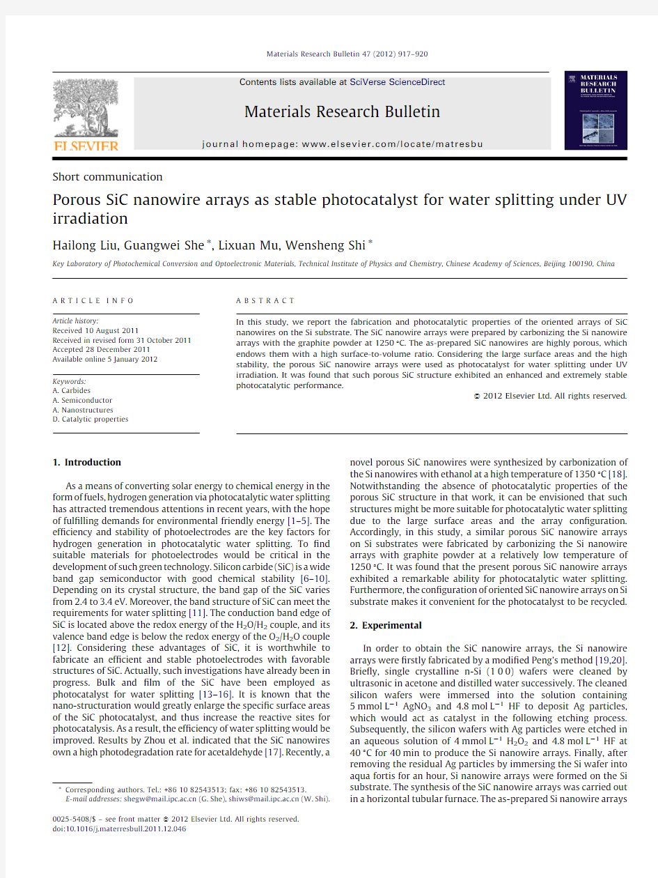
Fig.1a shows a schematic diagram of the equipment for the SiC nanowire arrays preparation.The silicon nanowire arrays were covered upon the graphite powder.The XRD characterization was utilized to con?rm the formation of the products,which results are shown in Fig.1b.In the XRD spectrum of the Si nanowire arrays (spectrum 1in Fig.1b),we can only observe two strong peaks locate at 33and 61.7degree,corresponding to the (200)plane and beta peak of the (400)plane of cubic Si respectively.After carbonization of the Si nanowire arrays with the graphite powder,except a weak peak at about 51.58from the residual carbon in the products,other three peaks can be readily indexed to that of cubic b -SiC (JCPDS No.29-1129).No diffraction peaks from Si were found,indicating that the Si was entirely converted to SiC.
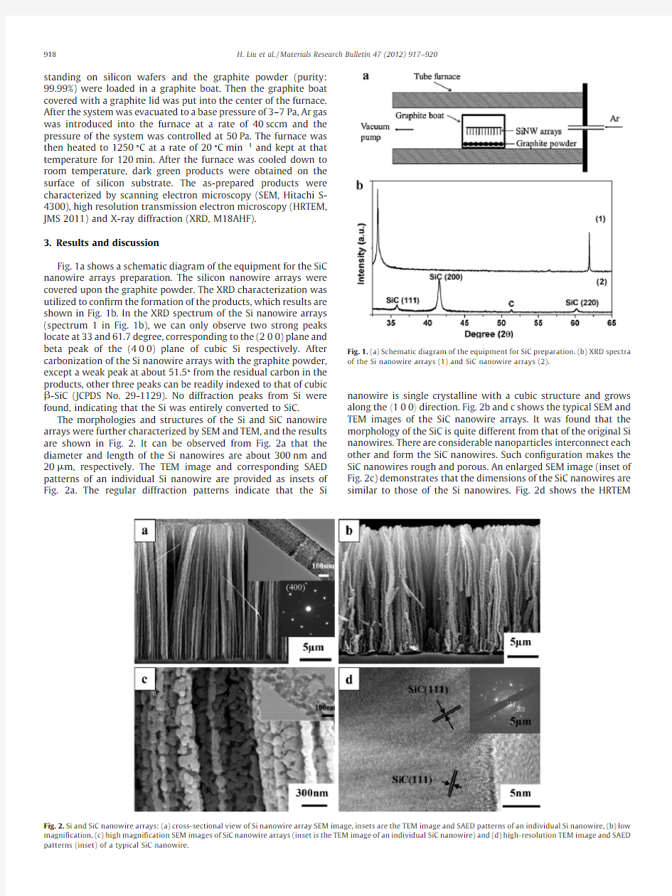
The morphologies and structures of the Si and SiC nanowire arrays were further characterized by SEM and TEM,and the results are shown in Fig.2.It can be observed from Fig.2a that the diameter and length of the Si nanowires are about 300nm and 20m m,respectively.The TEM image and corresponding SAED patterns of an individual Si nanowire are provided as insets of Fig.2a.The regular diffraction patterns indicate that the Si
nanowire is single crystalline with a cubic structure and grows along the h 100i direction.Fig.2b and c shows the typical SEM and TEM images of the SiC nanowire arrays.It was found that the morphology of the SiC is quite different from that of the original Si nanowires.There are considerable nanoparticles interconnect each other and form the SiC nanowires.Such con?guration makes the SiC nanowires rough and porous.An enlarged SEM image (inset of Fig.2c)demonstrates that the dimensions of the SiC nanowires are similar to those of the Si nanowires.Fig.2d shows the
HRTEM
Fig.1.(a)Schematic diagram of the equipment for SiC preparation.(b)XRD spectra of the Si nanowire arrays (1)and SiC nanowire arrays
(2).
Fig.2.Si and SiC nanowire arrays:(a)cross-sectional view of Si nanowire array SEM image,insets are the TEM image and SAED patterns of an individual Si nanowire,(b)low magni?cation,(c)high magni?cation SEM images of SiC nanowire arrays (inset is the TEM image of an individual SiC nanowire)and (d)high-resolution TEM image and SAED patterns (inset)of a typical SiC nanowire.
H.Liu et al./Materials Research Bulletin 47(2012)917–920
918
image and SAED patterns(inset)of the as-synthesized SiC nanowires.It reveals that the nanoparticles are polycrystalline. No Si phase was detected by the HRTEM,which further con?rms that the Si nanowires have been entirely converted to SiC nanowires.All the results illustrated that the Si nanowires not only provided as source for the formation of SiC,but also be used as a template to astrict the con?guration of the SiC.
The conversion from Si nanowires to SiC nanowires can be explained as follows.The graphite boat with graphite powder provided a carbon ambient at the temperature of12508C.In this case,the Si nanowires on Si substrates could be in situ carbonized. Due to the con?nement by the con?guration of the original Si nanowires,the one-dimensional SiC nanowires were formed.It is needed to indicate that a closed reaction condition is necessary since the low vapor pressure of the carbon at this temperature.It was found that the Si nanowires cannot be carbonized to form the SiC nanowires in an open system.This is why the graphite boat must be covered by a graphite lid during the whole reaction process.Accordingly,the carbon ambient is a crucial issue for the formation of SiC nanowires.
SiC nanomaterials have shown great potential in photocata-lytic applications[17].The porous structure provides the SiC nanowire arrays large speci?c areas,which may greatly enhance the photocatalytic performance.The photocatalytic activity of the as-synthesized b-SiC nanowires was evaluated by water splitting in a quartz vessel under UV irradiation.The experi-ments were carried out with a three-electrode electrochemical system.The SiC nanowire arrays on silicon substrates were used as the working electrode,an SCE electrode and platinum foil were used as reference and counter electrode,respectively.An aqueous solution containing0.3mol Là1KOH was used as the electrolyte.The electrochemical workstation(CHI600C)was used to scan the potential in linear sweep voltammetry at a rate of50mV sà1and monitor the current.In order to remove oxygen,the solution was continuously degassed with N2before and during the experiments.
The photocatalytic performance of the SiC nanowire arrays was examined under the darkness and irradiation of UV light(200W/ cm2)(Fig.3).The dark current density is as low as about10à3mA/ cm2at the bias potential fromà0.4V to1.0V(vs.SCE).However, the photocurrent is about1.2mA/cm2at the bias ofà0.2V(vs.SCE) and increased to22mA/cm2at the bias potential of1.0V(vs.SCE).
The photocurrent of the as-synthesized SiC nanowires is about 1000times higher than the dark current,demonstrating that the porous SiC nanowire arrays have a good ability to split water under the irradiation of UV light.It was found that our products own a higher ef?ciency than that of the reported bulk SiC at the same experimental conditions[13,15,16].Fig.3b shows the time dependence of the photocurrent and dark current of the as-synthesized SiC nanowires at the bias potential of0.0V(vs.SCE). The photocurrent is kept at2.2mA/cm2and the dark current is about10à3mA/cm2within120min.No decay of the photocurrent density was observed.It reveals that the as-synthesized SiC nanowires as photoelectrodes are very stable during the water splitting process.These results could be further con?rmed by the SEM observation on the electrode surface.There is no observable change on the morphology of the electrodes could be detected after the water splitting experiments.
Illuminating the SiC nanowire arrays would create electrons and holes.The holes could oxidize water to oxygen while the electrons would reduce protons or water to hydrogen at the Pt counter electrode.It is known that the photocatalytic activity of a semiconductor material strongly depends on its speci?c surface area.The as-synthesized SiC nanowires are consisted of inter-connected SiC nanocrystallites.Such con?guration provides larger speci?c surface area than that of the common SiC nanowires.Meanwhile,the nano-size SiC crystallites have small diameter.In this situation,the electrons can easily migrate from interior to outside of the SiC,which can ef?ciently reduce the recombination of the electron and hole and improve the ef?ciency of water splitting.Therefore,the as-synthesized SiC nanowires could exhibit good photocatalytic water splitting properties.
4.Conclusion
In summary,we developed a simple and effective method to fabricate highly oriented porous SiC nanowire arrays on silicon substrates by carbonization of the Si nanowire arrays.The SiC nanowires have the similar diameter and length of the original Si nanowires.The porous structure provides the SiC nanowire arrays a large speci?c surface area.Bene?tting from this virtue,the as-synthesized SiC nanowire arrays show good performance in photoelectrochemical water splitting.The highly oriented SiC porous nanowire arrays provide a potential application for hydrogen generation.
Acknowledgments
This work was supported by Chinese Academy of Sciences,NSFC (Grant Nos.21103211,10874189,50902134,and
61025003), Fig.3.(a)Linear sweep voltammetry of as-synthesized SiC nanowire arrays on Si substrate under the irradiation of UV light and darkness.(b)Current–time curve of as-synthesized SiC nanowire arrays under the irradiation of UV light and darkness.
H.Liu et al./Materials Research Bulletin47(2012)917–920919
National Basic Research Program of China(973Program)(Grant Nos.2010CB934103and2012CB932400)and Beijing Natural Science Foundation(Grant No.2102043).
References
[1]A.Fujishima,K.Honda,Nature238(1972)37.
[2]J.M.Ogden,Annu.Rev.Energy.Environ.24(1999)227.
[3]T.G.Deustch,C.A.Koval,J.A.Turner,J.Phys.Chem.B110(2006)25297.
[4]K.Maeda,T.Takata,M.Hara,N.Saito,Y.Inoue,H.Kobayashi,K.Domen,J.Am.
Chem.Soc.127(2005)8286.
[5]A.J.Nozik,R.Memming,J.Phys.Chem.100(1996)13061.
[6]H.Morkoc,S.Strite,G.B.Gao,M.E.Lin,B.Sverdlov,M.Bums,J.Appl.Phys.76
(1994)1363.
[7]P.G.Neudeck,J.Electron.Mater.24(1995)283.
[8]J.B.Casady,R.W.Johnson,Solid State Electron.39(1996)1409.
[9]G.Demir,T.E.Renfro,R.Glosser,S.E.Saddow,J.Appl.Phys.Lett.84(2004)3540.
[10]Q.Z.Zhao,F.Ciobanu,S.Malzer,L.Wang,J.Appl.Phys.Lett.91(2007)121107.
[11]R.Memming,Electrochim.Acta25(1980)77.
[12]C.H.Park,B.H.Cheong,K.H.Lee,K.Chang,J.Phys.Rev.B49(1994)4485.
[13]C.Schnabel,M.Worner,B.Gonzalez,I.Del Olmo,M.Braun,Electrochim.Acta.47
(2001)719.
[14]https://www.360docs.net/doc/ae5451870.html,rermann,R.Memming,D.Meissner,J.Electrochem.Soc.144(1997)73.
[15]J.Akikusa,S.U.M.Khan,Int.J.Hydrogen Energy27(2002)863.
[16]D.H.Van Dorp,N.Hijnen,M.D.Vece,J.J.Kelly,Angew.Chem.Int.Ed.48(2009)
6085.
[17]W.M.Zhou,L.J.Yan,Y.Wang,Y.F.Zhang,Appl.Phys.Lett.89(2006)013105.
[18]Y.J.Yang,G.W.Meng,X.Y.Liu,L.D.Zhang,Z.Hu,C.Y.He,Y.Hu,J.Phys.Chem.C112
(2008)20126.
[19]K.Q.Peng,Z.P.Huang,J.Zhu,Adv.Mater.16(2004)73.
[20]K.Q.Peng,Y.Xu,Y.Wu,Y.J.Yan,S.T.Lee,J.Zhu,Small1(2005)1062.
H.Liu et al./Materials Research Bulletin47(2012)917–920 920