AP2281-3WG-7;AP2281-3FMG-7;AP2281-1WG-7;中文规格书,Datasheet资料
Single Slew Rate Controlled Load Switch
? Wide input voltage range: 1.5V – 6V ? Low R DS(ON): 80m Ω typical @ 5V ? Turn-on slew rate controlled ? AP2281-1: 1ms turn-on rise time ? AP2281-3: 100us turn-on rise time with internal discharge ? Very low turn-on quiescent current: << 1uA ? Fast load discharge option ? Temperature range -40oC to 85°C ? SOT26 and DFN2018-6: Available in “Green” Molding
Compound (No Br, Sb) ? Lead Free Finish/ RoHS Compliant (Note 1)
The AP2281 slew rate controlled load switch is a single P-channel MOSFET power switch designed for high-side load-switching applications. The MOSFET has a typical R DS(ON) of 80m Ω at 5V, allowing increased load current handling capacity with a low forward voltage drop. The turn-on slew rate of the device is controlled internally.
The AP2281 load switch is designed to operate from 1.5V to 6V, making it ideal for 1.8V, 2.5V, 3.3V, and 5V systems. The typical quiescent supply current is only 0.01uA.
? Smart Phones ? PDA ? Cell Phones ? GPS Navigators ? PMP/MP4 ? Notebook and Pocket PC
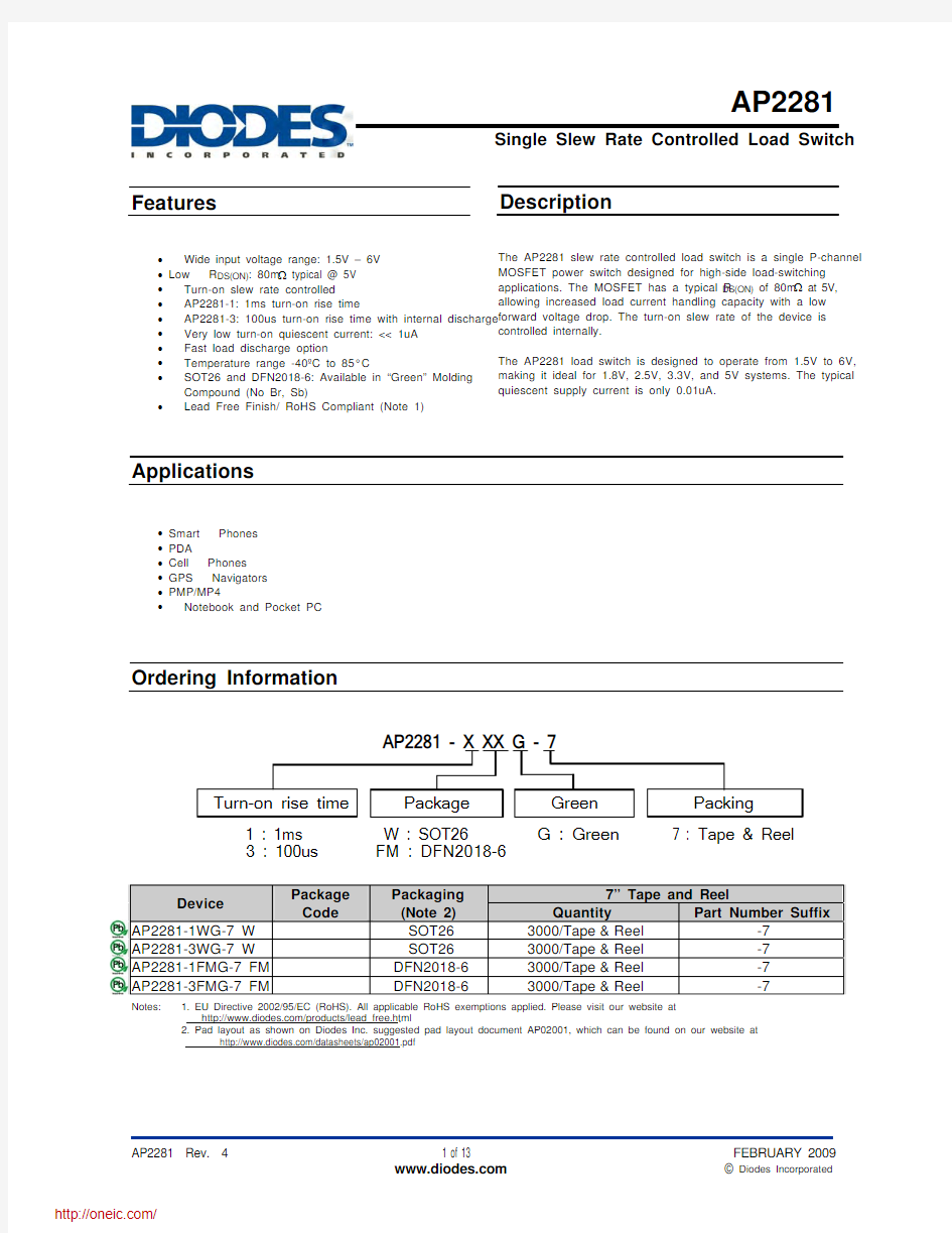
Package Packing 7 : Tape & Reel
Green G : Green
AP2281 - X XX G - 7
W : SOT26
Turn-on rise time
1 : 1ms 3 : 100us
FM : DFN2018-6
Device
Package Code Packaging
(Note 2) 7” Tape and Reel Quantity Part Number Suffix
AP2281-1WG-7 W SOT26 3000/Tape & Reel -7 AP2281-3WG-7 W SOT263000/Tape & Reel -7 AP2281-1FMG-7 FM DFN2018-6 3000/Tape & Reel -7 AP2281-3FMG-7 FM DFN2018-6 3000/Tape & Reel -7
Notes: 1. EU Directive 2002/95/EC (RoHS). All applicable RoHS exemptions applied. Please visit our website at https://www.360docs.net/doc/b01805973.html,/products/lead_free.html .
2. Pad layout as shown on Diodes Inc. suggested pad layout document AP02001, which can be found on our website at
https://www.360docs.net/doc/b01805973.html,/datasheets/ap02001.pdf
Features
Description
Applications
Ordering Information
Single Slew Rate Programmable Load Switch
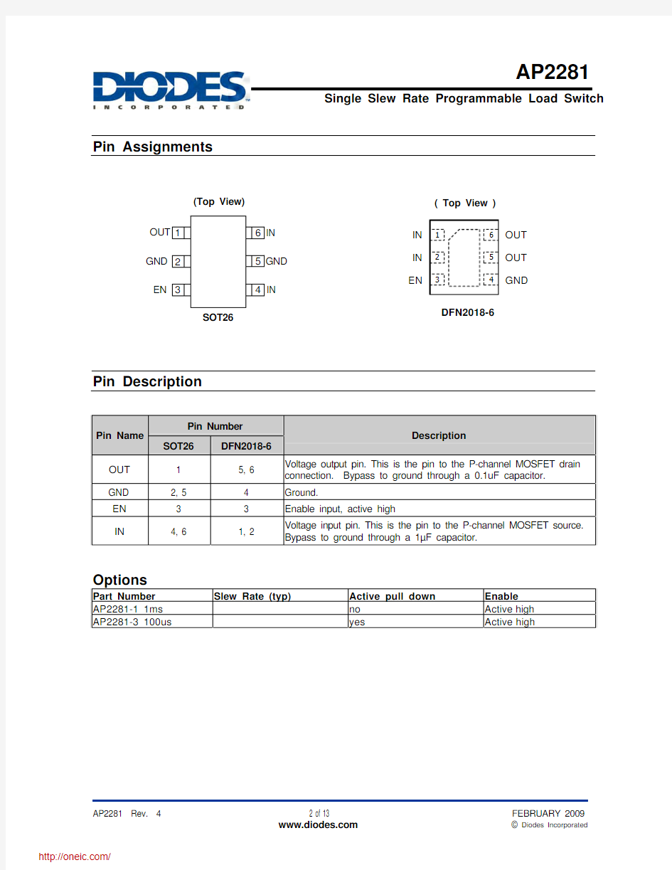
SOT26
GND EN (Top View)
IN IN EN
DFN2018-6
123
654
OUT OUT GND
( Top View )
Pin Name Pin Number Description
SOT26 DFN2018-6
OUT 1 5, 6 Voltage output pin. This is the pin to the P-channel MOSFET drain connection. Bypass to ground through a 0.1uF capacitor. GND 2, 5 4 Ground.
EN 3 3 Enable input, active high
IN
4, 6
1, 2
Voltage input pin. This is the pin to the P-channel MOSFET source. Bypass to ground through a 1μF capacitor.
Options
Part Number Slew Rate (typ) Active pull down Enable
AP2281-1 1ms no
Active high
AP2281-3 100us yes
Active high
Pin Assignments
Pin Description
Single Slew Rate Programmable Load Switch
Block Diagram
Typical Application Circuit
Single Slew Rate Programmable Load Switch Absolute Maximum Ratings
Symbol Parameter Ratings Unit
ESD HBM Human Body Model ESD Protection 5 KV
ESD MM Machine Model ESD Protection SOT26500 V DFN2018-6 450 V
V IN Input Voltage 6.5 V V OUT Output Voltage V IN + 0.3 V
V EN Enable Voltage 6.5 V I load Maximum Continuous Load Current 2 A T J Operating Junction Temperature Range-40 ~ 125 °C
T ST Storage Temperature Range-65 ~ 150 °C
P D Power Dissipation SOT26 (Note 3, 4, 5)720 mW DFN2018-6 (Note 3, 4, 6) 1410 mW
Notes: 3. T J, max =125°C.
4. Ratings apply to ambient temperature at 25°C.
Recommended Operating Conditions
Symbol Parameter Min Max Unit V IN Input voltage 1.5 6.0 V
I OUT Output Current 0 2.0 A
T A Operating Ambient Temperature -40 85 °C
Single Slew Rate Programmable Load Switch
(T A = 25o C, V IN= 5.0V, unless otherwise stated)
Symbol Parameters Test Conditions Min Typ. Max Unit
I Q Input Quiescent Current V EN = V IN, I OUT= 0 ?0.01 1 μA
I SHDN Input Shutdown Current V EN = 0V, OUT open ?0.01 1 μA
I LEAK Input Leakage Current V EN = 0V, OUT grounded ?0.01 1 μA
R DS(ON) Switch on-resistance V IN = 5.0V 80 100 m?V IN = 3.3V 95 120 m?V IN = 1.8V 160 210 m?V IN = 1.5V 210 280 m?
V IL EN Input Logic Low Voltage V IN = 1.5V to 6V 0.4 V
V IH EN Input Logic High Voltage 1.5V ≤ V IN≤ 2.7V 1.4 V
2.7V < V IN < 5.25V 1.6 V
V IN≥ 5.25V 1.7 V
I SINK EN Input leakage V EN = 5V ? 1 μA T D(ON)Output turn-on delay time R load=10Ω 1 μS
T ON Output turn-on rise time AP2281-1, R load=10Ω 1000 1500 μS AP2281-3, R load=10Ω 100 150 μS
T D(OFF) Output turn-off delay time R load=10Ω 0.5 1 μS R DISCH Discharge FET on-resistance For AP2281-3 only, V EN = GND 65 100 ?
θJA Thermal Resistance
Junction-to-Ambient
SOT26 (Note 5) 153
o C/W
DFN2018-6 (Note 6) 78
θJC Thermal Resistance
Junction-to-case
SOT26 (Note 5) 29
o C/W
DFN2018-6 (Note 6) 19
Notes: 5. Test condition for SOT26: Device mounted on FR-4 substrate PC board, 2oz copper, with minimum recommended pad layout.
6. Test condition for DFN2018-6: Device mounted on FR-4 2-layer board, 2oz copper, with minimum recommended pad on top layer and 3 vias to
bottom layer 1.0"x1.4" ground plane.
Electrical Characteristics
Single Slew Rate Programmable Load Switch
Typical Performance Characteristics
Single Slew Rate Programmable Load Switch
Typical Performance Characteristics (Continued)
AP2281-1 Turn-On (V IN=3.3V, R L=7?)
Time (500μs/div)AP2281-1 Turn-Off (V IN=3.3V, R L=7?)
Time (50μs/div)
AP2281-1 Turn-On (V IN=5V, R L=10?)
Time (500μs/div)AP2281-1 Turn-Off (V IN=5V, R L=10?)
Time (50μs/div)
V EN (5V/div)
V OUT (2V/div) I IN (500mA/div)V EN (5V/div) V OUT (2V/div) I IN (500mA/div)
V EN (5V/div)
V OUT (2V/div) I IN (500mA/div)V EN (5V/div)
V OUT (2V/div) I IN (500mA/div)
Single Slew Rate Programmable Load Switch
Typical Performance Characteristics (Continued)
AP2281-3 Turn-On (V IN=3.3V, R L=7?)
Time (50μs/div)AP2281-3 Turn-Off (V IN=3.3V, R L=7?)
Time (50μs/div)
AP2281-3 Turn-On (V IN=5V, R L=10?)
Time (50μs/div)AP2281-3 Turn-Off (V IN=5V, R L=10?)
Time (50μs/div)
V EN (5V/div)
V OUT (2V/div) I IN (500mA/div)V EN (5V/div) V OUT (2V/div) I IN (500mA/div)
V EN (5V/div)
V OUT (2V/div) I IN (500mA/div)V EN (5V/div)
V OUT (2V/div) I IN (500mA/div)
Single Slew Rate Programmable Load Switch
Input Capacitor
A 1μF capacitor is recommended to connect between IN and GND pins to decouple input power supply glitch and noise. The input capacitor has no specific type or ESR (Equivalent Series Resistance) requirement. However, for higher current application, ceramic capacitors are recommended due to their capability to withstand input current surges from low impedance sources, such as batteries in portable applications. This input capacitor must be located as close as possible to the device to assure input stability and less noise. For PC
B layout, a wide copper trace is required for both IN and GND.
Output Capacitor
A 0.1μF capacitor is recommended to connect between OUT and GND pins to stabilize and accommodate load transient condition. The output capacitor has no specific type or ESR requirement. The amount of the capacitance may be increased without limit. For PC
B layout, the output capacitor must be placed as close as possible to OUT and GND pins, and keep the traces as short as possible.
ENABLE/SHUTDOWN Operation
The AP2281 is turned on by setting the EN pin high, and is turned off by pulling it low. To ensure proper operation, the signal source used to drive the EN pin must be able to swing above and below the specified turn-on/off voltage thresholds listed in the Electrical Characteristics section under V IL and V IH.
DISCHARGE Operation
The AP2281-3 offers discharge option that helps to discharge the output charge when disabled. Power Dissipation
The device power dissipation and proper sizing of the thermal plane is critical to avoid thermal shutdown and ensure reliable operation. Power dissipation of the device depends on input voltage and load conditions and can be calculated by:
DSON
2
OUT
D
xR
I
P=(1)
However, the maximum power dissipation that can be handled by the device depends on the maximum junction to ambient thermal resistance, maximum ambient temperature, and maximum device junction temperature, which can be approximated by the equation below:
JA
A
A
D
)
T
C
125
(
)
T
(max@
P
θ
?
°
+
= (2)
For example at V IN = 5V, the typical R DSON = 80m?. For
I OUT = 2A, the maximum power dissipation calculated using equation (1) is P D = 0.32W. Based on SOT26 θJA = 153°C/W and equation (2), the calculated junction temperature rise from ambient is approximately 49°C. Since the maximum junction temperature is 125°C, the operating ambient temperature must be kept below 76°C
to safely operate the device.
On the other hand, at T A = 85°C and V IN = 5V, the calculated maximum power dissipation from equation (2)
is approximately P Dmax = 0.26W. Hence the safe operating maximum continuous current is 1.81A. For other application conditions, the users should recalculate the device maximum power dissipation based on the operating conditions.
Application Note
Single Slew Rate Programmable Load Switch
(1) SOT26
( Top View )
XX : Identification code W : Week : A~Z : 1~26 week;
X : A~Z : Green
Y : Year 0~9
a~z : 27~52 week; z represents 52 and 53 week
(2) DFN2018-6
( Top View )XX : Identification code W : Week : A~Z : 1~26 week;
X : A~Z : Green
Y : Year 0~9
a~z : 27~52 week; z represents 52 and 53 week
Marking Information
Device
Package type
Identification Code
AP2281-1W SOT26 U2 AP2281-3W SOT26
U3
Device
Package type
Identification Code
AP2281-1FM DFN2018-6 UE AP2281-3FM DFN2018-6
UF
分销商库存信息:
DIODES
AP2281-3WG-7AP2281-3FMG-7AP2281-1WG-7