MAAPGM0053-DIE中文资料
Amplifier, Distributed Power, 0.5 W
2.0-18.0 GHz
MAAPGM0053-DIE
903217 —
Preliminary Information
Features
? 0.5 Watt Saturated Output Power Level ? Variable Drain Voltage (5-10V) Operation ? MSAG? Process
?
Proven Manufacturability and Reliability
No Airbridges Polyimide Scratch Protection No Hydrogen Poisoning Susceptibility
Description
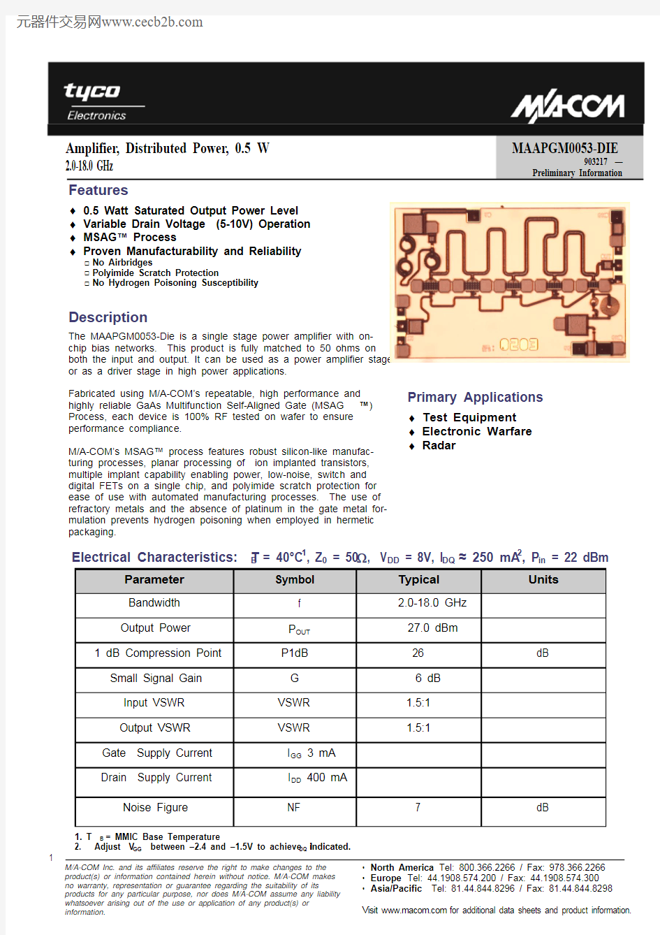
The MAAPGM0053-Die is a single stage power amplifier with on-chip bias networks. This product is fully matched to 50 ohms on both the input and output. It can be used as a power amplifier stage or as a driver stage in high power applications.
Fabricated using M/A-COM’s repeatable, high performance and highly reliable GaAs Multifunction Self-Aligned Gate (MSAG ?)Process, each device is 100% RF tested on wafer to ensure performance compliance.
M/A-COM’s MSAG? process features robust silicon-like manufac-turing processes, planar processing of ion implanted transistors, multiple implant capability enabling power, low-noise, switch and digital FETs on a single chip, and polyimide scratch protection for ease of use with automated manufacturing processes. The use of refractory metals and the absence of platinum in the gate metal for-mulation prevents hydrogen poisoning when employed in hermetic packaging.
Parameter Symbol
Typical
Units
Bandwidth f 2.0-18.0 GHz Output Power P OUT 27.0 dBm 1 dB Compression Point P1dB 26
dB
Small Signal Gain G 6 dB Input VSWR VSWR 1.5:1 Output VSWR VSWR
1.5:1
Gate Supply Current I GG 3 mA Drain Supply Current
I DD 400 mA Noise Figure
NF
7
dB
1. T B = MMIC Base Temperature
2. Adjust V GG between –2.4 and –1.5V to achieve I DQ indicated. Electrical Characteristics: T B = 40°C 1, Z 0 = 50Ω, V DD = 8V, I DQ ≈ 250 mA 2, P in = 22 dBm
Primary Applications
? Test Equipment ? Electronic Warfare ? Radar
Amplifier, Distributed Power, 0.5 W
2.0-18.0 GHz
MAAPGM0053-DIE
903217 —
Preliminary Information
Characteristic Symbol
Min
Typ
Max
Unit
Drain Supply Voltage V DD 5.0 8.0 10.0 V Gate Supply Voltage
V GG -2.4 -2.0 -1.5 V Input Power P IN 22.0 24.0 dBm Junction Temperature T J 150 °C MMIC Base Temperature
T B
Note 4
°C
Thermal Resistance ΘJC 19.6 °C/W Maximum Operating Conditions 3
Operating Instructions
This device is static sensitive. Please handle with care. To operate the device, follow these steps.
1. Apply V GG = -2 V, V DD = 0 V.
2. Ramp V DD to desired voltage, typically 8 V.
3. Adjust V GG to set I DQ .
4. Set RF input.
5. Power down sequence in reverse. Turn V GG off last.
Recommended Operating Conditions
Parameter Symbol
Absolute Maximum
Units Input Power P IN 25.0 dBm Drain Supply Voltage V DD +12.0 V Gate Supply Voltage
V GG -3.0 V Quiescent Drain Current (No RF, 40% Idss) I DQ 400 mA Quiescent DC Power Dissipated (No RF)
P DISS 4.0 W Junction Temperature T J 180 °C Storage Temperature T STG
-55 to +150
°C Die Attach Temperature
310
°C
3. Operation outside of these ranges may reduce product reliability. Operation at other than the typical values may result in performance outside the guaranteed limits.
4. Maximum MMIC Base Temperature = 150°C —ΘJC * V DD * I DQ
Amplifier, Distributed Power, 0.5 W
2.0-18.0 GHz
MAAPGM0053-DIE
903217 —
Preliminary Information
2
3
4
5
6
7
8
9
10
11
12
13
14
15
16
17
18
Frequency (GHz)
P o w e r O u t (d B m )
D r a i n C u r r e n t (A )
Power Out Drain Current
Figure 1. Output Power and Drain Current at P in = 22 dBm and V DD = 8V.
Figure 2: Small Signal Gain and VSWR at V D =5V
2
3
4
5
6
7
8
9
10
11
12
13
14
15
16
17
18
19
20
Frequency (GHz)
G a i n (d B )
V S W R Gain
Input VSWR Output VSWR
10
11
12
13
14
15
16
17
18
19
20
21
22
23
24
25
Power In (dBm)
P o w e r O u t (d B m )
0.10
0.140.180.220.260.300.340.38
0.420.460.50D r a i n C u r r e n t (A )
Po @ 2GHz Po @ 6GHz Po @ 10GHz Po @ 14GHz Po @ 18GHz Ids @ 2GHz
Ids @ 6GHz
Ids @ 10GHz
Ids @ 14GHz
Ids @ 18GHz
Figure 3. Output Power and Drain Current vs. Input Power at V DD = 5V.
1012141618202224
26283010
11
12
13
14
15
16
17
18
19
20
21
22
23
24
25
Power In (dBm)
P o w e r O u t (d B m )
D r a i n C u r r e n t (A )
Po @ 2GHz Po @ 6GHz Po @ 10GHz Po @ 14GHz Po @ 18GHz Ids @ 2GHz
Ids @ 6GHz
Ids @ 10GHz
Ids @ 14GHz
Ids @ 18GHz
Figure 4. Output Power and Drain Current vs. Input Power at V DD = 8V.
1012141618202224
26283010
11
12
13
14
15
16
17
18
19
20
21
22
23
24
25
Power In (dBm)P o w e r O u t (d B m )
0.10
0.140.18
0.220.260.300.340.380.420.460.50D r a i n C u r r e n t (A )
Po @ 2GHz Po @ 6GHz Po @ 10GHz Po @ 14GHz Po @ 18GHz Ids @ 2GHz
Ids @ 6GHz
Ids @ 10GHz
Ids @ 14GHz
Ids @ 18GHz
Figure 5. Output Power and Drain Current vs. Input Power at V DD = 10V.
15
16
17
18
19
20
21
22
23
24
25
26
27
28
29
30
Power Out (dBm)
G a i n (d B )
Gain @ 2GHz Gain @ 6GHz Gain @ 10GHz Gain @ 14GHz Gain @ 18GHz
Figure 6. Compression Characteritics, Gain vs Power Out at V DD = 8V.
Amplifier, Distributed Power, 0.5 W
2.0-18.0 GHz MAAPGM0053-DIE
903217 —
Preliminary Information
Mechanical Information
Chip Size: 3.000 x 2.000 x 0.075 mm (118 x 79 x 3 mils)
Pad Size (μm) RF In and Out
100 x 150 DC Drain Supply Voltage VDD 150 x 150 DC Gate Supply Voltage VGG
150 x 150
Size (mils) 4 x 8 8 x 6 4 x 6
Bond Pad Dimensions
Chip edge to bond pad dimensions are shown to the center of the bond pad.
Figure 7. Die Layout
0.467mm 0
1.838mm
0.177mm
2.843mm
3.000mm
1.216mm
1.042mm
2.341mm
GND:G
VG GND:D
GND:G
GND:G
GND:G
OUT
VD
GND:D
IN
0.137mm
2.000mm
Amplifier, Distributed Power, 0.5 W
2.0-18.0 GHz MAAPGM0053-DIE
903217 —
Preliminary Information
Assembly Instructions:
Die attach: Use AuSn (80/20) 1 mil. preform solder. Limit time @ 300 °C to less than 5 minutes.
Wirebonding: Bond @ 160 °C using standard ball or thermal compression wedge bond techniques. For DC pad connections, use either ball or wedge bonds. For best RF performance, use wedge bonds of shortest length, although ball bonds are also acceptable.
Biasing Note: Must apply negative bias to V GG before applying positive bias to V DD to prevent damage to amplifier.
Figure 6. Recommended bonding diagram for pedestal mount.
Support circuitry typical of MMIC characterization fixture for CW testing.
100 pF
100 pF
RF IN
RF OUT
0.1 μF
V GG
0.1 μF
V DD
GND:G
VG GND:D
GND:G
GND:G
GND:G
OUT
VD
GND:D
IN
Assembly and Bonding Diagram