04N03LA
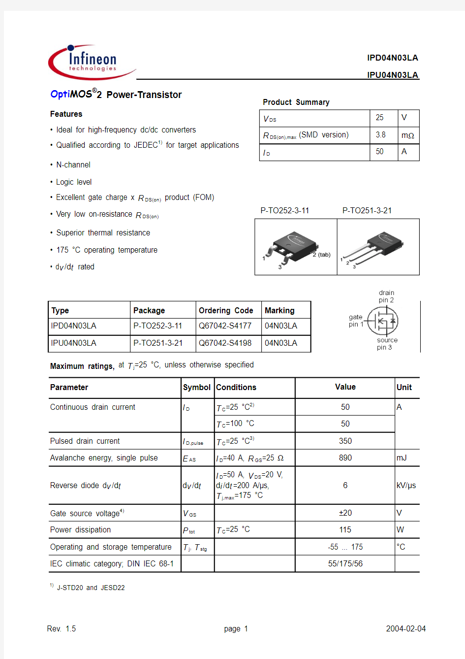
IPU04N03LA
Parameter
Symbol Conditions
Unit
min.
typ.
max.
Thermal characteristics
Thermal resistance, junction - case R thJC -- 1.3K/W
SMD version, device on PCB
R thJA
minimal footprint --756 cm 2 cooling area 5)
--50
Electrical characteristics, at T j =25 °C, unless otherwise specified Static characteristics
Drain-source breakdown voltage V (BR)DSS V GS =0 V, I D =1 mA 25--V
Gate threshold voltage V GS(th)V DS =V GS , I D =80 μA 1.2 1.62Zero gate voltage drain current
I DSS
V DS =25 V, V GS =0 V, T j =25 °C
-0.1
1
μA V DS =25 V, V GS =0 V, T j =125 °C
-10100Gate-source leakage current I GSS V GS =20 V, V DS =0 V -10100nA Drain-source on-state resistance
R DS(on)
V GS =4.5 V, I D =50 A - 4.8 5.9m ?
V GS =4.5 V, I D =50 A, SMD version - 4.6 5.7V GS =10 V, I D =50 A - 3.4 4.0V GS =10 V, I D =50 A, SMD version
- 3.2 3.8Gate resistance R G - 1.3-?Transconductance
g fs
|V DS |>2|I D |R DS(on)max , I D =50 A
48
96
-S 5)
Device on 40 mm x 40 mm x 1.5 mm epoxy PCB FR4 with 6 cm 2 (one layer, 70 μm thick) copper area for drain connection. PCB is vertical in still air.
Values 2)
Current is limited by bondwire; with an R thJC =1.3 K/W the chip is able to carry 136 A.3) See figure 3
4) T j,max =150 °C and duty cycle D <0.25 for V GS <-5 V
IPU04N03LA Parameter Symbol Conditions Unit
min.typ.max. Dynamic characteristics
Input capacitance C iss-39095199pF Output capacitance C oss-14881979 Reverse transfer capacitance C rss-174261
Turn-on delay time t d(on)-1421ns Rise time t r-1116
Turn-off delay time t d(off)-4466
Fall time t f- 6.610
Gate Charge Characteristics6)
Gate to source charge Q gs-1216nC Gate charge at threshold Q g(th)- 6.38.3
Gate to drain charge Q gd-8.112 Switching charge Q sw-1419
Gate charge total Q g-3141
Gate plateau voltage V plateau- 3.0-V
Gate charge total, sync. FET Q g(sync)V DS=0.1 V,
V GS=0 to 5 V
-2837nC
Output charge Q oss V DD=15 V, V GS=0 V-3243 Reverse Diode
Diode continous forward current I S--50A Diode pulse current I S,pulse--350
Diode forward voltage V SD V GS=0 V, I F=50 A,
T j=25 °C
-0.89 1.2V
Reverse recovery charge Q rr V R=15 V, I F=I S,
d i F/d t=400 A/μs
--15nC
6) See figure 16 for gate charge parameter definition T C=25 °C
Values
V GS=0 V, V DS=15 V,
f=1 MHz
V DD=15 V, V GS=10 V,
I D=25 A, R G=2.7 ?
V DD=15 V, I D=25 A,
V GS=0 to 5 V
IPU04N03LA Package Outline
P-TO252-3-11: Outline
Footprint:Packaging:
Dimensions in mm
IPU04N03LA Package Outline
P-TO251-3-21: Outline
Dimensions in inch [mm]
IPU04N03LA Published by
Infineon Technologies AG
Bereich Kommunikation
St.-Martin-Stra?e 53
D-81541 München
? Infineon Technologies AG 1999
All Rights Reserved.
Attention please!
The information herein is given to describe certain components and shall not be considered as
warranted characteristics.
Terms of delivery and rights to technical change reserved.
We hereby disclaim any and all warranties, including but not limited to warranties of non-infringement, regarding circuits, descriptions and charts started herein.
Infineon Technologies is an approved CECC manufacturer.
Information
For further information on technology, delivery terms and conditions and prices, please contact your nearest Infineon Technologies office in Germany or our Infineon Technologies representatives worldwide (see address list).
Warnings
Due to technical requirements, components may contain dangerous substances.
For information on the types in question, please contact your nearest Infineon Technologies office. Infineon Technologies' components may only be used in life-support devices or systems with the expressed written approval of Infineon Technologies if a failure of such components can reasonably
be expected to cause the failure of that life-support device or system, or to affect the safety or effectiveness of that device or system. Life support devices or systems are intended to be implanted
in the human body, or to support and/or maintain and sustain and/or protect human life. If they fail,
it is reasonable to assume that the health of the user or other persons may be endangered.