SF1197B;中文规格书,Datasheet资料
Electrical Characteristics
Characteristic
Sym Notes Min
Typ Max Units Nominal Center Frequency f N 1
248.6MHz Minimal insertion attenuation a_min
3.04
dB 3 dB Band Width
5.0
6.5MHz Amplitude ripple (p - p) [fn ±120 kHz]0.3
0.5dB Group Delay ripple (p - p) [fn ±120 kHz]0.3μs
Relative attenuation (relative to amin)a_rel
10 MHz ....
(fn - 29,2 MHz)45.050dB fn + 22,8 MHz 45.050dB fn + 52,0 MHz 45.050dB fn + 74,8 MHz 45.050dB fn + 104,0 MHz 45.050dB fn + 126,8 MHz
45.0
50
dB
Case Style
SMP-03 7 X 5 mm Nominal Footprint
Lid Symbolization (Y=year, WW=week, S=shift) See note 3
RFM SF1197B YWWS
?Small Size
?Hermetic 7 X 5 mm Surface Mount Case ?No Matching Required
Input power Level
max. 20 dBm for <= 100 hours max. 10 dBm for <= 15 years Input: unsymmetrical Output: symmetrical Terminating source impedance:Zs = 50 Ohm (no matching network)Terminating load impedance:ZI = 200 Ohm (no matching network)
Low-Impedance Input: near 50 Ohm Low-Impedance Output: near 200 Ohm Operating Temperature
T = -20 to 80 [°C]
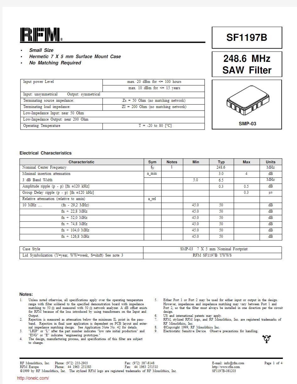
248.6 MHz SAW Filter
SF1197B 1.
Unless noted otherwise, all specifications apply over the operating temperature range with filter soldered to the specified demonstration board with impedance
matching to 50 ? and measured with 50 ? network analyzer. A dB offset exists
for RFM because of the loss introduced by using transformers on the Input and Output.2.Rejection is measured as attenuation below the minimum IL point in the pass-band. Rejection in final user application is dependent on PCB layout and exter-nal impedance matching design. See Application Note No. 42 for details.3."LRIP" or "L" after the part number indicates "low rate initial production" and
"ENG" or "E" indicates "engineering prototypes."
4.
The design, manufacturing process, and specifications of this filter are subject to change.
5.Either Port 1 or Port 2 may be used for either input or output in the design.
However, impedances and impedance matching may vary between Port 1 and Port 2, so that the filter must always be installed in one direction per the circuit https://www.360docs.net/doc/c29012933.html, and international patents may apply.
7.RFM, stylized RFM logo, and RF Monolithics, Inc. are registered trademarks of RF Monolithics, Inc.
8.?Copyright 1999, RF Monolithics Inc.
9.Electrostatic Sensitive Device. Observe precautions for handling.Notes:
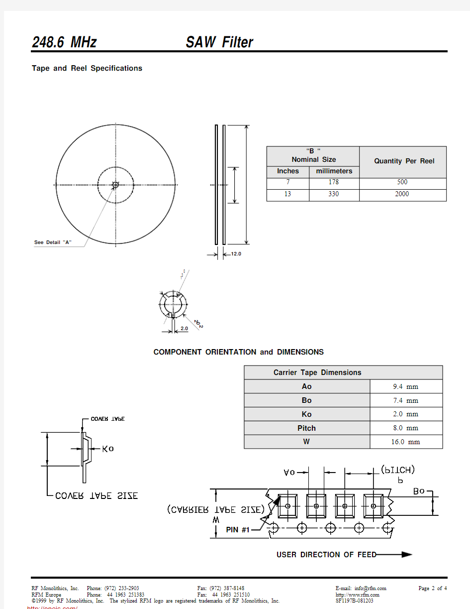
Tape and Reel Specifications
“B “
Nominal Size Quantity Per Reel
Inches
millimeters
717850013
330
2000
USER DIRECTION OF FEED
COMPONENT ORIENTATION and DIMENSIONS
Carrier Tape Dimensions
Ao 9.4 mm Bo 7.4 mm Ko 2.0 mm Pitch 8.0 mm W
16.0 mm
PIN #1
Dimension
mm Inches Min Nom Max Min Nom Max A 6.807.007.200.2680.2760.283B 4.80
5.00 5.200.189
0.1970.205C 1.65 2.00
0.0650.079
D 0.600.024
E 2.540.100H 1.00.039J 5.000.197K 3.000.118P
1.27
0.050
Connection
Terminals
Port 1Input or Return 10Return or Input 1Port 2
Output or Return 5Return or Output 6Ground
All others Single Ended Operation Return is ground Differential Operation
Return is hot
10-Terminal Ceramic Surface-Mount Case
7 x 5 mm Nominal Footprint
SMP-03 Case
Electrical Connections
Case Dimensions
Solder Temperature Profile
Figure 1 shows the recommended temperature profile for reflow soldering SMP-03 and SMP53-S package consists of a ceramic base with a metal lid that is attached with high-temperature solde age is hermetically sealed and the solder seal must not be compromised with excessive heat in a ical that the filter package is never heated above 250°C. It is recommended that the package b than 240°C for no more than 10 seconds.
分销商库存信息: RFM
SF1197B