MPS6521RLRAG中文资料
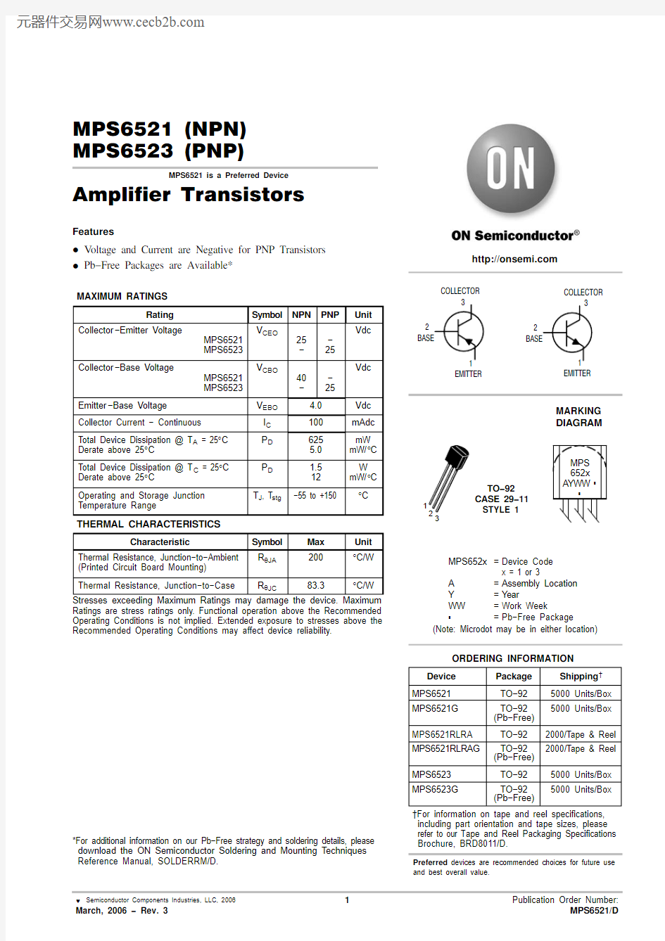
MPS6521 (NPN)
MPS6523 (PNP)
MPS6521 is a Preferred Device Amplifier Transistors
Features
?V oltage and Current are Negative for PNP Transistors
?Pb?Free Packages are Available*
MAXIMUM RATINGS
Rating Symbol NPN PNP Unit
Collector?Emitter Voltage
MPS6521
MPS6523V CEO
25
?
?
25
Vdc
Collector?Base Voltage
MPS6521
MPS6523V CBO
40
?
?
25
Vdc
Emitter
?Base Voltage V EBO 4.0Vdc
Collector Current ? Continuous I C100mAdc
Total Device Dissipation @ T A = 25°C Derate above 25°C P D625
5.0
mW
mW/°C
Total Device Dissipation @ T C = 25°C Derate above 25°C P D 1.5
12
W
mW/°C
Operating and Storage Junction
Temperature Range
T J, T stg?55 to +150°C THERMAL CHARACTERISTICS
Characteristic Symbol Max Unit
Thermal Resistance, Junction?to?Ambient (Printed Circuit Board Mounting)R
q JA200°C/W
Thermal Resistance, Junction?to?Case R q JC83.3°C/W Stresses exceeding Maximum Ratings may damage the device. Maximum Ratings are stress ratings only. Functional operation above the Recommended Operating Conditions is not implied. Extended exposure to stresses above the Recommended Operating Conditions may affect device reliability.
*For additional information on our Pb?Free strategy and soldering details, please download the ON Semiconductor Soldering and Mounting Techniques Reference Manual, SOLDERRM/D.
https://www.360docs.net/doc/c19170208.html,
?For information on tape and reel specifications, including part orientation and tape sizes, please refer to our T ape and Reel Packaging Specifications Brochure, BRD8011/D.
MPS6521RLRA TO?922000/Tape & Reel MPS6521RLRAG TO?92
(Pb?Free)
2000/Tape & Reel Device Package Shipping?MPS6521TO?925000 Units/Box MPS6521G TO?92
(Pb?Free)
5000 Units/Box
Preferred devices are recommended choices for future use and best overall value.
ORDERING INFORMATION
MPS6523TO?925000 Units/Box MPS6523G TO?92
(Pb?Free)
5000 Units/Box
ELECTRICAL CHARACTERISTICS (T A = 25°C unless otherwise noted)
Characteristic
Symbol
Min
Max
Unit
OFF CHARACTERISTICS
Collector ?Emitter Breakdown Voltage
(I C = 0.5 mAdc, I B = 0)V (BR)CEO 25?Vdc Emitter ?Base Breakdown Voltage
(I E = 10 m Adc, I C = 0)V (BR)EBO 4.0
?
Vdc Collector Cutoff Current
(V CB = 30 Vdc, I E = 0)MPS6521(V CB = 20 Vdc, I E = 0)MPS6523
I CBO
??0.050.05
m Adc
ON CHARACTERISTICS
DC Current Gain
(I C = 100 m Adc, V CE = 10 Vdc)
MPS6521(I C = 2.0 mAdc, V CE = 10 Vdc)MPS6521(I C = 100 m Adc, V CE = 10 Vdc)MPS6523(I C = 2.0 mAdc, V CE = 10 Vdc)MPS6523
h FE
150300150300?600?600?
Collector ?Emitter Saturation Voltage
(I C = 50 mAdc, I B = 5.0 mAdc)V CE(sat)?
0.5
Vdc
SMALL?SIGNAL CHARACTERISTICS Output Capacitance
(V CB = 10 Vdc, I E = 0, f = 1.0 MHz)
C obo ? 3.5pF Noise Figure
(I C = 10 m Adc, V CE = 5.0 Vdc, R S = 10 k W ,
Power Bandwidth = 15.7 kHz, 3.0 dB points @ 10 Hz and 10 kHz)
NF
?
3.0
dB
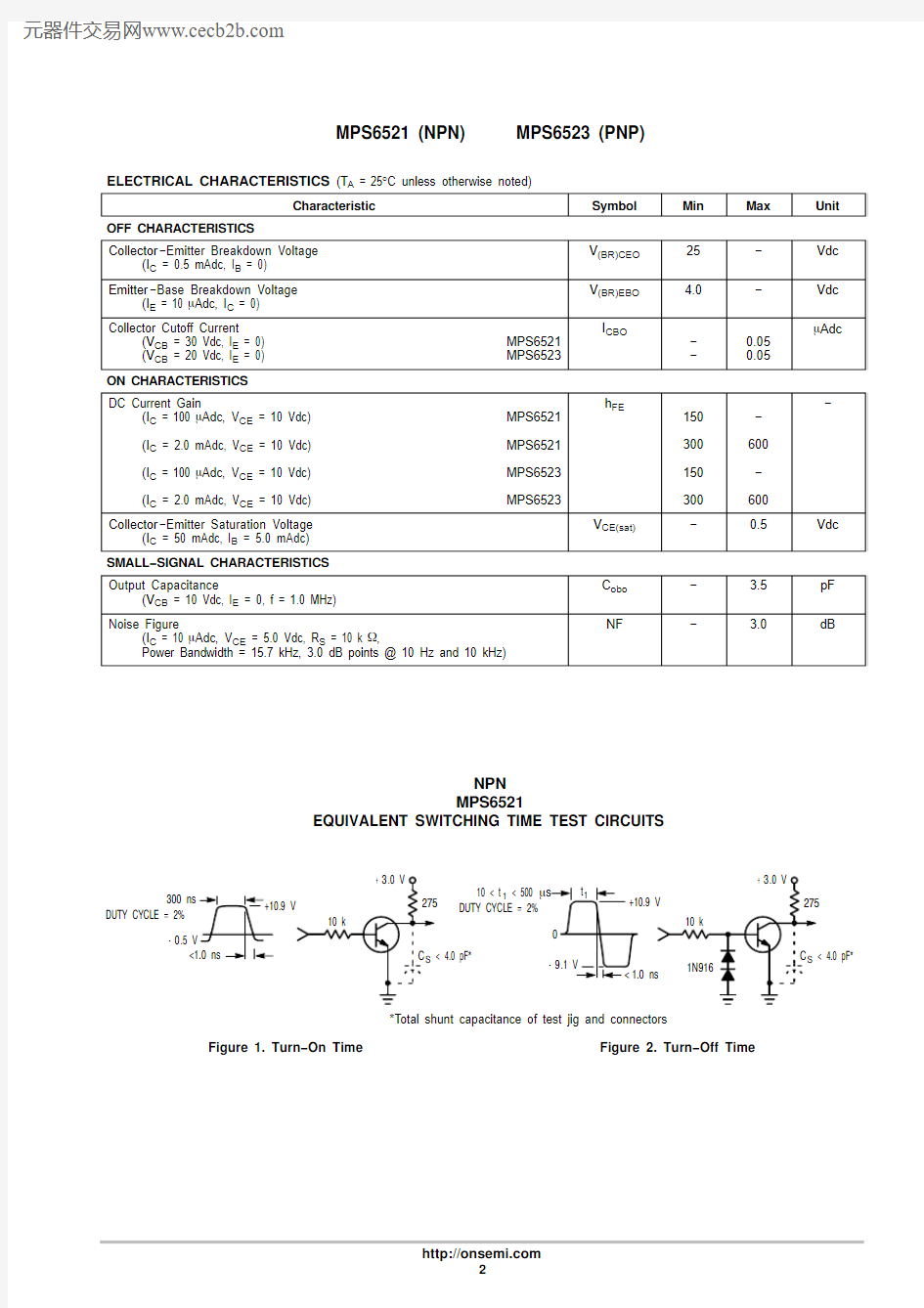
Figure 1. Turn?On Time Figure 2. Turn?Off Time
NPN MPS6521
EQUIVALENT SWITCHING TIME TEST CIRCUITS
*Total shunt capacitance of test jig and connectors
? 0
TYPICAL NOISE CHARACTERISTICS
(V CE = 5.0 Vdc, T A = 25°C)
Figure 3. Noise Voltage f, FREQUENCY (Hz)
5.0
7.01020
3.0Figure
4. Noise Current
f, FREQUENCY (Hz)
2.0
10
20
50
1002005001 k 2 k
5 k
10 k
e n , N O I S E V O L T A G E (n V )
10
20
501002005001 k 2 k
5 k
10 k
NPN MPS6521
NOISE FIGURE CONTOURS
(V CE = 5.0 Vdc, T A = 25°C)
500 k R S , S O U R C E R E S I S T A N C E (O H M S )
Figure 7. Wideband
I C , COLLECTOR CURRENT (m A)
10
R S , S O U R C E R E S I S T A N C E (O H M S )
50
1002005001 k 10 k 5 k 20 k 50 k 100 k 200 k 2 k 500 k 50
1002005001 k 10 k 5 k 20 k 50 k 100 k 200 k 2 k 20
30
5070100
200300
500700
1 k
NPN MPS6521
TYPICAL STATIC CHARACTERISTICS
h , D C C U R R E N T G A I N
F E I C , COLLECTOR CURRENT (mA)
1.4I C , COLLECTOR CURRENT (mA)
V , V O L T A G E (V O L T S )
Figure 11. “On” Voltages 0.40.60.81.00.2
V C E , C O L L E C T O R ?E M I T T E R V O L T A G E (V O L T S )
Figure 12. Temperature Coefficients
1.21.00.80.60.40.20
NPN MPS6521
TYPICAL DYNAMIC CHARACTERISTICS
300Figure 17. Input Impedance I C , COLLECTOR CURRENT (mA)
Figure 18. Output Admittance
I C , COLLECTOR CURRENT (mA)
500
t , T I M E (n s )
f , C U R R E N T ?G A I N B A N D W I D T H P R O D U C T (M H z )
T h i e , I N P U T I M P E D A N C E (k )
Ω 3.05.07.0102030507010020050
70
100200
300 2.0 5.010
20501.00.21000.30.50.71.02.03.05.07.010200.1
0.2
0.5
2.0 5.010
20501.0100
0.1
0.20.5
NPN MPS6521
Figure 19. Thermal Response
t, TIME (ms)
1.00.01r (t ) T R A N S I E N T T H E R M A L R E S I S T A N C E (N O R M A L I Z E D )
0.01
0.02
0.030.050.070.10.20.30.50.70.02
0.05
0.1
0.2
0.5
1.0
2.0
5.0
10
20
50
100200500 1.0 k 2.0 k
5.0 k 10 k 20 k 50 k 100 k
Figure 21.
T J , JUNCTION TEMPERATURE (°C)
104
0I C , C O L L E C T O R C U R R E N T (n A )
Figure 22.
V CE , COLLECTOR?EMITTER VOLTAGE (VOLTS)
400
I C , C O L L E C T O R C U R R E N T (m A )
DESIGN NOTE: USE OF THERMAL RESPONSE DATA
A train of periodical power pulses can be represented by the model as shown in Figure 20. Using the model and the device thermal response the normalized effective transient thermal resistance of Figure 19 was calculated for various duty cycles.To find Z q JA(t), multiply the value obtained from Figure 19 by the steady state value R q JA .Example:
The MPS6521 is dissipating 2.0 watts peak under the following conditions:
t 1 = 1.0 ms, t 2 = 5.0 ms. (D = 0.2)
Using Figure 19 at a pulse width of 1.0 ms and D = 0.2,the reading of r(t) is 0.22.
The peak rise in junction temperature is therefore D T = r(t) x P (pk) x R q JA = 0.22 x 2.0 x 200 = 88°C.For more information, see ON Semiconductor Application Note AN569/D, available from the Literature Distribution Center or on our website at https://www.360docs.net/doc/c19170208.html, .
The safe operating area curves indicate I C ?V CE limits of the transistor that must be observed for reliable operation. Collector load lines for specific circuits must fall below the limits indicated by the applicable curve.The data of Figure 22 is based upon T J(pk) = 150°C;T C or T A is variable depending upon conditions. Pulse curves are valid for duty cycles to 10% provided T J(pk)≤ 150°C. T J(pk) may be calculated from the data in Figure 19. At high case or ambient temperatures,thermal limitations will reduce the power that can be handled to values less than the limitations imposed by second breakdown.
10?2
10?11001011021030
4.06.010204060100200
PNP MPS6523
TYPICAL NOISE CHARACTERISTICS
(V CE = ?5.0 Vdc, T A = 25°C)
Figure 23. Noise Voltage f, FREQUENCY (Hz)
5.0
7.0103.0Figure 24. Noise Current
f, FREQUENCY (Hz)
1.0
102050
100200500 1.0 k 2.0 k 5.0 k 10 k
e n , N O I S E V O L T A G E (n V )
10
20
50
100200500 1.0 k 2.0 k 5.0 k
10 k
2.0
NOISE FIGURE CONTOURS
(V CE = ?5.0 Vdc, T A = 25°C)
500 k 100
2005001.0 k 10 k 5.0 k 20 k 50 k 100 k 200 k 2.0 k 1.0 M 500 k 100
2005001.0 k 10 k 5.0 k 20 k 50 k 100 k 200 k 2.0 k 1.0 M
R S , S O U R C E R E S I S T A N C E (O H M S )
Figure 27. Wideband
I C , COLLECTOR CURRENT (m A)
10
R S , S O U R C E R E S I S T A N C E (O H M S )
20
30
5070100
200300
500700 1.0 k
PNP MPS6523
TYPICAL STATIC CHARACTERISTICS
h , D C C U R R E N T G A I N
F E I C , COLLECTOR CURRENT (mA)
1.4I C , COLLECTOR CURRENT (mA)
V , V O L T A G E (V O L T S )
Figure 31. “On” Voltages 0.40.60.81.00.2
V C E , C O L L E C T O R ?E M I T T E R V O L T A G E (V O L T S )
Figure 32. Temperature Coefficients
1.21.00.80.60.40.20
PNP MPS6523
TYPICAL DYNAMIC CHARACTERISTICS
500Figure 37. Input Impedance I C , COLLECTOR CURRENT (mA)
Figure 38. Output Admittance
I C , COLLECTOR CURRENT (mA)
500
t , T I M E (n s )
f , C U R R E N T ?G A I N ? B A N D W I D T H P R O D U C T (M H z )
T h i e , I N P U T I M P E D A N C E (k )
Ω 5.07.0102030507010030050
70
100200
300 2.0 5.010
20501.00.21000.30.50.71.02.03.05.07.010200.1
0.2
0.5 2.0 5.010
20501.0100
0.1
0.20.5
200
PNP MPS6523
Figure 39. Thermal Response
t, TIME (ms)
1.00.01r (t ) T R A N S I E N T T H E R M A L R E S I S T A N C E (N O R M A L I Z E D )
0.01
0.02
0.030.050.070.10.20.30.50.70.02
0.05
0.1
0.2
0.5
1.0
2.0
5.0
10
20
50
100200500 1.0 k 2.0 k
5.0 k 10 k 20 k 50 k 100 k
Figure 41.
T J , JUNCTION TEMPERATURE (°C)
104?40I C , C O L L E C T O R C U R R E N T (n A )
Figure 42.
V CE , COLLECTOR?EMITTER VOLTAGE (VOLTS)
4002.0
I C , C O L L E C T O R C U R R E N T (m A )
DESIGN NOTE: USE OF THERMAL RESPONSE DATA
A train of periodical power pulses can be represented by the model as shown in Figure 40. Using the model and the device thermal response the normalized effective transient thermal resistance of Figure 39 was calculated for various duty cycles.To find Z q JA(t), multiply the value obtained from Figure 39 by the steady state value R q JA .Example:
The MPS6523 is dissipating 2.0 watts peak under the following conditions:
t 1 = 1.0 ms, t 2 = 5.0 ms. (D = 0.2)
Using Figure 39 at a pulse width of 1.0 ms and D = 0.2,the reading of r(t) is 0.22.
The peak rise in junction temperature is therefore D T = r(t) x P (pk) x R q JA = 0.22 x 2.0 x 200 = 88°C.For more information, see ON Semiconductor Application Note AN569/D, available from the Literature Distribution Center or on our website at https://www.360docs.net/doc/c19170208.html, .
The safe operating area curves indicate I C ?V CE limits of the transistor that must be observed for reliable operation. Collector load lines for specific
circuits must fall below the limits indicated by the applicable curve.
The data of Figure 42 is based upon T J(pk) = 150°C;T C or T A is variable depending upon conditions. Pulse curves are valid for duty cycles to 10% provided T J(pk)≤ 150°C. T J(pk) may be calculated from the data in Figure 39. At high case or ambient temperatures,thermal limitations will reduce the power that can be handled to values less than the limitations imposed by second breakdown.
10?2
10?1100101102103?20
+20+40+60+80+100+120+140+160
4.06.010204060100200 4.0 6.08.01020
PACKAGE DIMENSIONS
NOTES:
1.DIMENSIONING AND TOLERANCING PER ANSI Y14.5M, 198
2.
2.CONTROLLING DIMENSION: INCH.
3.CONTOUR OF PACKAGE BEYOND DIMENSION R IS UNCONTROLLED.
4.LEAD DIMENSION IS UNCONTROLLED IN P AND BEYOND DIMENSION K MINIMUM.
PLANE
DIM MIN MAX MIN MAX MILLIMETERS
INCHES A 0.1750.205 4.45 5.20B 0.1700.210 4.32 5.33C 0.1250.165 3.18 4.19D 0.0160.0210.4070.533G 0.0450.055 1.15 1.39H 0.0950.105 2.42 2.66J 0.0150.0200.390.50K 0.500???12.70???L 0.250??? 6.35???N 0.0800.105 2.04 2.66P ???0.100??? 2.54R 0.115??? 2.93???V
0.135???
3.43???
TO?92 (TO?226)CASE 29?11ISSUE AL
STYLE 1:
PIN 1.EMITTER
2.BASE
3.COLLECTOR
ON Semiconductor and are registered trademarks of Semiconductor Components Industries, LLC (SCILLC). SCILLC reserves the right to make changes without further notice to any products herein. SCILLC makes no warranty, representation or guarantee regarding the suitability of its products for any particular purpose, nor does SCILLC assume any liability arising out of the application or use of any product or circuit, and specifically disclaims any and all liability, including without limitation special, consequential or incidental damages.“Typical” parameters which may be provided in SCILLC data sheets and/or specifications can and do vary in different applications and actual performance may vary over time. All operating parameters, including “Typicals” must be validated for each customer application by customer’s technical experts. SCILLC does not convey any license under its patent rights nor the rights of others. SCILLC products are not designed, intended, or authorized for use as components in systems intended for surgical implant into the body, or other applications intended to support or sustain life, or for any other application in which the failure of the SCILLC product could create a situation where personal injury or death may occur. Should Buyer purchase or use SCILLC products for any such unintended or unauthorized application, Buyer shall indemnify and hold SCILLC and its officers, employees, subsidiaries, affiliates,and distributors harmless against all claims, costs, damages, and expenses, and reasonable attorney fees arising out of, directly or indirectly, any claim of personal injury or death associated with such unintended or unauthorized use, even if such claim alleges that SCILLC was negligent regarding the design or manufacture of the part. SCILLC is an Equal Opportunity/Affirmative Action Employer. This literature is subject to all applicable copyright laws and is not for resale in any manner.
PUBLICATION ORDERING INFORMATION