8134L-AF5-D-B中文资料
UNISONIC TECHNOLOGIES CO., LTD
81XX LINEAR INTEGRATED CIRCUIT
POWER RESET IC
DESCRIPTION
The function of UTC 81XX is to accurately reset system after
detecting the supply voltage at the time of switching power on and instantaneous power off in various CPU and other logic systems. Further, this IC, with its super low consumption current and high precision voltage detection capacity, is most suited as a voltage check circuit for a number of products which use batteries.
FEATURES
*High precision voltage detection. (V SS ±3% max) *low current consumption.
(I CCH =15μA typ. I CCL =10μA typ.)
*Low operating threshold voltage (0.65V typ.)
*Hystresis voltage is provided as a detect voltage. (50mV typ.)
*Large output current at the time ON (15mA typ.)
*The detect voltage can be selected at your discretion at 0.1V step within the range of 1.9V to 4.6V by the following stipulation method.
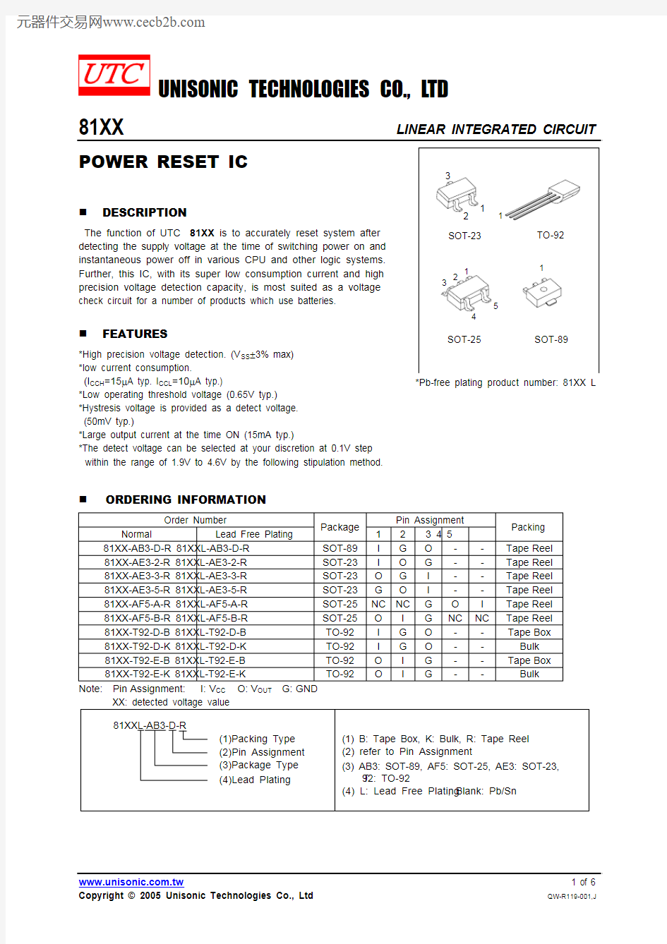
*Pb-free plating product number: 81XX L
ORDERING INFORMATION
Order Number Pin Assignment
Normal Lead Free Plating Package 12 3 4 5
Packing
81XX-AB3-D-R 81XXL-AB3-D-R SOT-89I G O - - Tape Reel 81XX-AE3-2-R 81XXL-AE3-2-R SOT-23I O G - - Tape Reel 81XX-AE3-3-R 81XXL-AE3-3-R SOT-23O G I - - Tape Reel 81XX-AE3-5-R 81XXL-AE3-5-R SOT-23G O I - - Tape Reel 81XX-AF5-A-R 81XXL-AF5-A-R SOT-25NC NC G O I Tape Reel 81XX-AF5-B-R 81XXL-AF5-B-R SOT-25O I G NC NC Tape Reel 81XX-T92-D-B 81XXL-T92-D-B TO-92 I G O - - Tape Box 81XX-T92-D-K 81XXL-T92-D-K TO-92 I G O - - Bulk 81XX-T92-E-B 81XXL-T92-E-B TO-92 O I G - - Tape Box 81XX-T92-E-K 81XXL-T92-E-K TO-92 O I G - - Bulk Note: Pin Assignment: I: V CC O: V OUT G: GND
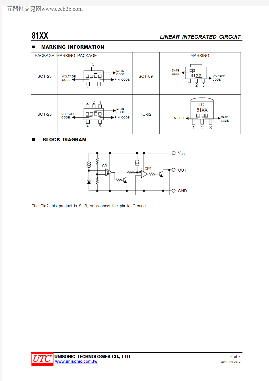
MARKING INFORMATION
BLOCK DIAGRAM
V CC
OUT
GND
The Pin2 this product is SUB, so connect the pin to Ground.
ABSOLUTE MAXIMUM RATINGS
PARAMETER SYMBOL RATINGS UNIT
Power supply voltage V CC -0.3~+10 V Operating temperature T OPR -20~+75 °C Storage temperature T STG -40~+125 °C Note Absolute maximum ratings are those values beyond which the device could be permanently damaged.
Absolute maximum ratings are stress ratings only and functional device operation is not implied.
ELECTRICAL CHARACTERISTICS
(Ta=25°C, The unit of resistance is ? unless otherwise indicated.)
PARAMETER SYMBOL (*1)TEST CONDITIONS MIN TYP MAX UNIT
UTC 8150 4.850 5.000 5.150UTC 8146 4.462 4.600 4.738UTC 8145 4.365 4.500 4.635UTC 8144 4.268 4.400 4.532UTC 8143 4.171 4.300 4.429UTC 8142 4.074 4.200 4.326UTC 8141 3.977 4.100 4.223UTC 8140 3.880 4.000 4.120UTC 8139 3.783 3.900 4.017UTC 8138 3.686 3.800 3.914UTC 8137 3.589 3.700 3.811UTC 8136 3.492 3.600 3.708UTC 8135 3.395 3.500 3.605UTC 8134 3.298 3.400 3.502
UTC 8133 3.201 3.300 3.399
UTC 8132 3.104 3.200 3.296
UTC 8131 3.007 3.100 3.193UTC 8130 2.910 3.000 3.090UTC 8129 2.813 2.900 2.987UTC 8128 2.716 2.800 2.884UTC 8127 2.619 2.700 2.781UTC 8126 2.522 2.600 2.678UTC 8125 2.425 2.500 2.575UTC 8124 2.328 2.400 2.472UTC 8123 2.231 2.300 2.369UTC 8122 2.134 2.200 2.266UTC 8121 2.037 2.100 2.163UTC 8120 1.940 2.000 2.060UTC 8119 1.843 1.900 1.957Detection Voltage V SS 1 R L =470?
V CC =H->L V OUT =V CC
UTC 8118 1.746 1.800 1.854
V
Hysteresis Voltage ?V SS 1
R L =470?, V CC =L->H->L,
V OUT =V CC
30 50 100 mV Detection Voltage Temperature
Coefficient V SS /?T 1 R L =470?, Ta=-20~+75°C V OUT =V CC
±0.01 %/°C
Low Level Output Voltage V OL 1
V CC =V SS min.-0.05V,
R L =470?
0.2 0.4 V Output Leakage Current I OH 2 V CC =10V , V OUT =V CC ±0.1 μA Circuit Current at ON Time I CCL 3 V CC =V SS min.-0.05V, R L =∞ 3 5 μA Circuit Current at OFF Time I CCH 3 V CC =V SS typ./0.85, R L =∞ 3 5 μA
ELECTRICAL CHARACTERISTICS(Cont.)
PARAMETER SYMBOL (*1)TEST CONDITIONS MIN TYP MAX UNIT
“H” Transmission Delay Time TpLH (*2) 4 C L =100pF, R L =4.7K ? 20 60 μS “L” Transmission Delay Time TpHL (*3) 4 C L =100pF, R L =4.7k ? 20 60 μS
Operating Threshold Voltage V OPL 1 R L =4.7k ?, V OL ≦0.4V 0.65 0.85 V Output current at ON Time 1 I OL 1 2
R L =0, V CC =Vs min.-0.05V,
V OUT =0.4V 5 mA Output current at ON Time 2 I OL 2 2 Ta=-20~+75°C
R L =0, V CC =V SS min.-0.15V V OUT =0.4V
3 mA
Note:
(*1) MEASUREMENT CIRCUIT
(*2) TpLH: V CC =(V SS Typ. –0.4V) -> (V SS Typ. +0.4V) (*3) TpHL: V CC =(V SS Typ. +0.4V) -> (V SS Typ. -0.4V)
MEASURING CIRCUITS
V 1
)
V CC
2)
V OUT
V CC
3)
PULSE
5.0V
4)
NOTE: 1.) A: DC AMMETER V: DC VOLTMETER CRT: OSCILLOSCOPE 2.) INPUT PULSE
VsTyp. +0.4V VsTyp. -0.4V
0V