UTCLM324中文资料
UTC LM324
LINEAR INTEGRATED CIRCUIT
UTC UNISONIC TECHNOLOGIES CO., LTD.
1
QW-R105-006,B
QUAD OPERATIONAL AMPLIFIERS
DESCRIPTION
The UTC LM324 consists of four independent, high
gain internally frequency compensated operational amplifiers which are designed specifically to operated from a single power supply over a wide voltage range. Operation from split power supplies is also possible. Application areas include transducer amplifier, DC gain blocks and all the conventional OP amp circuits which now can be easily implemented in single power supply system.
FEATURES
*Internally frequency compensated for unity gain. *Large DC voltage gain :100dB.
*Wide operating supply range (Vcc=3V~32V). *Input common-mode voltage includes ground. *Large output voltage swing: From 0V to Vcc-1.5V. *Power drain suitable for battery operation.
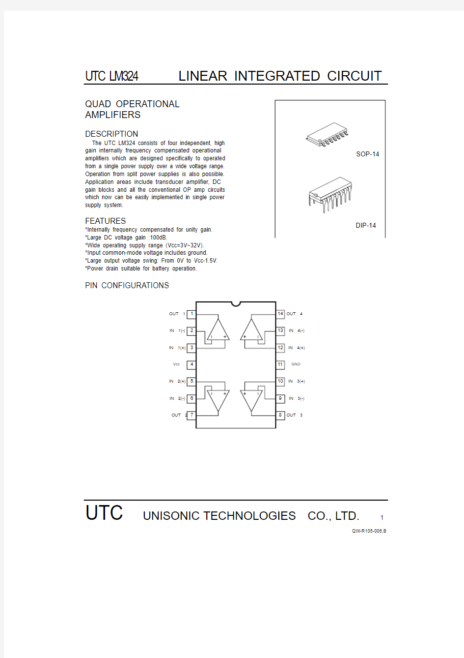
PIN CONFIGURATIONS
1234765OUT 2IN 2(-)IN 1(+)Vcc GND
OUT 1
IN 1(-)IN 2(+)OUT 4
IN 4(-)
IN 4(+)
IN 3(+)
IN 3(-)
OUT 3
891011121314
UTC LM324
LINEAR INTEGRATED CIRCUIT
UTC UNISONIC TECHNOLOGIES CO., LTD.
2
QW-R105-006,B
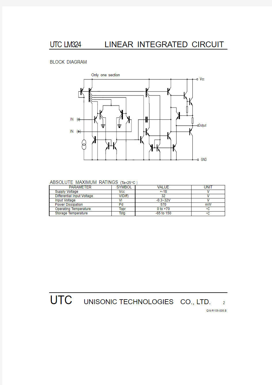
BLOCK DIAGRAM
Only one section
IN (-)
Vcc
GND
ABSOLUTE MAXIMUM RATINGS (Ta=25°C )
PARAMETER SYMBOL
VALUE
UNIT
Supply Voltage
Vcc
+-18 V
Differential Input Voltage VIDiff) 32 V Input Voltage VI -0.3~32V V Power Dissipation Pd 570 mW Operating Temperature Topr 0 to +70 °C Storage Temperature
Tstg
-65 to 150
°C
UTC LM324 LINEAR INTEGRATED CIRCUIT
UTC UNISONIC TECHNOLOGIES CO., LTD.
3
QW-R105-006,B
ELECTRICAL CHARACTERISTICS ( Ta=25°C )
(Vcc=5.0V,All voltage referenced to GND unless otherwise specified)
PARAMETER SYMBOL
TEST CONDITIONS MIN
TYP. MAX UNIT
Input Offset Voltage
V IO
VCM=0 to Vcc=-1.5 Vo(p)=1.4V,Rs=0
7 mV Input Offset Current I IO 50 nA Input Bias Current
Ib 250 nA Input Common-Mode Voltage Range
V I(R) Vcc =30V 0 Vcc-1.5 V
Supply Current Icc RL=∞,Vcc=30V 1.0 3 mA Vcc =
5V 0.7 1.2 mA Large Signal Voltage Gain G V Vcc=15V,RL>2k ?
Vo(p)=1V to 11V
25 100 V/mV V (OH) Vcc=30V,RL=2k ? 26 V Output Voltage Swing Vcc=30V,RL=10k ?
27 28 V V (OL) Vcc=5V,RL>10k ?
5 20 mV Common-Mode Rejection Ratio CMRR 65 75 dB Power Supply Rejection Ratio PSRR 65 100 dB Channel Separation CS f=1kHz to 20kHz 120 dB Short Circuit to GND Isc 40 60 mA Isource VI(+)=1V,VI(-)=0 Vcc=15V,Vo(p)=2V
20 40 mA
Output Current Isink VI(+)=0V,VI(-)=1V Vcc=15V,Vo(p)=2V
10 13 mA
VI(+)=1V,VI(-)=0 Vcc=15V,Vo(p)=200mV
12 45 μA Differential Input Voltage VI(diff) Vcc V
UTC LM324 LINEAR INTEGRATED CIRCUIT
UTC UNISONIC TECHNOLOGIES CO., LTD.
4
QW-R105-006,B
TYPICAL PERFORMANCE CHARACTERISTICS
5
015
Supply Voltage (+- Vdc)
I n p u t v o l t
g a e (V )
㊣0
20
40
60
80
I n p u t c u r r e n t (n A )
Temperature (°C)
12
3
40
S u p p l y C u r r e n t (m A )
Supply Voltage (V)
V o l t g a e G a i n (d B )
Supply Voltage (V)
V o l t a g e G a i n (d B )
20
40
6080
1010
10
1010101010
Frequency (Hz)
10
1010
10
10
2040
6080
C M R R (d B )
Frequency (Hz)
UTC LM324
LINEAR INTEGRATED CIRCUIT
UTC UNISONIC TECHNOLOGIES CO., LTD.
5
QW-R105-006,B
Time (μs)
Fig.9 Large signal Frequency Response
O u t p u t s w i n g (V p -p )
10
-3
10
-2
10
-1
1102
10
10
1
10
O u t p u t V o l t a g e (V )
Output Sink Current (mA)
10
-1
10
-2
10
-3
102
10
1Fig.10 Output Characteristics
current sourcing
O u t p u t r e f f
e r e n c e V c c (V )
Output Source current (mA)
Fig.8 Voltage Follower pulse response
(small signal)
O u t p u t v o l t g a e (V )
1234
56789
275
300350
400
450
I n p u t V o l t a g e (V )
O u t p u t V o l t a g e (V )Time (μs)
10
50Fig.7
-50
-25
025*******
20
40
60
Temperature (°C)
O u t p u t C u r r e n t (m A )
Fig.12 Current
Limiting