AUIRF7343QTR;AUIRF7343Q;中文规格书,Datasheet资料
?09/22/11
AUIRF7343Q
Description
https://www.360docs.net/doc/c815229220.html,
1
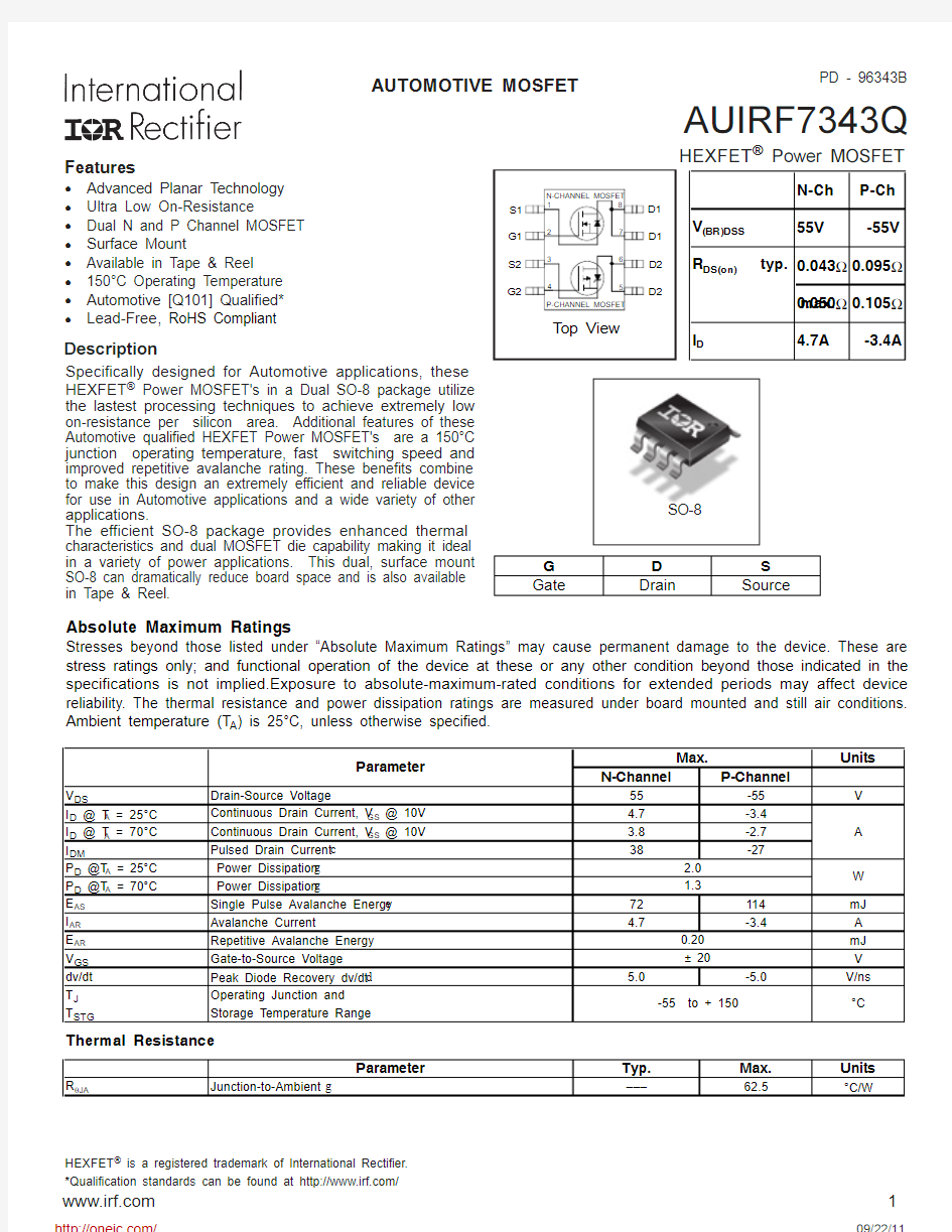
Features
l Advanced Planar Technology
l Ultra Low On-Resistance
l Dual N and P Channel MOSFET l Surface Mount
l Available in Tape & Reel
l 150°C Operating Temperature l Automotive [Q101] Qualified*l
Lead-Free , RoHS Compliant
Specifically designed for Automotive applications, these HEXFET ? Power MOSFET's in a Dual SO-8 package utilize the lastest processing techniques to achieve extremely low on-resistance per silicon area. Additional features of these Automotive qualified HEXFET Power MOSFET's are a 150°C junction operating temperature, fast switching speed and improved repetitive avalanche rating. These benefits combine to make this design an extremely efficient and reliable device for use in Automotive applications and a wide variety of other applications.
The efficient SO-8 package provides enhanced thermal characteristics and dual MOSFET die capability making it ideal in a variety of power applications. This dual, surface mount SO-8 can dramatically reduce board space and is also available in Tape & Reel.
SO-8
PD - 96343B
AUTOMOTIVE MOSFET
Absolute Maximum Ratings
Stresses beyond those listed under “Absolute Maximum Ratings” may cause permanent damage to the device. These are stress ratings only; and functional operation of the device at these or any other condition beyond those indicated in the specifications is not implied.Exposure to absolute-maximum-rated conditions for extended periods may affect device reliability. The thermal resistance and power dissipation ratings are measured under board mounted and still air conditions.Ambient temperature (T A ) is 25°C, unless otherwise specified.
HEXFET ? is a registered trademark of International Rectifier.*Qualification standards can be found at https://www.360docs.net/doc/c815229220.html,/
Thermal Resistance
https://www.360docs.net/doc/c815229220.html,/
AUIRF7343Q
2
https://www.360docs.net/doc/c815229220.html,
Repetitive rating; pulse width limited by max. junction temperature. (See fig. 22 )
Notes:
N-Channel Starting T J = 25°C, L = 6.5mH R G = 25Ω, I AS = 4.7A.
P-Channel Starting T J = 25°C, L = 20mH R G = 25Ω, I AS = -3.4A. Pulse width ≤ 300μs; duty cycle ≤ 2%.
Surface mounted on FR-4 board, t ≤ 10sec.
N-Channel I SD ≤ 4.7A, di/dt ≤ 220A/μs, V DD ≤ V (BR)DSS , T J ≤ 150°C P-Channel I SD ≤ -3.4A, di/dt ≤ -150A/μs, V DD ≤ V (BR)DSS , T J ≤ 150°C
Static Electrical Characteristics @ T
= 25°C (unless otherwise stated)
https://www.360docs.net/doc/c815229220.html,/
AUIRF7343Q
https://www.360docs.net/doc/c815229220.html,
3
Qualification Information
?
? Qualification standards can be found at International Rectifier’s web site: http//https://www.360docs.net/doc/c815229220.html,/?? Exceptions (if any) to AEC-Q101 requirements are noted in the qualification report.??? Highest passing voltage
https://www.360docs.net/doc/c815229220.html,/
AUIRF7343Q
4
https://www.360docs.net/doc/c815229220.html,
Fig 3. Typical Transfer Characteristics
Fig 2. Typical Output Characteristics
Fig 1. Typical Output Characteristics
Forward Voltage
N-Channel
https://www.360docs.net/doc/c815229220.html,/
AUIRF7343Q
https://www.360docs.net/doc/c815229220.html,
5
Fig 5. Normalized On-Resistance
Vs. Temperature
Fig 8. Maximum Avalanche Energy
Vs. Drain Current
Fig 6. Typical On-Resistance Vs. Drain
Current
Fig 7. Typical On-Resistance Vs. Gate Voltage
N-Channel
R D S (o n ) , D r a i n -t o -S o u r c e O n R e s i s t a n c e ( Ω )
0.04
0.06
0.08
0.10
0.120
2
4
6
8
10
GS
V , Gate-to-Source Voltage (V)https://www.360docs.net/doc/c815229220.html,/
AUIRF7343Q
6
https://www.360docs.net/doc/c815229220.html,
Fig 11. Maximum Effective Transient Thermal Impedance, Junction-to-Ambient
Fig 10. Typical Gate Charge Vs.
Gate-to-Source Voltage
Fig 9. Typical Capacitance Vs.
Drain-to-Source Voltage
N-Channel
https://www.360docs.net/doc/c815229220.html,/
AUIRF7343Q
https://www.360docs.net/doc/c815229220.html,
7
Fig 14. Typical Transfer Characteristics
Fig 15. Typical Source-Drain Diode
Forward Voltage
P-Channel
https://www.360docs.net/doc/c815229220.html,/
AUIRF7343Q
8
https://www.360docs.net/doc/c815229220.html,
Fig 16. Normalized On-Resistance
Vs. Temperature
Fig 19. Maximum Avalanche Energy
Vs. Drain Current
Current
Fig 18. Typical On-Resistance Vs. Gate Voltage
P-Channel
R D S (o n ) , D r a i n -t o -S o u r c e O n R e s i s t a n c e ( Ω )
0.05
0.15
0.25
0.35
0.45
2
5
8
11
14
GS
-V , Gate-to-Source Voltage (V)https://www.360docs.net/doc/c815229220.html,/
AUIRF7343Q
https://www.360docs.net/doc/c815229220.html,
9
Fig 21. Typical Gate Charge Vs.
Gate-to-Source Voltage
Fig 20. Typical Capacitance Vs.Drain-to-Source Voltage
P-Channel
Fig 22. Maximum Effective Transient Thermal Impedance, Junction-to-Ambient
https://www.360docs.net/doc/c815229220.html,/
AUIRF7343Q
https://www.360docs.net/doc/c815229220.html,
SO-8 Package Outline
Dimensions are shown in millimeters (inches)
Note: For the most current drawing please refer to IR website at https://www.360docs.net/doc/c815229220.html,/package/
https://www.360docs.net/doc/c815229220.html,/
分销商库存信息:
IR
AUIRF7343QTR AUIRF7343Q