vp230
https://www.360docs.net/doc/c418342871.html, FEATURES
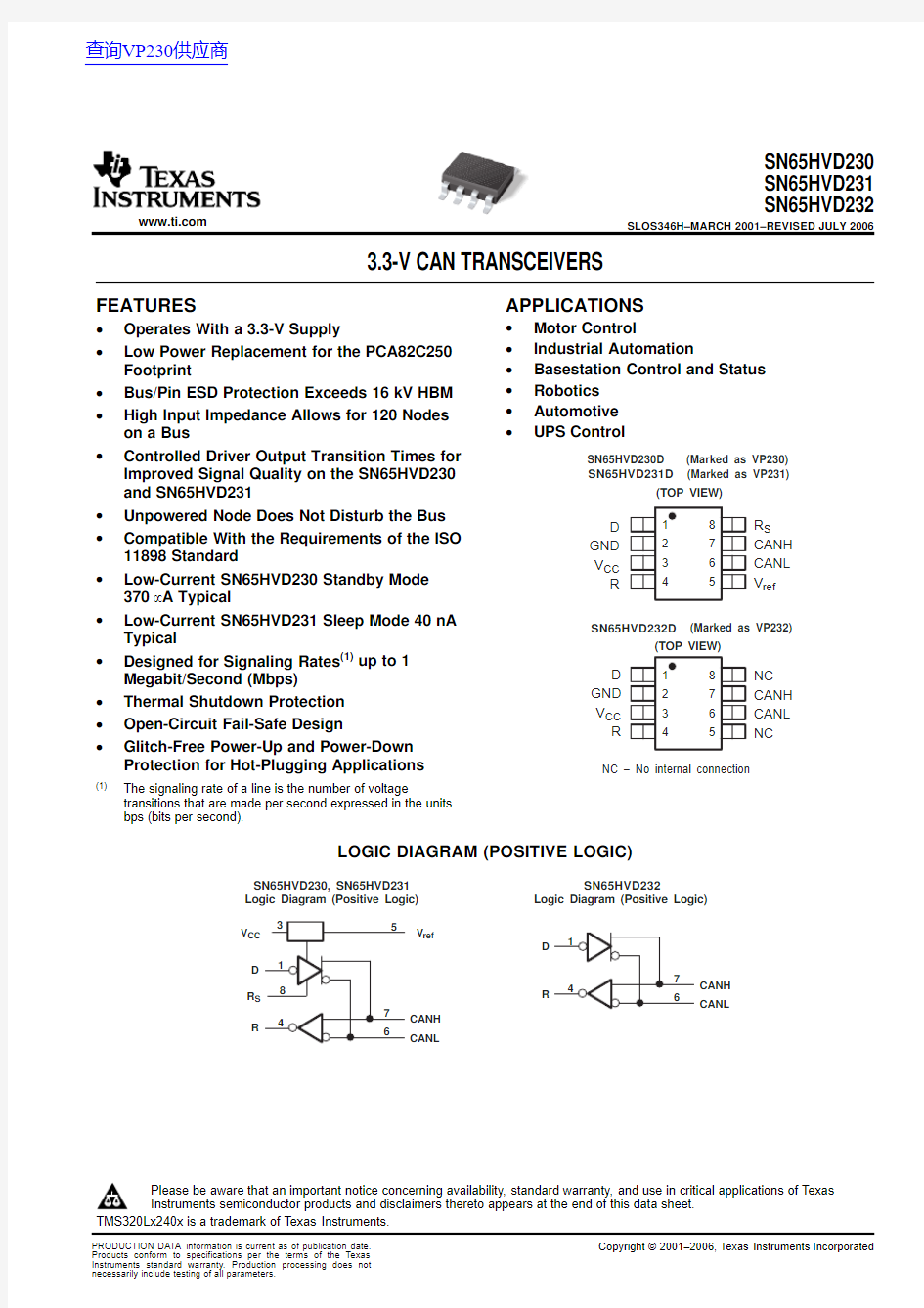
APPLICATIONS D GND V CC R R S CANH CANL V ref SN65HVD230D (Marked as VP230)SN65HVD231D (Marked as VP231)(TOP VIEW)
NC – No internal connection
D GND V CC R NC CANH CANL NC SN65HVD232D (Marked as VP232)(TOP VIEW)
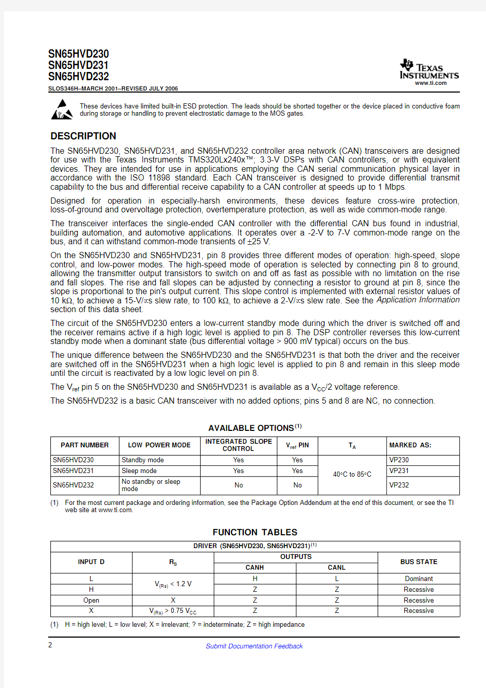
LOGIC DIAGRAM (POSITIVE LOGIC)
CANL CANH R
D
SN65HVD230, SN65HVD231
Logic Diagram (Positive Logic)
R S
V ref V CC
CANL CANH R
D SN65HVD232Logic Diagram (Positive Logic)SN65HVD230SN65HVD231SN65HVD232SLOS346H–MARCH 2001–REVISED JULY 2006
3.3-V CAN TRANSCEIVERS
?Motor Control ?
Operates With a 3.3-V Supply ?Industrial Automation ?
Low Power Replacement for the PCA82C250?Basestation Control and Status Footprint ?Robotics ?
Bus/Pin ESD Protection Exceeds 16kV HBM ?Automotive ?
High Input Impedance Allows for 120Nodes ?UPS Control on a Bus ?Controlled Driver Output Transition Times for
Improved Signal Quality on the SN65HVD230
and SN65HVD231
?Unpowered Node Does Not Disturb the Bus
?Compatible With the Requirements of the ISO
11898Standard
?Low-Current SN65HVD230Standby Mode
370μA Typical
?Low-Current SN65HVD231Sleep Mode 40nA
Typical
?Designed for Signaling Rates (1)up to 1
Megabit/Second (Mbps)
?Thermal Shutdown Protection
?Open-Circuit Fail-Safe Design
?Glitch-Free Power-Up and Power-Down
Protection for Hot-Plugging Applications
(1)The signaling rate of a line is the number of voltage
transitions that are made per second expressed in the units
bps (bits per second).Please be aware that an important notice concerning availability,standard warranty,and use in critical applications of Texas
Instruments semiconductor products and disclaimers thereto appears at the end of this data sheet.
查询VP230供应商
https://www.360docs.net/doc/c418342871.html, DESCRIPTION
FUNCTION TABLES
SN65HVD230
SN65HVD231
SN65HVD232
SLOS346H–MARCH2001–REVISED JULY2006
These devices have limited built-in ESD protection.The leads should be shorted together or the device placed in conductive foam during storage or handling to prevent electrostatic damage to the MOS gates.
The SN65HVD230,SN65HVD231,and SN65HVD232controller area network(CAN)transceivers are designed for use with the Texas Instruments TMS320Lx240x?;3.3-V DSPs with CAN controllers,or with equivalent devices.They are intended for use in applications employing the CAN serial communication physical layer in accordance with the ISO11898standard.Each CAN transceiver is designed to provide differential transmit capability to the bus and differential receive capability to a CAN controller at speeds up to1Mbps.
Designed for operation in especially-harsh environments,these devices feature cross-wire protection, loss-of-ground and overvoltage protection,overtemperature protection,as well as wide common-mode range. The transceiver interfaces the single-ended CAN controller with the differential CAN bus found in industrial, building automation,and automotive applications.It operates over a-2-V to7-V common-mode range on the bus,and it can withstand common-mode transients of±25V.
On the SN65HVD230and SN65HVD231,pin8provides three different modes of operation:high-speed,slope control,and low-power modes.The high-speed mode of operation is selected by connecting pin8to ground, allowing the transmitter output transistors to switch on and off as fast as possible with no limitation on the rise and fall slopes.The rise and fall slopes can be adjusted by connecting a resistor to ground at pin8,since the slope is proportional to the pin's output current.This slope control is implemented with external resistor values of 10k?,to achieve a15-V/μs slew rate,to100k?,to achieve a2-V/μs slew rate.See the Application Information section of this data sheet.
The circuit of the SN65HVD230enters a low-current standby mode during which the driver is switched off and the receiver remains active if a high logic level is applied to pin8.The DSP controller reverses this low-current standby mode when a dominant state(bus differential voltage>900mV typical)occurs on the bus.
The unique difference between the SN65HVD230and the SN65HVD231is that both the driver and the receiver are switched off in the SN65HVD231when a high logic level is applied to pin8and remain in this sleep mode until the circuit is reactivated by a low logic level on pin8.
The V ref pin5on the SN65HVD230and SN65HVD231is available as a V CC/2voltage reference.
The SN65HVD232is a basic CAN transceiver with no added options;pins5and8are NC,no connection.
AVAILABLE OPTIONS(1)
INTEGRATED SLOPE
PART NUMBER LOW POWER MODE V ref PIN T A MARKED AS:
CONTROL
SN65HVD230Standby mode Yes Yes VP230
SN65HVD231Sleep mode Yes Yes VP231
40°C to85°C
No standby or sleep
SN65HVD232No No VP232
mode
(1)For the most current package and ordering information,see the Package Option Addendum at the end of this document,or see the TI
web site at https://www.360docs.net/doc/c418342871.html,.
DRIVER(SN65HVD230,SN65HVD231)(1)
OUTPUTS
INPUT D R S BUS STATE
CANH CANL
L H L Dominant
V(Rs)<1.2V
H Z Z Recessive
Open X Z Z Recessive
X V(Rs)>0.75V CC Z Z Recessive
(1)H=high level;L=low level;X=irrelevant;?=indeterminate;Z=high impedance
https://www.360docs.net/doc/c418342871.html,
TERMINAL FUNCTIONS
SN65HVD230
SN65HVD231
SN65HVD232 SLOS346H–MARCH2001–REVISED JULY2006
DRIVER(SN65HVD232)(1)
OUTPUTS
INPUT D BUS STATE
CANH CANL
L H L Dominant
H Z Z Recessive
Open Z Z Recessive (1)H=high level;L=low level;Z=high impedance
RECEIVER(SN65HVD230)(1)
DIFFERENTIAL INPUTS R S OUTPUT R V ID≥0.9V X L
0.5V V ID≤0.5V X H Open X H (1)H=high level;L=low level;X=irrelevant;?=indeterminate RECEIVER(SN65HVD231)(1) DIFFERENTIAL INPUTS R S OUTPUT R V ID≥0.9V L 0.5V V ID≤0.5V H X V(Rs)>0.75V CC H X 1.2V Open X H (1)H=high level;L=low level;X=irrelevant;?=indeterminate RECEIVER(SN65HVD232)(1) DIFFERENTIAL INPUTS OUTPUT R V ID≥0.9V L 0.5V V ID≤0.5V H Open H (1)H=high level;L=low level;X=irrelevant;?=indeterminate TRANSCEIVER MODES(SN65HVD230,SN65HVD231) V(Rs)OPERATING MODE V(Rs)>0.75V CC Standby 10k?to100k?to ground Slope control V(Rs)<1V High speed(no slope control) TERMINAL DESCRIPTION NAME NO. SN65HVD230,SN65HVD231 CANL6Low bus output CANH7High bus output D1Driver input GND2Ground R4Receiver output https://www.360docs.net/doc/c418342871.html, EQUIVALENT INPUT AND OUTPUT SCHEMATIC DIAGRAMS V CC D Input Input Output CANH and CANL Outputs V CC Output R Output Input CANH and CANL Inputs SN65HVD230SN65HVD231SN65HVD232 SLOS346H–MARCH 2001–REVISED JULY 2006TERMINAL FUNCTIONS (continued) TERMINAL DESCRIPTION NAME NO.R S 8Standby/slope control V CC 3Supply voltage V ref 5Reference output SN65HVD232 CANL 6Low bus output CANH 7High bus output D 1Driver input GND 2Ground NC 5,8No connection R 4Receiver output V CC 3Supply voltage https://www.360docs.net/doc/c418342871.html, ABSOLUTE MAXIMUM RATINGS RECOMMENDED OPERATING CONDITIONS SN65HVD230 SN65HVD231 SN65HVD232 SLOS346H–MARCH2001–REVISED JULY2006 over operating free-air temperature range(unless otherwise noted)(1)(2) UNIT Supply voltage range,V CC-0.3V to6V Voltage range at any bus terminal(CANH or CANL)-4V to16V Voltage input range,transient pulse,CANH and CANL,through100?(see Figure7)-25V to25V Input voltage range,V I(D or R)-0.5V to V CC+0.5V Receiver output current,I O±11mA CANH,CANL and GND16kV Human body model(3) Electrostatic discharge All Pins4kV Charged-device model(4)All pins1kV Continuous total power dissipation See Dissipation Rating Table (1)Stresses beyond those listed under"absolute maximum ratings"may cause permanent damage to the device.These are stress ratings only,and functional operation of the device at these or any other conditions beyond those indicated under"recommended operating conditions"is not implied.Exposure to absolute-maximum-rated conditions for extended periods amy affect device reliability. (2)All voltage values,except differential I/O bus voltages,are with respect to network ground terminal. (3)Tested in accordance with JEDEC Standard22,Test Method A114-A. (4)Tested in accordance with JEDEC Standard22,Test Method C101. DISSIPATION RATING TABLE T A≤25°C DERATING FACTOR(1)T A=70°C T A=85°C PACKAGE POWER RATING ABOVE T A=25°C POWER RATING POWER RATING D725mW 5.8mW/°C464mW377mW (1)This is the inverse of the junction-to-ambient thermal resistance when board-mounted and with no air flow. MIN NOM MAX UNIT Supply voltage,V CC3 3.6V Voltage at any bus terminal(common mode)V IC-2(1)7V Voltage at any bus terminal(separately)V I-2.57.5V High-level input voltage,V IH D,R2V Low-level input voltage,V IL D,R0.8V Differential input voltage,V ID(see Figure5)-66V Input voltage,V(Rs)0V CC V Input voltage for standby or sleep,V(Rs)0.75V CC V CC V Wave-shaping resistance,Rs0100k? Driver-40 High-level output current,I OH mA Receiver-8 Driver48 Low-level output current,I OL mA Receiver8 Operating free-air temperature,T A-4085°C (1)The algebraic convention,in which the least positive(most negative)limit is designated as minimum is used in this data sheet. https://www.360docs.net/doc/c418342871.html, DRIVER ELECTRICAL CHARACTERISTICS DRIVER SWITCHING CHARACTERISTICS SN65HVD230SN65HVD231SN65HVD232 SLOS346H–MARCH 2001–REVISED JULY 2006over recommended operating conditions (unless otherwise noted) PARAMETER TEST CONDITIONS MIN TYP (1)MAX UNIT CANH 2.45V CC V I =0V,V OH Dominant See Figure 1and Figure 3CANL 0.5 1.25Bus output V voltage CANH 2.3V I =3V,V OL Recessive See Figure 1and Figure 3CANL 2.3V I =0V,See Figure 1 1.523V OD(D) Dominant V V I =0V,See Figure 2 1.223Differential output voltage V I =3V,See Figure 1-120012mV V OD(R) Recessive V I =3V,No load -0.5-0.20.05V I IH High-level input current V I =2V -30μA I IL Low-level input current V I =0.8V -30μA V CANH =-2V -250250I OS Short-circuit output current mA V CANL =7V -250250C o Output capacitance See receiver Standby SN65HVD230V (Rs)=V CC 370600μA Sleep SN65HVD231V (Rs)=V CC ,D at V CC 0.041Supply I CC current Dominant V I =0V,No load Dominant 1017All devices mA Recessive V I =V CC ,No load Recessive 1017(1)All typical values are at 25°C and with a 3.3-V supply. over recommended operating conditions (unless otherwise noted) TEST PARAMETER MIN TYP MAX UNIT CONDITIONS SN65HVD230AND SN65HVD231 V (Rs)=0V 3585Propagation delay time,low-to-high-level t PLH R S with 10k ?to ground 70125ns output R S with 100k ?to ground 500870V (Rs)=0V 70120Propagation delay time,high-to-low-level t PHL R S with 10k ?to ground 130180ns output R S with 100k ?to ground 8701200V (Rs)=0V 35C L =50pF,t sk(p) Pulse skew (|t PHL -t PLH |)R S with 10k ?to ground 60ns See Figure 4R S with 100k ?to ground 370t r Differential output signal rise time 2550100ns V (Rs)=0V t f Differential output signal fall time 405580ns t r Differential output signal rise time 80120160ns R S with 10k ?to ground t f Differential output signal fall time 80125150ns t r Differential output signal rise time 6008001200ns R S with 100k ?to ground t f Differential output signal fall time 6008251000ns SN65HVD232t PLH Propagation delay time,low-to-high-level output 3585t PHL Propagation delay time,high-to-low-level output 70120C L =50pF,t sk(p) Pulse skew (|t PHL -t PLH |)35ns See Figure 4t r Differential output signal rise time 2550100t f Differential output signal fall time 405580 https://www.360docs.net/doc/c418342871.html, RECEIVER ELECTRICAL CHARACTERISTICS RECEIVER SWITCHING CHARACTERISTICS DEVICE SWITCHING CHARACTERISTICS DEVICE CONTROL-PIN CHARACTERISTICS SN65HVD230 SN65HVD231 SN65HVD232 SLOS346H–MARCH2001–REVISED JULY2006 over recommended operating conditions(unless otherwise noted) PARAMETER TEST CONDITIONS MIN TYP(1)MAX UNIT V IT+Positive-going input threshold voltage750900mV See Table1 V IT-Negative-going input threshold voltage500650 mV V hys Hysteresis voltage(V IT+-V IT-)100 V OH High-level output voltage-6V≤V ID≤500mV,I O=-8mA,See Figure5 2.4 V V OL Low-level output voltage900mV≤V ID≤6V,I O=8mA,See Figure50.4 V IH=7V100250 μA V IH=7V,V CC=0V100350 Other input at0V, I I Bus input current D=3V V IH=-2V-200-30 μA V IH=-2V,V CC=0V-100-20 Pin-to-ground, C i CANH,CANL input capacitance V(D)=3V,32pF V I=0.4sin(4E6πt)+0.5V Pin-to-pin, C diff Differential input capacitance V(D)=3V,16pF V I=0.4sin(4E6πt)+0.5V R diff Differential input resistance Pin-to-pin,V(D)=3V4070100k?R I CANH,CANL input resistance203550k? I CC Supply current See driver (1)All typical values are at25°C and with a3.3-V supply. over recommended operating conditions(unless otherwise noted) PARAMETER TEST CONDITIONS MIN TYP MAX UNIT t PLH Propagation delay time,low-to-high-level output3550ns t PHL Propagation delay time,high-to-low-level output See Figure63550ns t sk(p)Pulse skew(|t PHL-t PLH|)10ns t r Output signal rise time 1.5ns See Figure6 t f Output signal fall time 1.5ns over recommended operating conditions(unless otherwise noted) PARAMETER TEST CONDITIONS MIN TYP MAX UNIT V(Rs)=0V,See Figure970115 Total loop delay,driver input to receiver t(LOOP1)R S with10k?to ground,See Figure9105175ns output,recessive to dominant R S with100k?to ground,See Figure9535920 V(Rs)=0V,See Figure9100135 Total loop delay,driver input to receiver t(LOOP2)R S with10k?to ground,See Figure9155185ns output,dominant to recessive R S with100k?to ground,See Figure9830990 over recommended operating conditions(unless otherwise noted) PARAMETER TEST CONDITIONS MIN TYP(1)MAX UNIT SN65HVD230wake-up time from standby mode 0.55 1.5μs with R S t(WAKE)See Figure8 SN65HVD231wake-up time from sleep mode with 35μs R S https://www.360docs.net/doc/c418342871.html, PARAMETER MEASUREMENT INFORMATION 0 V or 3 V –2 V ≤ V TEST ≤ 7 V ≈ 2.3 V Dominant V OL ≈ 3 V V OH ≈ 1 V V OH SN65HVD230SN65HVD231SN65HVD232 SLOS346H–MARCH 2001–REVISED JULY 2006DEVICE CONTROL-PIN CHARACTERISTICS (continued) over recommended operating conditions (unless otherwise noted) PARAMETER TEST CONDITIONS MIN TYP (1)MAX UNIT -5μA Reference output voltage V -50μA Figure 1.Driver Voltage and Current Definitions Figure 2.Driver V OD Figure 3.Driver Output Voltage Definitions https://www.360docs.net/doc/c418342871.html, Output V OD(R) V OD(D)V IC +V CANH )V CANL 2SN65HVD230SN65HVD231SN65HVD232SLOS346H–MARCH 2001–REVISED JULY 2006 PARAMETER MEASUREMENT INFORMATION (continued) A. The input pulse is supplied by a generator having the following characteristics:PRR ≤500kHz,50%duty cycle,t r ≤6ns,t f ≤6ns,Z o =50?.B.C L includes probe and jig capacitance. Figure 4.Driver Test Circuit and Voltage Waveforms Figure 5.Receiver Voltage and Current Definitions https://www.360docs.net/doc/c418342871.html, C L = 15 pF (see Note B) V OL V OH SN65HVD230SN65HVD231SN65HVD232 SLOS346H–MARCH 2001–REVISED JULY 2006PARAMETER MEASUREMENT INFORMATION (continued) A. The input pulse is supplied by a generator having the following characteristics:PRR ≤500kHz,50%duty cycle,t r ≤6ns,t f ≤6ns,Z o =50?.B.C L includes probe and jig capacitance. Figure 6.Receiver Test Circuit and Voltage Waveforms Figure 7.Overvoltage Protection https://www.360docs.net/doc/c418342871.html, 10 k ? R Output V (Rs) 1.5 V Generator PRR = 150 kHz 50% Duty Cycle t r , t f < 6 ns Z o = 50 ?0 V V CC SN65HVD230SN65HVD231SN65HVD232SLOS346H–MARCH 2001–REVISED JULY 2006 PARAMETER MEASUREMENT INFORMATION (continued) Table 1.Receiver Characteristics Over Common Mode With V (Rs)=1.2V V IC V ID V CANH V CANL R OUTPUT -2V 900mV -1.55V -2.45V L 7V 900mV 8.45V 6.55V L V OL 1V 6V 4V -2V L 4V 6V 7V 1V L -2V 500mV -1.75V -2.25V H 7V 500mV 7.25V 6.75V H 1V -6V -2V 4V H V OH 4V -6V 1V 7V H X X Open Open H Figure 8.t (WAKE)Test Circuit and Voltage Waveforms https://www.360docs.net/doc/c418342871.html, 60 ? ±1% V CC 0 V V OH V OL TYPICAL CHARACTERISTICS ?16?14?12?10?8?6?4?2000.6 1.1 1.6 2.1 2.6 3.1 3.6 I I (L )? L o g i c I n p u t C u r r e n t ? A μV I ? Input Voltage ? V 181614 13 0250500 1921 f ? Frequency ? kbps 22 7501000201715 I C C ? S u p p l y C u r r e n t (R M S ) ? m A SN65HVD230SN65HVD231SN65HVD232 SLOS346H–MARCH 2001–REVISED JULY 2006A.All V I input pulses are supplied by a generator having the following characteristics:t r or t f ≤6ns,Pulse Repetition Rate (PRR)=125kHz,50%duty cycle. Figure 9.t (LOOP)Test Circuit and Voltage Waveforms SUPPLY CURRENT (RMS)LOGIC INPUT CURRENT (PIN D)vs vs FREQUENCY INPUT VOLTAGE Figure 10.Figure 11. https://www.360docs.net/doc/c418342871.html, 0 1234 I O L ? D r i v e r L o w -L e v e l O u t p u t C u r r e n t ? m A V O(CANL) ? Low-Level Output Voltage ? V 020406080100120140160?7?6?4?3?10134678101112I I ? B u s I n p u t C u r r e n t ?A μV I ? Bus Input Voltage ? V ?55?400257085125V O D ? D o m i n a n t V o l t a g e ? V T A ? Free-Air Temperature ? °C 020406080100120 00.51 1.52 2.53 3.5 ? D r i v e r H i g h -L e v e l O u t p u t C u r r e n t ? m A V O(CANH) ? High-Level Output Voltage ? V I O H SN65HVD230SN65HVD231SN65HVD232SLOS346H–MARCH 2001–REVISED JULY 2006 TYPICAL CHARACTERISTICS (continued) BUS INPUT CURRENT DRIVER LOW-LEVEL OUTPUT CURRENT vs vs BUS INPUT VOLTAGE LOW-LEVEL OUTPUT VOLTAGE Figure 12. Figure 13.DRIVER HIGH-LEVEL OUTPUT CURRENT DOMINANT VOLTAGE (V OD )vs vs HIGH-LEVEL OUTPUT VOLTAGE FREE-AIR TEMPERATURE Figure 14.Figure 15. https://www.360docs.net/doc/c418342871.html, ?55?400257085125 t P L H ? R e c e i v e r L o w -t o -H i g h P r o p a g a t i o n D e l a y T i m e ? n s T A ? Free-Air Temperature ? ° C t P H L ? R e c e i v e r H i g h -t o -L o w P r o p a g a t i o n D e l a y T i m e ? n s T A ? Free-Air Temperature ? °C t P L H ? D r i v e r L o w -t o -H i g h P r o p a g a t i o n D e l a y T i m e ? n s T A ? Free-Air Temperature ? °C t P H L ? D r i v e r H i g h -t o -L o w P r o p a g a t i o n D e l a y T i m e ? n s T A ? Free-Air Temperature ? °C SN65HVD230SN65HVD231SN65HVD232 SLOS346H–MARCH 2001–REVISED JULY 2006TYPICAL CHARACTERISTICS (continued) RECEIVER LOW-TO-HIGH PROPAGATION DELAY TIME RECEIVER HIGH-TO-LOW PROPAGATION DELAY TIME vs vs FREE-AIR TEMPERATURE FREE-AIR TEMPERATURE Figure 16. Figure 17.DRIVER LOW-TO-HIGH PROPAGATION DELAY TIME DRIVER HIGH-TO-LOW PROPAGATION DELAY TIME vs vs FREE-AIR TEMPERATURE FREE-AIR TEMPERATURE Figure 18.Figure 19. https://www.360docs.net/doc/c418342871.html, t P L H ? D r i v e r L o w -t o -H i g h P r o p a g a t i o n D e l a y T i m e ? n s T A ? Free-Air Temperature ? ° C t P H L ? D r i v e r H i g h -t o -L o w P r o p a g a t i o n D e l a y T i m e ? n s T A ? Free-Air Temperature ? ° C t P L H ? D r i v e r L o w -t o -H i g h P r o p a g a t i o n D e l a y T i m e ? n s T A ? Free-Air Temperature ? ° C t P H L ? D r i v e r H i g h -t o -L o w P r o p a g a t i o n D e l a y T i m e ? n s T A ? Free-Air Temperature ? °C SN65HVD230SN65HVD231SN65HVD232SLOS346H–MARCH 2001–REVISED JULY 2006 TYPICAL CHARACTERISTICS (continued) DRIVER LOW-TO-HIGH PROPAGATION DELAY TIME DRIVER HIGH-TO-LOW PROPAGATION DELAY TIME vs vs FREE-AIR TEMPERATURE FREE-AIR TEMPERATURE Figure 20. Figure 21.DRIVER LOW-TO-HIGH PROPAGATION DELAY TIME DRIVER HIGH-TO-LOW PROPAGATION DELAY TIME vs vs FREE-AIR TEMPERATURE FREE-AIR TEMPERATURE Figure 22.Figure 23. https://www.360docs.net/doc/c418342871.html, 010********* 1.52 2.53 3.54I O ? D r i v e r O u t p u t C u r r e n t ? m A V CC ? Supply Voltage ? V 0.10 0.20 0.30 0.40 0.50 0.60 0.70 0.80 0.90 1.00 1.10 1.20 1.30 1.40 050100150200 1.50 t f ? D i f f e r e n t i a l D r i v e r O u t p u t F a l l T i m e ? s μ R s ? Source Resistance ? k ??2147 t P L H ? L o w -t o -H i g h P r o p a g a t i o n D e l a y T i m e ? n s V IC ? Common-Mode Input Voltage ? V V r e f ? R e f e r e n c e V o l t a g e ? V I ref ? Reference Current ? μA SN65HVD230SN65HVD231SN65HVD232 SLOS346H–MARCH 2001–REVISED JULY 2006TYPICAL CHARACTERISTICS (continued) DRIVER OUTPUT CURRENT DIFFERENTIAL DRIVER OUTPUT FALL TIME vs vs SUPPLY VOLTAGE SOURCE RESISTANCE (R s )Figure 24.Figure 25. HVD230,HVD231LOW-TO-HIGH PROPAGATION DELAY REFERENCE VOLTAGE TIME vs vs REFERENCE CURRENT COMMON-MODE INPUT VOLTAGE Figure 26.Figure 27. https://www.360docs.net/doc/c418342871.html, V IC ? Common-Mode Input Voltage ? V t P L H ? L o w -t o -H i g h P r o p a g a t i o n D e l a y T i m e ? n s ?2147t P L H ? L o w -t o -H i g h P r o p a g a t i o n D e l a y T i m e ? n s V IC ? Common-Mode Input Voltage ? V ?2 V ≤ V IC ≤ 7 V SN65HVD230SN65HVD231SN65HVD232SLOS346H–MARCH 2001–REVISED JULY 2006 TYPICAL CHARACTERISTICS (continued) HVD230,HVD231LOW-TO-HIGH PROPAGATION DELAY TIME HVD232LOW-TO-HIGH PROPAGATION DELAY TIME vs vs COMMON-MODE INPUT VOLTAGE COMMON-MODE INPUT VOLTAGE Figure 28. Figure 29.Figure 30.Driver Schematic https://www.360docs.net/doc/c418342871.html, APPLICATION INFORMATION INTRODUCTION APPLICATION OF THE SN65HVD230 SN65HVD230SN65HVD231SN65HVD232 SLOS346H–MARCH 2001–REVISED JULY 2006This application provides information concerning the implementation of the physical medium attachment layer in a CAN network according to the ISO 11898standard.It presents a typical application circuit and test results,as well as discussions on slope control,total loop delay,and interoperability in 5-V systems. ISO 11898is the international standard for high-speed serial communication using the controller area network (CAN)bus protocol.It supports multimaster operation,real-time control,programmable data rates up to 1Mbps,and powerful redundant error checking procedures that provide reliable data transmission.It is suited for networking intelligent devices as well as sensors and actuators within the rugged electrical environment of a machine chassis or factory floor.The SN65HVD230family of 3.3-V CAN transceivers implement the lowest layers of the ISO/OSI reference model.This is the interface with the physical signaling output of the CAN controller of the Texas Instruments TMS320Lx240x 3.3-V DSPs,as illustrated in Figure 31. Figure 31.The Layered ISO 11898Standard Architecture The SN65HVD230family of CAN transceivers are compatible with the ISO 11898standard;this ensures interoperability with other standard-compliant products. Figure 32illustrates a typical application of the SN65HVD230family.The output of a DSP's CAN controller is connected to the serial driver input,pin D,and receiver serial output,pin R,of the transceiver.The transceiver is then attached to the differential bus lines at pins CANH and CANL.Typically,the bus is a twisted pair of wires with a characteristic impedance of 120?,in the standard half-duplex multipoint topology of Figure 33.Each end of the bus is terminated with 120-?resistors in compliance with the standard to minimize signal reflections on the bus. https://www.360docs.net/doc/c418342871.html, 120 ?120 ? FEATURES of the SN65HVD230,SN65HVD231,and SN65HVD232SN65HVD230 SN65HVD231 SN65HVD232 SLOS346H–MARCH2001–REVISED JULY2006 APPLICATION INFORMATION(continued) Figure32.Details of a Typical CAN Node Figure33.Typical CAN Network The SN65HVD230/231/2323.3-V CAN transceivers provide the interface between the3.3-V TMS320Lx2403/6/7 CAN DSPs and the differential bus line,and are designed to transmit data at signaling rates up to1Mbps as defined by the ISO11898standard. The SN65HVD230/231/232are pin-compatible(but not functionally identical)with one another and,depending upon the application,may be used with identical circuit boards. These transceivers feature3.3-V operation and standard compatibility with signaling rates up to1Mbps,and also offer16-kV HBM ESD protection on the bus pins,thermal shutdown protection,bus fault protection,and open-circuit receiver failsafe.The fail-safe design of the receiver assures a logic high at the receiver output if the bus wires become open circuited.If a high ambient operating environment temperature or excessive output current result in thermal shutdown,the bus pins become high impedance,while the D and R pins default to a logic high. https://www.360docs.net/doc/c418342871.html, OPERATING MODES High-Speed D GND V CC R 1 1 Mbps Driver Output NRZ Data SN65HVD230 SN65HVD231 SN65HVD232 SLOS346H–MARCH2001–REVISED JULY2006 APPLICATION INFORMATION(continued) The bus pins are also maintained in a high-impedance state during low V CC conditions to ensure glitch-free power-up and power-down bus protection for hot-plugging applications.This high-impedance condition also means that an unpowered node does not disturb the bus.Transceivers without this feature usually have a very low output impedance.This results in a high current demand when the transceiver is unpowered,a condition that could affect the entire bus. R S(pin8)of the SN65HVD230and SN65HVD231provides for three different modes of operation:high-speed mode,slope-control mode,and low-power mode. The high-speed mode can be selected by applying a logic low to R S(pin8).The high-speed mode of operation is commonly employed in industrial applications.High-speed allows the output to switch as fast as possible with no internal limitation on the output rise and fall slopes.The only limitations of the high-speed operation are cable length and radiated emission concerns,each of which is addressed by the slope control mode of operation. If the low-power standby mode is to be employed in the circuit,direct connection to a DSP output pin can be used to switch between a logic-low level(<1V)for high speed operation,and the logic-high level(>0.75V CC) for standby.Figure34shows a typical DSP connection,and Figure35shows the HVD230driver output signal in high-speed mode on the CAN bus. Figure34.R S(Pin8)Connection to a TMS320LF2406/07for High Speed/Standby Operation Figure35.Typical High Speed SN65HVD230Output Waveform Into a60-?Load 74A VC8T245DGVRE4 TI TVSOP24 具有可配置电压转换和 3 态输出的 8 位双电源总线收发器 74A VC8T245PWR TI TSSOP24 具有可配置电压转换和 3 态输出的 8 位双电源总线收发器 74A VCA164245VRE4 TI TVSOP48 具有可配置电压转换和 3 态输出的 16 位双电源总线收发器 74A VCAH164245GRG4 TI TSSOP48 74A VCB164245GR TI TSSOP48 16 位双电源总线收发器,具有可配置转换和三态输出 74A VCB164245VRE4 TI TVSOP48 16 位双电源总线收发器,具有可配置转换和三态输出 74A VCBH164245VRE4 TI TVSOP48 16 位双电源总线收发器,具有可配置电压转换和三态输出 74A VCH16T245VRE4 TI TVSOP48 具有可配置电压转换和 3 态输出的 16 位双电源总线收发器 74A VCH20T245VRE4 TI TVSOP56 具有可配置电压转换和三态输出的 20 位双电源总线收发器 74A VCH4T245PWR TI TSSOP16 74BCT125ADR TI SOP14 具有三态输出的四路总线缓冲器闸 74BCT244DWR TI SOP20 具有三态输出的八路缓冲器/驱动器 74BCT245DWR TI SOP20 八路总线收发器 74BCT573DWR TI SOP20 八路 D 类透明锁存器 74CB3Q16210DGVRE4 TI TVSOP48 20 位 FET 总线开关,2.5V/3.3V 低压高带宽总线开关 74CB3Q16211DGGRE4 TI TSSOP56 24 位 FET、2.5V/3.3V、低压高带宽总线开关 74CB3Q16244DGGRE4 TI TSSOP48 16 位 FET 总线开关,2.5V/3.3V 低压高带宽总线开关 74CB3Q16244DGVRE4 TI TVSOP48 16 位 FET 总线开关,2.5V/3.3V 低压高带宽总线开关 74CB3Q16245DGVRE4 TI TVSOP48 16 位 FET 总线开关,2.5V/3.3V、低压高带宽总线开关 74CB3Q3125PWR TI TSSOP14 四路 FET、2.5V/3.3V、低压高带宽总线开关 74CB3Q3244PWR TI TSSOP20 74CB3Q3245DBQRG4 TI QSOP20 8 位 2.5V/3.3V 低电压 FET 总线开关 74CB3Q3245PWR TI TSSOP20 74CB3Q3253PWR TI TSSOP16 双路 4 选 1 FET 多路复用器/多路解复用器,2.5V/3.3V 低电压高带宽总线开关 74CB3Q3257DGVRE4 TI TVSOP16 4 位 2 选 1 FET 多路复用器/多路解复用器,2.5V/3.3V 低压高带宽总线开关 74CB3Q3257PWR TI TSSOP16 74CB3Q3305PWR TI TSSOP8 74CB3Q3306APWRE4 TI TSSOP8 双路 FET 2.5V/3.3V 低电压高带宽总线开关 74CB3Q3345DGVRE4 TI TVSOP24 8 位 FET、2.5V/3.3V、低压高带宽总线开关 74CB3Q3384ADBQR TI QSOP24 10 位 2.5V/3.3V 低电压 FET 总线开关 74CB3Q3384ADGVRE4 TI TVSOP24 10 位 2.5V/3.3V 低电压 FET 总线开关 74CB3Q3384APWR TI TSSOP24 10 位 2.5V/3.3V 低电压 FET 总线开关 74CB3Q6800DGVRE4 TI TVSOP24 74CB3Q6800PWR TI TSSOP24 74CB3T16210DGVRE4 TI TVSOP48 具有 5V 容限电平转换器的 20 位 FET 2.5V/3.3V 低电压总线开关 74CB3T16211DGGRE4 TI TSSOP56 具有 5V 容限电平转换器的 24 位 FET 2.5V/3.3V 低电压总线开关 74CB3T16211DGVRG4 TI TVSOP56 具有 5V 容限电平转换器的 24 位 FET 2.5V/3.3V 低电压总线开关 74CB3T3125PWR TI TSSOP14 74CB3T3245DBQR TI QSOP20 具有 5V 容限电平转换器的 8 位 FET 2.5V/3.3V 低电压总线开关 74CB3T3245DGVR TI TVSOP20 74CB3T3245PWR TI TSSOP20 具有 5V 容限电平转换器的 8 位 FET 2.5V/3.3V 低电压总线开关 74CB3T3253PWR TI TSSOP16 74CB3T3257PWR TI TSSOP16 4位 2 选 1 FET 多路复用器/多路解复用器,具有 5V 容限电平转换器的 2.5V/3.3V 低电压总线开关 https://www.360docs.net/doc/c418342871.html, FEATURES DESCRIPTION/ORDERING INFORMATION DB, DW, OR PW PACKAGE (TOP VIEW) 1 2 3 4 5 6 7 8 9 10 11 12 24 23 22 21 20 19 18 17 16 15 14 13 (5 V) V CCA DIR A1 A2 A3 A4 A5 A6 A7 A8 GND GND V CCB (3.3 V) V CCB (3.3 V) OE B1 B2 B3 B4 B5 B6 B7 B8 GND SN74LVC4245A OCTAL BUS TRANSCEIVER AND3.3-V TO5-V SHIFTER WITH3-STATE OUTPUTS SCAS375H–MARCH1994–REVISED MARCH2005 ?Bidirectional Voltage Translator ? 5.5V on A Port and2.7V to3.6V on B Port ?Control Inputs V IH/V IL Levels Are Referenced to V CCA Voltage ?Latch-Up Performance Exceeds250mA Per JESD17 ?ESD Protection Exceeds JESD22 –2000-V Human-Body Model(A114-A) –200-V Machine Model(A115-A) –1000-V Charged-Device Model(C101) This8-bit(octal)noninverting bus transceiver contains two separate supply rails;B port has V CCB, which is set at3.3V,and A port has V CCA,which is set at5V.This allows for translation from a3.3-V to a5-V environment,and vice versa. The SN74LVC4245A is designed for asynchronous communication between data buses.The device transmits data from the A bus to the B bus or from the B bus to the A bus,depending on the logic level at the direction-control(DIR)input.The output-enable(OE)input can be used to disable the device so the buses are effectively isolated.The control circuitry(DIR,OE)is powered by V CCA. The SN74LVC4245A pinout allows the designer to switch to a normal all-3.3-V or all-5-V20-pin'245device without board re-layout.The designer uses the data paths for pins2–11and14–23of the SN74LVC4245A to align with the conventional'245pinout. ORDERING INFORMATION T A PACKAGE(1)ORDERABLE PART NUMBER TOP-SIDE MARKING Tube of25SN74LVC4245ADW SOIC–DW LVC4245A Reel of2000SN74LVC4245ADWR SSOP–DB Reel of2000SN74LVC4245ADBR LJ245A –40°C to85°C Tube of60SN74LVC4245APW TSSOP–PW Reel of2000SN74LVC4245APWR LJ245A Reel of250SN74LVC4245APWT (1)Package drawings,standard packing quantities,thermal data,symbolization,and PCB design guidelines are available at https://www.360docs.net/doc/c418342871.html,/sc/package. FUNCTION TABLE INPUTS OPERATION OE DIR L L B data to A bus L H A data to B bus H X Isolation Please be aware that an important notice concerning availability,standard warranty,and use in critical applications of Texas Instruments semiconductor products and disclaimers thereto appears at the end of this data sheet. 8线总线收发器SN74LVCC3245的原理及应用 在新一代电子产品设计与应用中,低功耗和高速度已经成为数字电路设计的发展趋势。但是众所再知,芯片的功耗与频率成正比关系,这两个看似不可调和的矛盾,最终导致了各种低压数字器件的出现。如TI公司的TMS320F2812就采用了核心1.8V和外围电路由3.3V供电的架构,但这也同时带来了新的问题,就是大多数外围数字芯片仍为TTL或CMOS逻辑电平,当把微处理器I/O电压移植到较低的节点,而外设仍留在电压较高的节点时,经常会出现微处理器与外设I/O之间电压不匹配的现象。 针对上述问题,德州仪器(TI)推出了AVC及LVC等多款新型双电源电平转换收发器,从而为运行于不同电压节点上的接口设备提供了理想的选择。这些转换产品能够在1.5V、1.8V、2.5V、3.3V与5V电压节点之间进行灵活的双向电平转换,因此非常适用于便携式消费类电子产品、网络、数据通信及计算应用领域。TI的新型双电源电平转换器件能够在保持信号完整性及速度不变的情况下,在接口电压完全不同的两个设备之间进行通信。此外,该系列器件还提供全面的可配置性,如果采用AVC技术,则每条轨可从1.4V配置为3.6V,而采用LVC技术则可从1.65V配置为5.5V。本文介绍带有三态输出且输出电压可调的8线总线双向电平转换器SN74LVCC3245的原理及应用。 1 SN74LVCC3245简介 SN74LVCC3245是8位正逻辑总线收发器,它有两个独立供电电源轨。其中B口被用来跟踪Vccb电压,可以接收的电压范围为3V到5.5V,与此相对应的A口则用来跟踪VCCA电压,可以接收的电压范围为2.5V到3.6V。这种结构允许数字逻辑从一个供电电压为3.3V的系统环境转换到一个供电电压为5.5V的系统环境,反之亦然。 SN74LVCC3245可以应用于数字总线间的异步通讯,完全数据从A总线到B总线或B总线到A 总线的数字传递,传递方向取决于方向控制引脚DIR上的逻辑电平。输出允许引脚OE可以用来禁用器件,这样可对总线进行有效隔离。这些控制电路(DIR,OE)是由VCCA供电的。图1示出SN74LVCC3245的引脚排列。 SN74LVCC3245双向电平转换器具有如下主要特点: ·双向电压转换; ·A口输出电压范围为2.3V~3.6V;B口输出电压范围为3V~5.5V; ·控制输入信号VIH/VIL逻辑电平参数VCCA的电压 2 真值表和内部逻辑 表1是SN74LVCC3245的逻辑真值表,当OE和DIR均为低电平时,数据由B口传输到A口;当OE为低电平而DIR为高电平时,数据由A口传输到B口;如果OE为高电平,则器件将与外部总线隔离。 mcp2510的can总线收发器程序 pcbomb 发表于 2008-6-30 14:47:00 阅读全文(769) | 回复(1) | 引用通告(0) | 编辑 #i nclude 摘要:简要介绍了device engineering公司的dei1016芯片的功能,详细说明了利用dei1016芯片实现arinc429协议数据通讯系统的设计方法,给出了比较具体的电路设计及软件解决方法。关键词:arinc429;差分输出;fifo;可编程器件1概述目前,arinc429收发器主要以deviceengineering公司的dei1016及bd429来配套使用。其中dei1016提供有标准航空串行数据和16bit宽数据总线接口。该接口电路包括一个单通道发送器、两个独立的接收通道和可选择操作方式的可编程控制器。发送器电路包括一个发送缓存器和一个控制逻辑,发送缓存器是一个8×32bit的fifo,而控制逻辑则允许主机给发送器写数据块,并通过主机使能发送器来使该数据块自动发送出去。数据在ttl电平格式下经过bd429电平转换器后发送出去。而每一个接收通道都可以直接连接到arinc429数据总线,而不需要电平转换。 2引脚功能dei1016芯片的引脚图如图1所示。下面是dei1016的主要特点:●两路接收和一路发送;●环绕自测试模式;●数据字长为25bits或32bits格式;●接收数据时进行校验,发送数据时产生校验;●具有8×32bit的发送缓存;●采用低电源工作;●支持多路复用arinc数据总线(如429、571、575、706)。 3电路原理dei1016的复位是低电平有效,外部工作时钟为1mhz。具有二路接收(第一路接收和第二路接收)和一路发送。要使电路正常工作,发送时需要和bd429配合。bd429是满足arinc429规范的、双极数据输入线驱动器。dei1016为前级输出,bd429为差分输出。设计时,bd429地周围要接两个68pf的电容才能正常工作,而且这两个电容至关重要。dei1016由三个基本单元组成,第一部分为接收通道,第二部分为发送通道,第三部分为主机接口。其电路结构框图见图2所示。3.1接收通道接收通道包括线接收器、数据接收、数据时钟、源/目标码译码器、校验控制位、数据通道和数据错误条件等电路。线接收器的前端是一个电平转换器,最常用的就是bd429。它可以把±10v的数据信号转换为5v内部逻辑电平。接收数据时,接收到的每一位数据的开始位首先被检测,外部提供的工作时钟(1mck)为1mhz,内部接收和发送速率可以设置为十分之一或八十分之一(即100kbps或12.5kbps)。读接收器的任一个字时,一般都需要检测收到的信息数据的校验位。初始化时,可以设置字长为32bit或25bit。其32bit字长格式如图3所示。为了访问接收器的数据,首先应设置接收器数据选择输入端(sel)为逻辑“0”,并通过脉冲使输出使能端 oen 也置为“0”,以使得数据字1被送入到数据总线上;同样,数据字2也被放到数据总线上。当字1、字2被读走以后,数据准备好信号 drn 被复位,复位后,该信号处于三态;如果新数据到了,而以前的数据又没有被读取,此时如果数据准备好信号没有复位,则新数据不能覆盖fifo中的数据;如果一个完整的数据没有读完就出现错误,接收器将复位,同时忽略该数据或者该帧数据。如果希望测试该芯片是否正常工作,也可以通过设置为自测试模式,即将dei1016的发送直接在内部接到第一路接收,并将反相接到第二路,然后发送数据,并比较发送和接收,以判断dei1016的工作状况。3.2发送通道发送通道包括8×32bitfifo、校验产生器、发送器定时器和一个ttl输出电路。其中8×32bitfifo可由用户进行操作(如装载、使能、非使能等);通过装载发送器数据字(ld1)或者(ld2)脉冲沿可以把第一个16位字(字1)或第二个16位字(字2)放到数据线上;ld1总是先于ld2。如果缓存已满且新数据已被ld1和ld2脉冲沿打入,缓存里的最后一个32位字将被覆盖;而当entx为逻辑“1”时,fifo时钟被激活,同时,数据被串行移到发送器驱动器上;然后在发送时钟(txclk)1mhz下通过do a 和do b 差分输出,dei1016和bd429连接见图4所示。常用芯片统计
sn74lvc4245a具有三态输出的八路总线收发器和 3.3V 至 5V 移位器
8线总线收发器SN74LVCC3245的原理及应用
mcp2510的can总线收发器程序
ARINC429总线收发器芯片DEI1016的原理及应用