EVAL-ADF4360-7EBZ1中文资料
Friday, Jun 2, 2006 5:46 PM
Evaluation Board for ADF4360-7
Integrated PLL & VCO Frequency Synthesizer
EVAL-ADF4360-7EB1
Rev. Pr F 08/05
Information furnished by Analog Devices is believed to be accurate and reliable. However, no responsibility is assumed by Analog Devices for its use, nor for any infringements of patents or other rights of third parties that may result from its use. Specifications subject to change without notice. No license is granted by implication or otherwise under any patent or patent rights of Analog Devices. Trademarks and registered trademarks are the property of their respective companies.
One Technology Way, P.O. Box 9106, Norwood, MA 02062-9106, U.S.A.
Tel: 781.329.4700
https://www.360docs.net/doc/d62726516.html, Fax: 781.326.8703? 2005 Analog Devices, Inc. All rights reserved.
FEATURES
Self contained board for generating RF frequencies. Flexibility for reference input, output frequency, PFD frequency and loop bandwidth.
Flexibility for changing external inductor to allow different VCO output frequency ranges.
Accompanying software allows complete control of synthesizer functions from PC. Battery operated: 9V supplies.
Typical phase noise performance of -145 dBc / Hz @ 3 MHz offset.
Typical spurious performance of -70 dBc @ 200 kHz offset, (GSM 900 Setup).
GENERAL DESCRIPTION
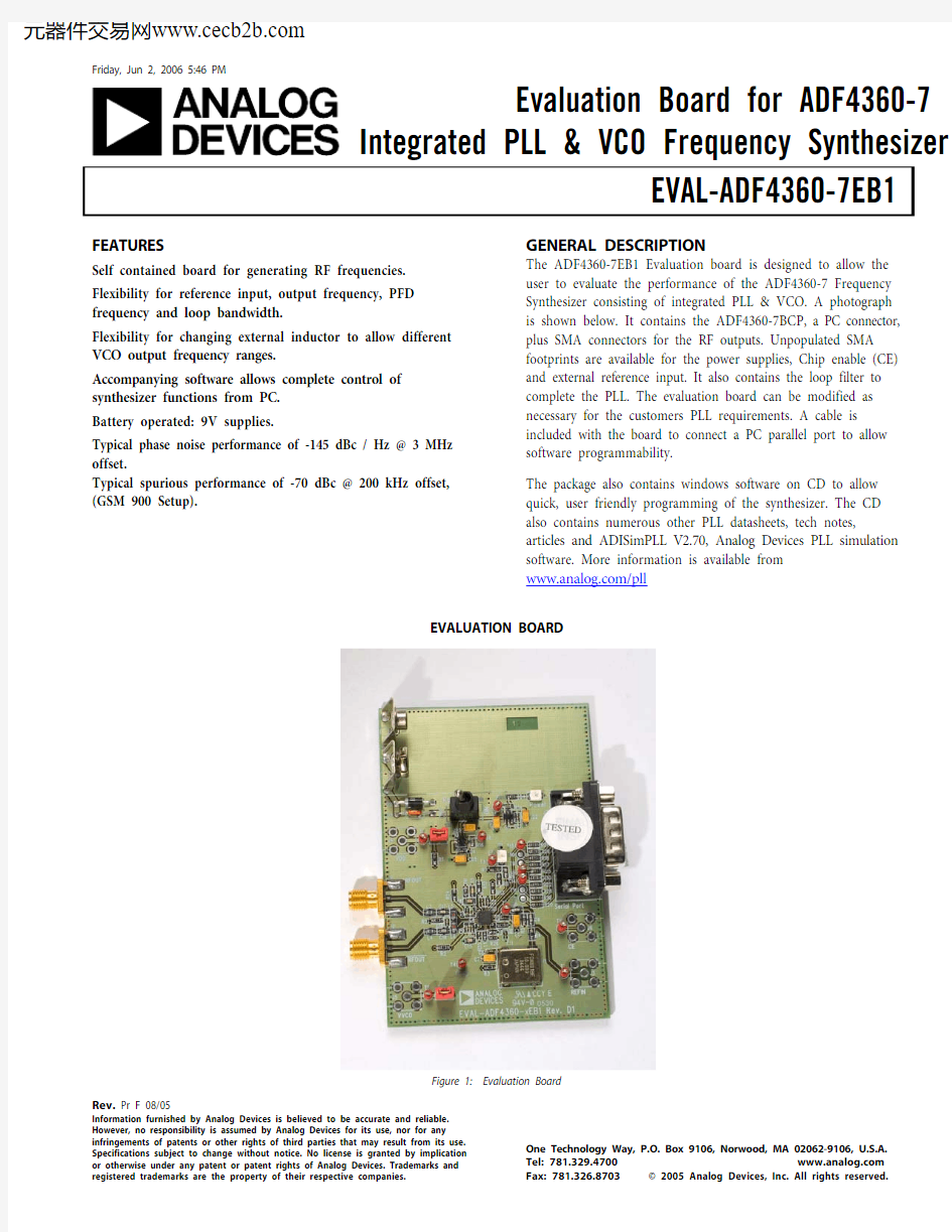
The ADF4360-7EB1 Evaluation board is designed to allow the user to evaluate the performance of the ADF4360-7 Frequency Synthesizer consisting of integrated PLL & VCO. A photograph is shown below. It contains the ADF4360-7BCP , a PC connector, plus SMA connectors for the RF outputs. Unpopulated SMA footprints are available for the power supplies, Chip enable (CE) and external reference input. It also contains the loop filter to complete the PLL. The evaluation board can be modified as necessary for the customers PLL requirements. A cable is included with the board to connect a PC parallel port to allow software programmability.
The package also contains windows software on CD to allow
quick, user friendly programming of the synthesizer. The CD also contains numerous other PLL datasheets, tech notes,
articles and ADISimPLL V2.70, Analog Devices PLL simulation software. More information is available from https://www.360docs.net/doc/d62726516.html,/pll
EVALUATION BOARD
Figure 1: Evaluation Board
EVAL-ADF4360-7EB1
Rev. Pr F | Page 2 of 7
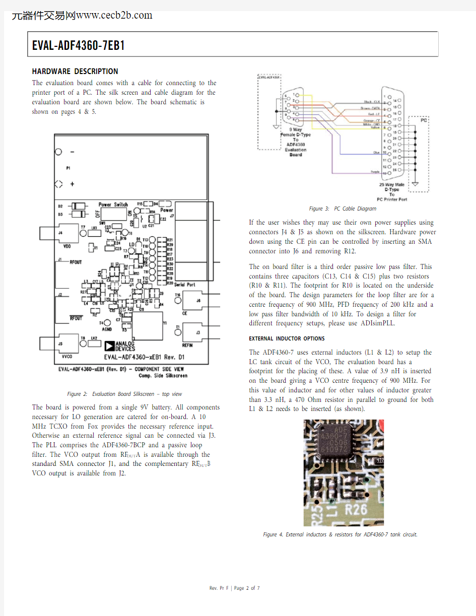
HARDWARE DESCRIPTION
The evaluation board comes with a cable for connecting to the printer port of a PC. The silk screen and cable diagram for the evaluation board are shown below. The board schematic is
shown on pages 4 & 5.
Figure 2: Evaluation Board Silkscreen – top view
The board is powered from a single 9V battery. All components necessary for LO generation are catered for on-board. A 10 MHz TCXO from Fox provides the necessary reference input. Otherwise an external reference signal can be connected via J3. The PLL comprises the ADF4360-7BCP and a passive loop filter. The VCO output from RF OUT A is available through the standard SMA connector J1, and the complementary RF OUT B VCO output is available from J2.
Figure 3: PC Cable Diagram
If the user wishes they may use their own power supplies using connectors J4 & J5 as shown on the silkscreen. Hardware power down using the CE pin can be controlled by inserting an SMA connector into J6 and removing R12.
The on board filter is a third order passive low pass filter. This contains three capacitors (C13, C14 & C15) plus two resistors (R10 & R11). The footprint for R10 is located on the underside of the board. The design parameters for the loop filter are for a centre frequency of 900 MHz, PFD frequency of 200 kHz and a low pass filter bandwidth of 10 kHz. To design a filter for different frequency setups, please use ADIsimPLL.
EXTERNAL INDUCTOR OPTIONS
The ADF4360-7 uses external inductors (L1 & L2) to setup the LC tank circuit of the VCO, The evaluation board has a
footprint for the placing of these. A value of 3.9 nH is inserted on the board giving a VCO centre frequency of 900 MHz. For this value of inductor and for other values of inductor greater than 3.3 nH, a 470 Ohm resistor in parallel to ground for both
L1 & L2 needs to be inserted (as shown).
Figure 4. External inductors & resistors for ADF4360-7 tank circuit.
EVAL-ADF4360-7EB1
Rev. Pr F | Page 3 of 7
To find the optimum frequency range for a given inductor, please consult the graph below. Simply ensure the desired
frequency is between the two lines and read off the appropriate inductance needed.
300
5004001200
130014001000110080090060070015000
5
10152030
25
EXT INDUCTANCE (nH)
F R E Q U E N C Y (M H z )
04441-028
Figure x: Output Center Frequency vs. External Inductor Value
RF OUTPUT STAGES
The output stage of the board allows the user to insert a tuned load for the particular frequency. The particular network
inserted in the board is optimized for 900 MHz operation. For different frequencies, the output stage needs different component values. Consult the datasheet for further
information. If in doubt use a 50 Ohm resistor instead of the shunt inductor, a 100 pF bypass capacitor and a zero ohm
resistor instead of the series inductor. It is very important that the same components be placed on the RF OUT A and RF OUT B lines , also it is essential that BOTH outputs be terminated with 50 Ohm loads. Otherwise the output power will not be optimum, and in some cases the part may malfunction.
EVAL-ADF4360-7EB1
Rev. Pr F | Page 4 of 7
Figure 8. EVAL-ADF4360-7EB1 Circuit Diagram
EVAL-ADF4360-7EB1
Figure 10. EVAL-ADF4360-7EB1 Circuit Diagram
Rev. Pr F | Page 5 of 7
EVAL-ADF4360-7EB1
Rev. Pr F | Page 6 of 7
SOFTWARE DESCRIPTION
The ADF4360-x software comes on a bundled installation CD. This is suitable for all the ADF4360-x devices. To install, simply double click on setup.exe and the install wizard installs the software, (Please note, administrator access on the PC is required to install the software) Follow the on-screen
instructions. The software will be installed in a default directory called “C:/Program Files/Analog Devices/ADF4360”. To run the software from this directory simply double click on ADF4360.exe.
Before the main software screen appears, the device window appears, which will ask the user to choose which device is being evaluated. Choose the appropriate version of the ADF4360 and click OK. The main interface window should now appear, (figure x).
PROGRAMMABLE SOFTWARE SETTINGS
Click on RF VCO Output Frequency, and the Output Frequency window will appear. Enter the desired PFD
frequency (in kHz) and click OK. Click on Reference frequency and insert the desired frequency in MHz. To modify charge pump setting 1 or 2, simply click over the text and the eight programmable settings for each will appear and can be modified. In a similar fashion the pre-scaler settings can be changed.
It may be necessary to adjust the core power level and the
output power setting to give optimum operation. These settings are clearly marked in the window below.
Click on RF PD Polarity button to set the PD polarity bit positive, this ensures all registers are loaded.
The part should now be setup, and other features can now be modified by the user. To examine the contents written to each register, the registers button can be selected. This also shows the hexadecimal number written to each register. As stated on the parts datasheet, the correct sequence of register writes is to the R counter, The Control latch and finally the N counter. Please note that a small delay needs to be maintained between programming the Control latch and the N counter
Figure 11. Software Front Panel Display
EVAL-ADF4360-7EB1 TABLE 1: BILL OF MATERIALS FOR EVAL-ADF4360-7EB1:
Rev. Pr F | Page 7 of 7