国显最新KD070D10-50NB-B5 SPEC(20121112)
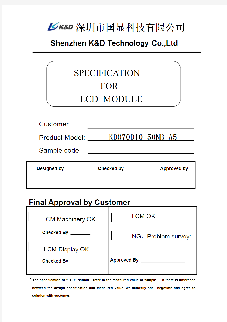
深圳市国显科技有限公司Shenzhen K&D Technology Co.,Ltd
SPECIFICATION
FOR
LCD MODULE
Customer:
Product Model:KD070D10-50NB-A5
Sample code:
Designed by Checked by Approved
by Array
※The specification of“TBD”should refer to the measured value of sample.If there is difference between the design specification and measured value,we naturally shall negotiate and agree to
Revision History
Contents
1Numbering System
——
(1)(2)(3)(4)(5)(6)(7)(8)
No Definition Specifications
(1)TFT LCM Productor
No.
KD----Kingdisplay technologiy Co.,Ltd
(2)Display monitor
opposite angle line size
Unit:mm or mmm(size<10inch:takes two
integers;size>=10inch:takes three integers)
(3)Productor Types D----Digital photo frame/DVD G----GPS
M----MP
P----Mobil-Phone
(4)Productor Development
Series No.By two figures characters expression from01to 99
(5)Interface PIN Number By two figures characters expression from01to
99
(6)With Touch Panel Or
Not
T----With T/P;N----Without T/P
(7)LCD Type A----AUO;M----CMO;C----CPT;B----BOE;
L----LG;W----Wintek;H----HSD;T----Tianma;
Y----Hydis;I----INNOLUX;S----Sharp
(8)Productor Development
edition No.
By The English litters:A1~Z9
2Scope
This specification applies to the TFT LCD module which is designed and manufactured by LCM Factory of Shenzhen K&D Technology Co.,Ltd.
3Normative Reference
GB/T4619-1996《Liquid Crystal Display Test Method》
GB/T2424《Basic environmental Testing Procedures for Electric and Electronic Products.》
GB/T2423《Basic Testing Procedures for Electric and Electronic Products》IEC61747-1《SIXTH PARTGB2828`2829-87《National Standard of PRC》
4Definitions
4.1Definitions of Vop
The definitions of threshold voltage Vth1,Vth2the following typical waveforms are applied on liquid crystal by the method of equalized voltage for each duty and bias.
【selected waveform】【non-selected waveform】
①Vth1:The voltage which the brightness of segment indicates50%of saturated value on the conditions of selected waveform
(f f=80Hz,Φ=10°θ=270°at25℃)
②Vth2:The voltage which the brightness of segment indicates50%of saturated value on the conditions of non-selected waveform
(f f=80Hz,Φ=10°θ=270°at25℃)
③Vop:(Vth1(50%)+Vth2(50%))/2(f f=80Hz,Φ=10°θ=270°at25℃)
4.2Definition of Response Time Tr,Td
①Tr:The time required which the brightness of segment
becomes10%from100%when waveform is switched to
selected one from non-selected one.(f f=80Hz,Φ=10°
θ=270°at25℃)
becomes 90%from 10%when waveform is switched to selected one from selected one.(f f =80Hz,Φ=10°θ=270°at 25℃)
4.3Definition of Contrast Ratio Cr
Cr=A/B
1A:Segments brightness in case of non-selected waveform 2B:Segments
brightness in case of selected waveform 4.4Definition of Angle and Viewing Range
Angular Graph:Constrast Ratio
Such as:
Viewing Angle Range:
80(Cr>2)Horizontal 70(Cr>2)Vertical
5Technology Specifications
5.1Feature
This single-display module is suitable for use in Multidedia Player products. The LCD adopts one backlight with High brightness18-lamps white LED.
1)Construction:7〞а-Si color TFT-LCD,White LED backlight and FPC.
2)LCD:
2.1Amorphous-TFT7-inch display,transmissive,normally white type.
2.2800(RGB)×480dots Matrix.
2.3Narrow-contact ledge technique.
3)RGB interface.
4)Video signal interface:Parallel RGB.
5.2Mechanical Specifications
Item Specifications Unit Dimensional outline164.9(W)×100.0(H)×3.4(D)mm Active area154.08(W)×85.92(H)mm
Pixel size63.2(W)×RGB×179(H)um
Resolution800(RGB)×480pixel
Luminance250(TYP)cd/m2 5.3Absolute Max.Rating
Item Symbol
Values
Unit Remark Min.Max
Power voltage DV DD-0.5 5.0V AV DD-0.515V V GH-0.340V V GL-200.3V
Operation temperature T OP-1060℃
Storage temperature T ST-2070℃
Note:The absolute maximum rating values of this product not allowed to be exceeded at any times.Should be module be used with any of absolute maximum ratings exceeded.The characteristics of the module may not be recovered,or in an extreme case,the module may be permanently destroyed.
5.4Electrical Characteristics Note1
Item Symbol
Values
Unit Remark Min.Typ Max
Power voltage DV DD 3.0 3.3 3.6V Note2 AV DD10.110.310.5V
V GH17.51818.5V
V GL-8.5-8-7.5V
Input signal voltage V COM 3.1 3.8 3.4V
Input logic high voltage V IH0.7DV DD-DV DD V
Note3 Input logic low voltage V IL0-0.3DV DD V
Note1:Be sure to apply DV DD and V GL to the LCD first,and then apply V GH. Note2:DV DD setting should match the signals output voltage(refer to Note3)of Customer’s system board.
Note3:DCLK,HS.VS,RESET,U/D,L/R,DE,R0-R7,G0-G7,G0-G7,MODE,DITHB.
Test Conditions:
1.DVDD=3.3V,I LED=120mA,the ambient temperature is25℃.
2.The test systems refer to Note2.
Note 1:Definition of viewing angle range
Note 2:Definition of optical measurement system.
The optical characteristics should be measured in dark room.After 30minutes operation,the optical properties are measured at the center point of the LCD screen.(Viewing angle is measured by ELDIM-EZ contrast/Height :1.2mm ,Response time is measured by Photo detector TOPCON BM-7,other items are measured by BM-5A/Field of view:1°/Height:500mm.)
Normal line
Φ=270°
6o’clock direction
Φ=0°
Φ=180°
Φ=270°
6o’clock direction
Φ=0°
Φ=180°
Normal line θ=Φ=0°
Note 3:Definition of Response time
The response time is defined as the LCD optical switching time interval between “White”state and “Black”state.Rise time (T ON )is the time between photo detector output intensity changed from 90%to 10%.And fall time (T OFF )is the time between photo detector output intensity changed from 10%to 90%.
100%90%
10%0%
P h o t o d e t e c t o r o u t p u t (R e l a t i v e v a l u e )
ON
White (TFT OFF)
Black (TFT ON)
White (TFT OFF)
Note 4:Definition of contrast ratio
state
Black"" the on LCD when measured Luminance state White"" the on LCD when measured Luminance (CR) ratio Contrast =
Note 5:Definition of color chromaticity (CIE1931)
Color coordinates measured at center point of LCD.
Note 6:All input terminals LCD panel must be ground while measuring the center
area of the panel.The LED driving condition is I LED =180mA.Note 7:Definition of Luminance Uniformity
Active area is divided into 9measuring areas.Every measuring point is placed at the center of each measuring area.
max
min
B B
(Yu)Uniformity Luminance =L-------Active area length W-----Active area width
B max :The measured maximum luminance of all measurement position.
B min :The measured minimum luminance of all measurement position.
5.6LED back light specification(18White Chips)
Item Symbol Condition Min Typ Max Unit Forward Voltage Vf lf=120mA99.69.9V Uniformity(with L/G)ΔB p lf=120mA80--%
5.7Interface Pin Connections
21G6I Green data
22G5I Green data
23G4I Green data
24G3I Green data
25G2I Green data
26G1I Green data Note2
27G0I Green data(LSB)Note2
28R7I Red data(MSB)
29R6I Red data
30R5I Red data
31R4I Red data
32R3I Red data
33R2I Red data
34R1I Red data Note2
35R0I Red data(LSB)Note2
36GND P Power Ground
37DCLK I Sample clock Note3
38GND P Power Ground
39L/R I Left/right selection Note4,5
40U/D I Up/down selection Note4,5
41V GH P Gate ON Voltage
42V GL P Gate OFF Voltage
43AV DD P Power for Analog Circuit
44RESET I Global reset pin.Note6
45NC-No connection
46V COM I Common Voltage
47DITHB I Dithering function Note7
48GND P Power Ground
49NC-No connection
50NC-No connection
I:input,O:output,P:Power
Note1:DE/SYNC mode select.Normally pull high.
When select DE mode,MODE=”1”,VS and HS must pull high.
When select SYNC mode,MODE=”0”,DE must be grounded.
Note2:When input18bits RGB data,the two low bits of R,G and B data must be grounded.
Note 3:Data shall be latched at the falling edge of DCLK.Note 4:Selection of scanning mode
Setting of scan control input
Scanning direction U/D L/R GND DV DD Up to down,left to right DV DD GND
Down
to up,right to left
GND GND Up to down,right
to left DV DD
DV DD
Down to up,left to right
Note 5:Definition of scanning direction.
Refer to the figure as below:
Note 6:Global reset pin.Suggest to connect with
an RC reset circuit for stability.Normally pull high.Note 7:Dithering function enable control,normally pull high.
When DITHB=”1”,Disable internal dithering function,When DITHB=”0”,Enable internal dithering function,
6Signal timing diagram
6.2Signal Timing Diagram
6.2.1Power ON/OFF Sequence
a Power on
b Power off
6.2.2Data input format
6.2.3Timing Diagram
7Reliability Test Conditions And Methods
8Inspection standard
x
x
Intensity Of
Adhesion
If lower than specification,reject Gold Fold Twist Reject
07IC/FPC
Bonding
Silicon
According to outline,no gold outside,
seal can not be higher than LCD
FPC Gold Sever
Reject
08SMT
Lack of
Component、
Polarity Inverse
If exist,reject
Leak Solder、
Virtual Solder
If exist,reject
Short Circuit In
Solder Point
If exist,reject
Tin Ball If exist,reject
Tin Acumination If visual,reject
Height
Solder Point If higher0.5mm than component.reject
Height of
component
Either side higher0.5mm than
component,reject