SC1142DG datasheet
SC1142
https://www.360docs.net/doc/dd11102385.html, September 2012
Energy-Efficient, Accurate Primary-Side Regulation CV/CC Switcher for Adapters and Chargers
Output Power Table
Product
3
85-265 VAC
Adapter 15.5 W Open Frame 2
6.1 W SC1142
P/N Suffix
Cable Drop Compensation (Ratio to No-load Voltage
Regulation)
D0 1.01D1 1.02D2 1.04D3
1.06
Table 1. Output Power Table. Notes:
1. Minimum continuous power in a typical non-ventilated enclosed adapter measured at +50 °C ambient, device T J ≤ 100 °C.
2. Maximum practical continuous power in an open frame design with adequate heat sinking, measured at +50 °C.
3. Package: D: SO-8C.
Product Highlights
Dramatically Simplifies CV/CC Converters
? Eliminates optocoupler and all secondary CV/CC control circuitry
? Eliminates all control loop compensation circuitry
Advanced Performance Features
? Compensates for transformer inductance tolerances ? Compensates for input line voltage variations ? Compensates for cable voltage drop
? Compensates for external component temperature variations ? Very tight IC parameter tolerances using proprietary trimming technology
? Frequency jittering greatly reduces EMI filter cost
? Even tolerances achievable with external resistor selection/trimming
? Programmable switching frequency up to 85 kHz to reduce transformer size
? Minimum operation frequency of ~1.4 kHz improves transient load response Advanced Protection/Safety Features
? Auto-restart protection reduces power delivered by >90% for output short circuit and control loop faults (open and shorted components)
? Hysteretic thermal shutdown – automatic recovery reduces power supply returns from the field
? Meets high-voltage creepage requirements between DRAIN and all other pins both on the PCB and at the package EcoSmart ? – Energy Efficient
? Easily meets all global energy efficiency regulations with no added components
? No-load consumption <30 mW at 230 VAC input with bias winding
? ON/OFF control provides constant efficiency down to very light loads – ideal for CEC regulations
? No current sense resistors – maximizes efficiency Green Package
? Halogen free and RoHS compliant package
Applications
? Chargers for cell/cordless phones, PDAs, MP3/portable audio devices, adapters, etc.
Description
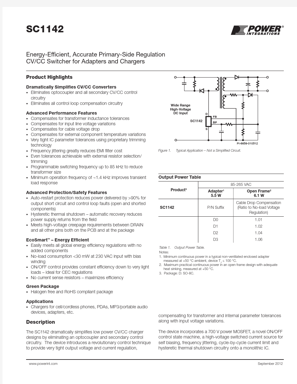
The SC1142 dramatically simplifies low power CV/CC charger designs by eliminating an optocoupler and secondary control circuitry. The device introduces a revolutionary control technique to provide very tight output voltage and current regulation,
Figure 1. Typical Application – Not a Simplified Circuit.
compensating for transformer and internal parameter tolerances along with input voltage variations.
The device incorporates a 700 V power MOSFET, a novel ON/OFF control state machine, a high-voltage switched current source for self biasing, frequency jittering, cycle-by-cycle current limit and hysteretic thermal shutdown circuitry onto a monolithic IC.
https://www.360docs.net/doc/dd11102385.html,
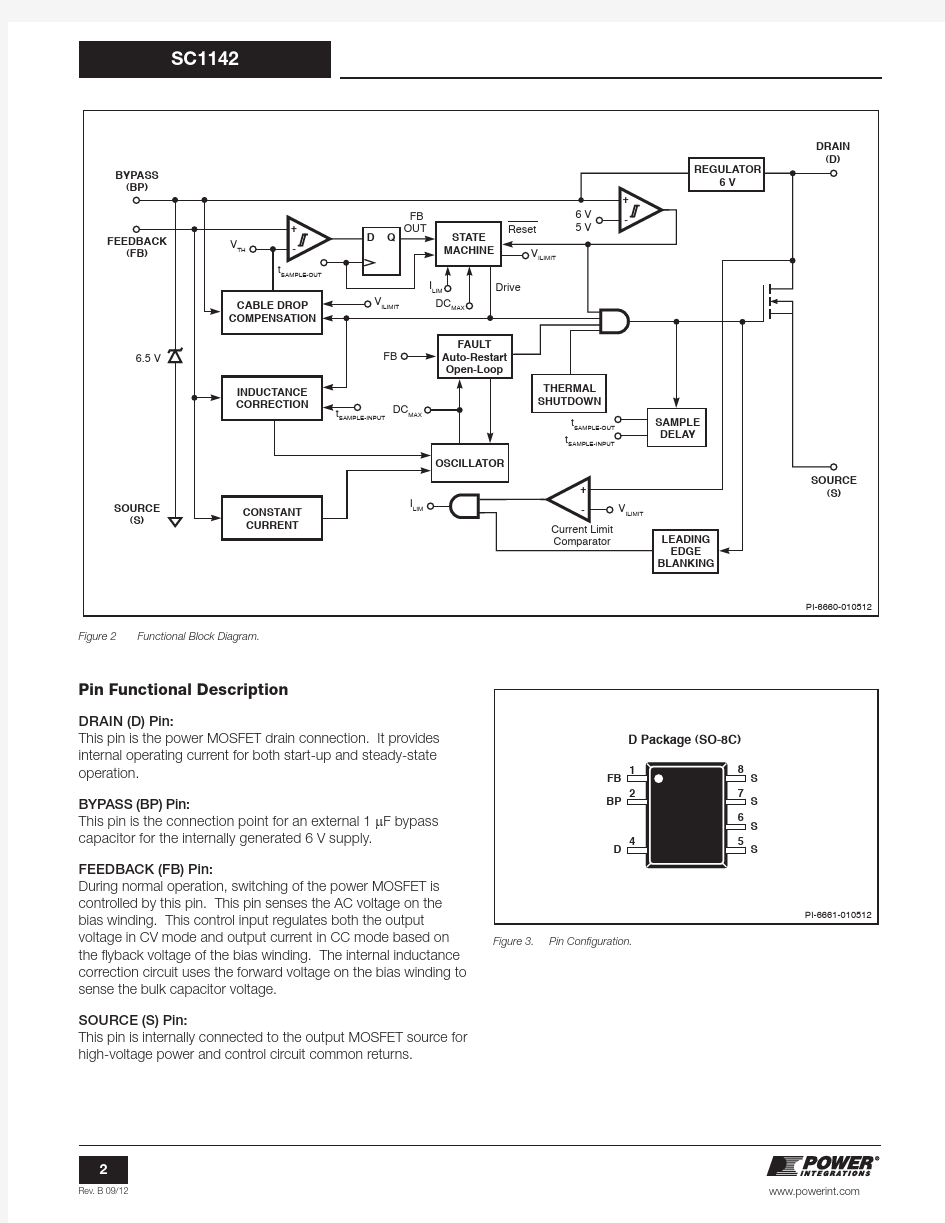
Pin Functional Description
DRAIN (D) Pin:
This pin is the power MOSFET drain connection. It provides internal operating current for both start-up and steady-state operation.
BYPASS (BP) Pin:
This pin is the connection point for an external 1 m F bypass capacitor for the internally generated 6 V supply.
FEEDBACK (FB) Pin:
During normal operation, switching of the power MOSFET is controlled by this pin. This pin senses the AC voltage on the bias winding. This control input regulates both the output voltage in CV mode and output current in CC mode based on the flyback voltage of the bias winding. The internal inductance correction circuit uses the forward voltage on the bias winding to sense the bulk capacitor voltage.
SOURCE (S) Pin:
This pin is internally connected to the output MOSFET source for high-voltage power and control circuit common returns.
Figure 2 Functional Block Diagram.
Figure 3. Pin Configuration.
https://www.360docs.net/doc/dd11102385.html,
SC1142 Functional Description
The SC1142 combines a high-voltage power MOSFET switch with a power supply controller in one device. Similar to the LinkSwitch-LP and TinySwitch-III it uses an ON/OFF control to regulate the output voltage. In addition, the switching frequency is modulated to regulate the output current to provide a constant current characteristic. The SC1142 controller consists of an oscillator, feedback (sense and logic) circuit, 6 V regulator, over-temperature protection, frequency jittering, current limit circuit, leading-edge blanking, inductance correction circuitry, frequency control for constant current regulation and on/off state machine for CV control.
Inductance Correction Circuitry
If the primary magnetizing inductance is either too high or low the converter will automatically compensate for this by adjusting the oscillator frequency. Since this controller is designed to operate in discontinuous-conduction mode the output power is directly proportional to the set primary inductance and its
tolerance can be completely compensated with adjustments to the switching frequency.
Constant Current (CC) Operation
As the output voltage and therefore the flyback voltage across the bias winding ramps up, the FEEDBACK pin voltage increases. The switching frequency is adjusted as the FEEDBACK pin voltage increases to provide a constant output current regulation. The constant current circuit and the inductance correction circuit are designed to operate concurrently in the CC region. Constant Voltage (CV) Operation
As the FEEDBACK pin approaches 2 V from the constant current regulation mode, the power supply transitions into CV operation. The switching frequency at this point is at its
maximum value, corresponding to the peak power point of the CV/CC characteristic. The controller regulates the FEEDBACK pin voltage to remain at FEEDBACK pin threshold (V FBTH ) using an on/off state-machine. The FEEDBACK pin voltage is
sampled 2.5 m s after the turn-off of the high-voltage switch. At light loads the current limit is also reduced to decrease the transformer flux density and the FEEDBACK pin sampling is done earlier.
Output Cable Compensation
This compensation provides a constant output voltage at the end of the cable over the entire load range in CV mode. As the converter load increases from no-load to the peak power point (transition point between CV and CC) the voltage drop introduced across the output cable is compensated by increasing the FEEDBACK pin reference voltage. The controller determines the output load and therefore the correct degree of compensation based on the output of the state machine. The amount of cable drop compensation is determined by the part suffix number as shown in the front page of the data sheet.
Auto-Restart and Open-Loop Protection
In the event of a fault condition such as an output short or an open loop condition the SC1142 enters into an appropriate protection mode as described below.
In the event the FEEDBACK pin voltage during the flyback
period falls below 0.7 V before the FEEDBACK pin sampling delay (~2.5 m s) for a duration in excess of ~450 ms (auto-restart on-time (t AR-ON ) the converter enters into auto-restart, wherein the power MOSFET is disabled for 1.2 seconds. The auto-restart alternately enables and disables the switching of the power MOSFET until the fault condition is removed.
In addition to the conditions for auto-restart described above, if the sensed FEEDBACK pin current during the forward period of the conduction cycle (switch “on” time) falls below 120 m A, the converter annunciates this as an open-loop condition (top resistor in potential divider is open or missing) and reduces the auto-restart time from 450 ms to approximately 6 clock cycles (90 m s), whilst keeping the disable period of 2 seconds. Over-Temperature Protection
The thermal shutdown circuitry senses the die temperature. The threshold is set at 142 °C typical with a 60 °C hysteresis. When the die temperature rises above this threshold (142 °C) the power MOSFET is disabled and remains disabled until the die temperature falls by 60 °C, at which point the MOSFET is re-enabled.
Current Limit
The current limit circuit senses the current in the power MOSFET. When this current exceeds the internal threshold (I LIMIT ), the power MOSFET is turned off for the remainder of that cycle. The leading edge blanking circuit inhibits the current limit comparator for a short time (t LEB ) after the power MOSFET is turned on. This leading edge blanking time has been set so that current spikes caused by capacitance and rectifier reverse recovery time will not cause premature termination of the MOSFET conduction. The SC1142 also contains a “di/dt” correction feature to minimize CC variation across the input line range.
6 V Regulator
The 6 V regulator charges the bypass capacitor connected to the BYPASS pin to 6 V by drawing a current from the voltage on the DRAIN, whenever the MOSFET is off. The BYPASS pin is the internal supply voltage node. When the MOSFET is on, the device runs off of the energy stored in the bypass capacitor. Extremely low power consumption of the internal circuitry allows the SC1142 to operate continuously from the current drawn from the DRAIN pin. A bypass capacitor value of 1 m F is
sufficient for both high frequency decoupling and energy storage.
https://www.360docs.net/doc/dd11102385.html,
Absolute Maximum Ratings (1,5)
DRAIN Voltage .................................. .......................-0.3 V to 700 V DRAIN Peak Current: .................................................654 mA Peak Negative Pulsed Drain Current ................... .........-100 mA (2) FEEDBACK Voltage ................................................... ...-0.3 V to 9 V FEEDBACK Current .................................................... .........100 mA BYPASS Pin Voltage ...................................... .............-0.3 V to 9 V Storage Temperature ...........................................-65 °C to 150 °C Operating Junction Temperature..................... ...-40 °C to 150 °C Lead Temperature (4) ....................................................... .........260 °C
Notes:
1. All voltages referenced to SOURCE, T A = 25 °C.
2. Duration not to exceed 2 ms.
3. 1/16 in. from case for 5 seconds.
4. M aximum ratings specified may be applied, one at a time without causing permanent damage to the product. Exposure to Absolute Maximum ratings for extended periods of time may affect product reliability.
Thermal Impedance
Thermal Impedance: D Package:
(q JA ) ..................................100 °C/W (2); 80 °C/W (3)
(q JC )(1) .........................................................30 °C/W
Notes:
1. Measured on pin 8 (SOURCE) close to plastic interface.
2. Soldered to 0.36 sq. in. (232 mm 2), 2 oz. (610 g/m 2) copper clad.
3. Soldered to 1 sq. in. (645 mm 2), 2 oz. (610 g/m 2) copper clad.
https://www.360docs.net/doc/dd11102385.html,
https://www.360docs.net/doc/dd11102385.html,
NOTES:
1. Auto-restart ON-time is a function of switching frequency programmed by t on x I FB and minimum frequency in CC mode.
2. The current limit threshold is compensated to cancel the effect of current limit delay. As a result the output current stays constant
across the input line range.3. I DSS1 is the worst case OFF state leakage specification at 80% of BV DSS and maximum operating junction temperature. I DSS2 is a
typical specification under worst case application conditions (rectified 265 VAC) for no-load consumption calculations.4. When the duty-cycle exceeds DC MAX the SC1142 operates in on-time extension mode.5. This parameter is derived from characterization.
6. At light load the current limit is reduced to ~32% and t FB at ~1.8 m s typical.
https://www.360docs.net/doc/dd11102385.html,
For the latest updates, visit our website: https://www.360docs.net/doc/dd11102385.html,
Power Integrations reserves the right to make changes to its products at any time to improve reliability or manufacturability. Power Integrations does not assume any liability arising from the use of any device or circuit described herein. POWER INTEGRATIONS MAKES NO WARRANTY HEREIN AND SPECIFICALLY DISCLAIMS ALL WARRANTIES INCLUDING, WITHOUT LIMITATION, THE IMPLIED WARRANTIES OF MERCHANTABILITY, FITNESS FOR A PARTICULAR PURPOSE, AND NON-INFRINGEMENT OF THIRD PARTY RIGHTS. Patent Information
The products and applications illustrated herein (including transformer construction and circuits external to the products) may be covered by one or more U.S. and foreign patents, or potentially by pending U.S. and foreign patent applications assigned to Power Integrations. A complete list of Power Integrations patents may be found at https://www.360docs.net/doc/dd11102385.html,. Power Integrations grants its customers a license under certain patent rights as set forth at https://www.360docs.net/doc/dd11102385.html,/ip.htm.
Life Support Policy
POWER INTEGRATIONS PRODUCTS ARE NOT AUTHORIZED FOR USE AS CRITICAL COMPONENTS IN LIFE SUPPORT DEVICES OR SYSTEMS WITHOUT THE EXPRESS WRITTEN APPROVAL OF THE PRESIDENT OF POWER INTEGRATIONS. As used herein:
1. A Life support device or system is one which, (i) is intended for surgical implant into the body, or (ii) supports or sustains life, and (iii)
whose failure to perform, when properly used in accordance with instructions for use, can be reasonably expected to result in significant injury or death to the user.
2. A critical component is any component of a life support device or system whose failure to perform can be reasonably expected to cause
the failure of the life support device or system, or to affect its safety or effectiveness.
The PI logo, TOPSwitch, TinySwitch, LinkSwitch, LYTSwitch, DPA-Switch, PeakSwitch, CAPZero, SENZero, LinkZero, HiperPFS, HiperTFS, HiperLCS, Qspeed, EcoSmart, Clampless, E-Shield, Filterfuse, StakFET, PI Expert and PI FACTS are trademarks of Power Integrations, Inc. Other trademarks are property of their respective companies. ?2012, Power Integrations, Inc.
Power Integrations Worldwide Sales Support Locations
World Headquarters
5245 Hellyer Avenue
San Jose, CA 95138, USA. Main: +1-408-414-9200 Customer Service:
Phone: +1-408-414-9665 Fax: +1-408-414-9765
e-mail: usasales@https://www.360docs.net/doc/dd11102385.html,
China (Shanghai)
Rm 1601/1610, Tower 1,
Kerry Everbright City
No. 218 Tianmu Road West, Shanghai, P.R.C. 200070 Phone: +86-21-6354-6323 Fax: +86-21-6354-6325
e-mail: chinasales@https://www.360docs.net/doc/dd11102385.html,
China (ShenZhen)
3rd Floor, Block A,
Zhongtou International Business Center, No. 1061, Xiang Mei Rd, FuTian District, ShenZhen, China, 518040
Phone: +86-755-8379-3243 Fax: +86-755-8379-5828
e-mail: chinasales@https://www.360docs.net/doc/dd11102385.html, Germany
Lindwurmstrasse 114
80337 Munich
Germany
Phone: +49-895-527-39110
Fax: +49-895-527-39200
e-mail: eurosales@https://www.360docs.net/doc/dd11102385.html,
India
#1, 14th Main Road
Vasanthanagar
Bangalore-560052 India
Phone: +91-80-4113-8020
Fax: +91-80-4113-8023
e-mail: indiasales@https://www.360docs.net/doc/dd11102385.html,
Italy
Via Milanese 20, 3rd. Fl.
20099 Sesto San Giovanni (MI)
Italy
Phone: +39-024-550-8701
Fax: +39-028-928-6009
e-mail: eurosales@https://www.360docs.net/doc/dd11102385.html,
Japan
Kosei Dai-3 Bldg.
2-12-11, Shin-Yokomana,
Kohoku-ku
Yokohama-shi Kanagwan
222-0033 Japan
Phone: +81-45-471-1021
Fax: +81-45-471-3717
e-mail: japansales@https://www.360docs.net/doc/dd11102385.html,
Korea
RM 602, 6FL
Korea City Air T erminal B/D, 159-6
Samsung-Dong, Kangnam-Gu,
Seoul, 135-728, Korea
Phone: +82-2-2016-6610
Fax: +82-2-2016-6630
e-mail: koreasales@https://www.360docs.net/doc/dd11102385.html,
Singapore
51 Newton Road
#15-08/10 Goldhill Plaza
Singapore, 308900
Phone: +65-6358-2160
Fax: +65-6358-2015
e-mail: singaporesales@https://www.360docs.net/doc/dd11102385.html,
Taiwan
5F, No. 318, Nei Hu Rd., Sec. 1
Nei Hu Dist.
Taipei, Taiwan 114, R.O.C.
Phone: +886-2-2659-4570
Fax: +886-2-2659-4550
e-mail: taiwansales@https://www.360docs.net/doc/dd11102385.html,
Europe HQ
1st Floor, St. James’s House
East Street, Farnham
Surrey GU9 7TJ
United Kingdom
Phone: +44 (0) 1252-730-141
Fax: +44 (0) 1252-727-689
e-mail: eurosales@https://www.360docs.net/doc/dd11102385.html,
Applications Hotline
World Wide +1-408-414-9660
Applications Fax
World Wide +1-408-414-9760
Revision Notes Date
B Code A Release0912