IXTL2X180N10T;中文规格书,Datasheet资料
Symbol Test Conditions
Maximum Ratings
V DSS T J = 25°C to 175°C
100V V DGR T J = 25°C to 175°C, R GS = 1M Ω100V V GSS Continuous ± 20V V GSM Transient
± 30
V I D25T C = 25°C
100
A I L(RMS)External Lead Current Limit
75A I DM T C = 25°C, Pulse Width Limited by T JM 450
A I A T C = 25°C 25A E AS T C = 25°C 750mJ P D T C = 25°C
150
W
dv/dt I S ≤ I DM , V DD ≤ V DSS , T J ≤ 175°C 3 V/ns
T J -55 ... +175
°C T JM 175
°C T stg -55 ... +175
°C T L
1.6mm (0.062 in.) from Case for 10s 300°C T SOLD Plastic Body for 10s
260
°C F C
Mounting Force 20..120 /9..27 N/lb.
Weight
8
g
N-Channel Enhancement Mode Avalanche Rated
Fast Intrinsic Rectifier
V DSS = 100V I D25
= 2x100A R DS(on)
≤ 9m Ω
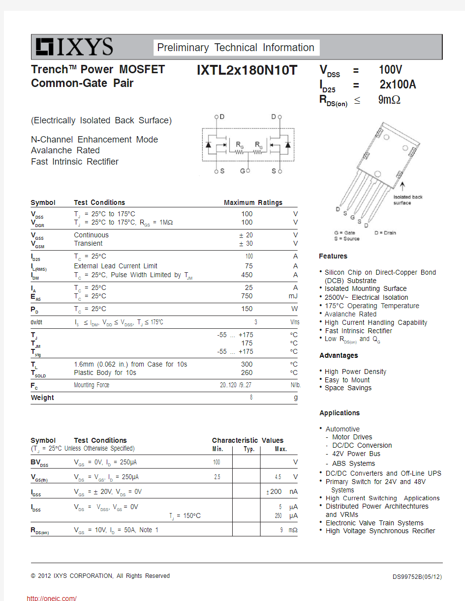
Trench TM Power MOSFET Common-Gate Pair
IXTL2x180N10T
(Electrically Isolated Back Surface)Symbol Test Conditions Characteristic Values (T J = 25°C Unless Otherwise Specified) Min. Typ. Max.BV DSS V GS = 0V, I D = 250μA 100V V GS(th)V DS = V GS , I D = 250μA 2.5 4.5V I GSS V GS = ± 20V, V DS = 0V
± 200
nA
I DSS V DS = V DSS , V GS = 0V
5 μA T J = 150°C 250 μ
A
R DS(on)
V GS = 10V, I D = 50A, Note 1
9 m
Ω
Features
z
Silicon Chip on Direct-Copper Bond (DCB) Substrate z
Isolated Mounting Surface z
2500V~ Electrical Isolation z
175°C Operating Temperature z
Avalanche Rated z
High Current Handling Capability z
Fast Intrinsic Rectifier z
Low R DS(on) and Q G
Advantages
z High Power Density z
Easy to Mount z
Space Savings
Applications
z
Automotive -Motor Drives
-DC/DC Conversion -42V Power Bus -ABS Systems z
DC/DC Converters and Off-Line UPS z
Primary Switch for 24V and 48V Systems z
High Current Switching Applications z
Distributed Power Architechtures and VRMs z
Electronic Valve Train Systems z
High Voltage Synchronous Recifier
IXYS Reserves the Right to Change Limits, Test Conditions, and Dimensions .
Symbol Test Conditions Characteristic Values
Source-Drain Diode
Symbol Test Conditions Characteristic Values (T J = 25°C, Unless Otherwise Specified) Min. Typ. Max.I S V GS = 0V
180 A I SM Repetitive, Pulse Width Limited by T JM 450 A V SD I F = 50A, V GS = 0V, Note 1
1.0 V
t rr
60 ns
I F = 25A, V GS = 0V -di/dt = 100A/μs, V R = 50V
Note 1. Pulse test, t ≤ 300μs, duty cycle, d ≤ 2%.
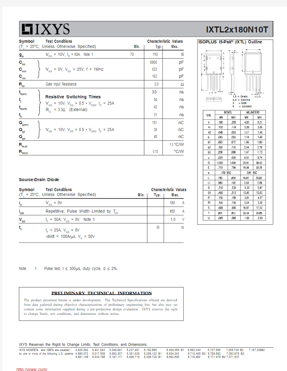
1,5 = Drain 2,4 = Source 3 = Gate 6 = Isolated
PRELIMINARY TECHNICAL INFORMATION
The product presented herein is under development. The Technical Specifications offered are derived from data gathered during objective characterizations of preliminary engineering lots; but also may yet contain some information supplied during a pre-production design evaluation. IXYS reserves the right to change limits, test conditions, and dimensions without notice.
分销商库存信息: IXYS
IXTL2X180N10T