641006-D51G06JA中文资料
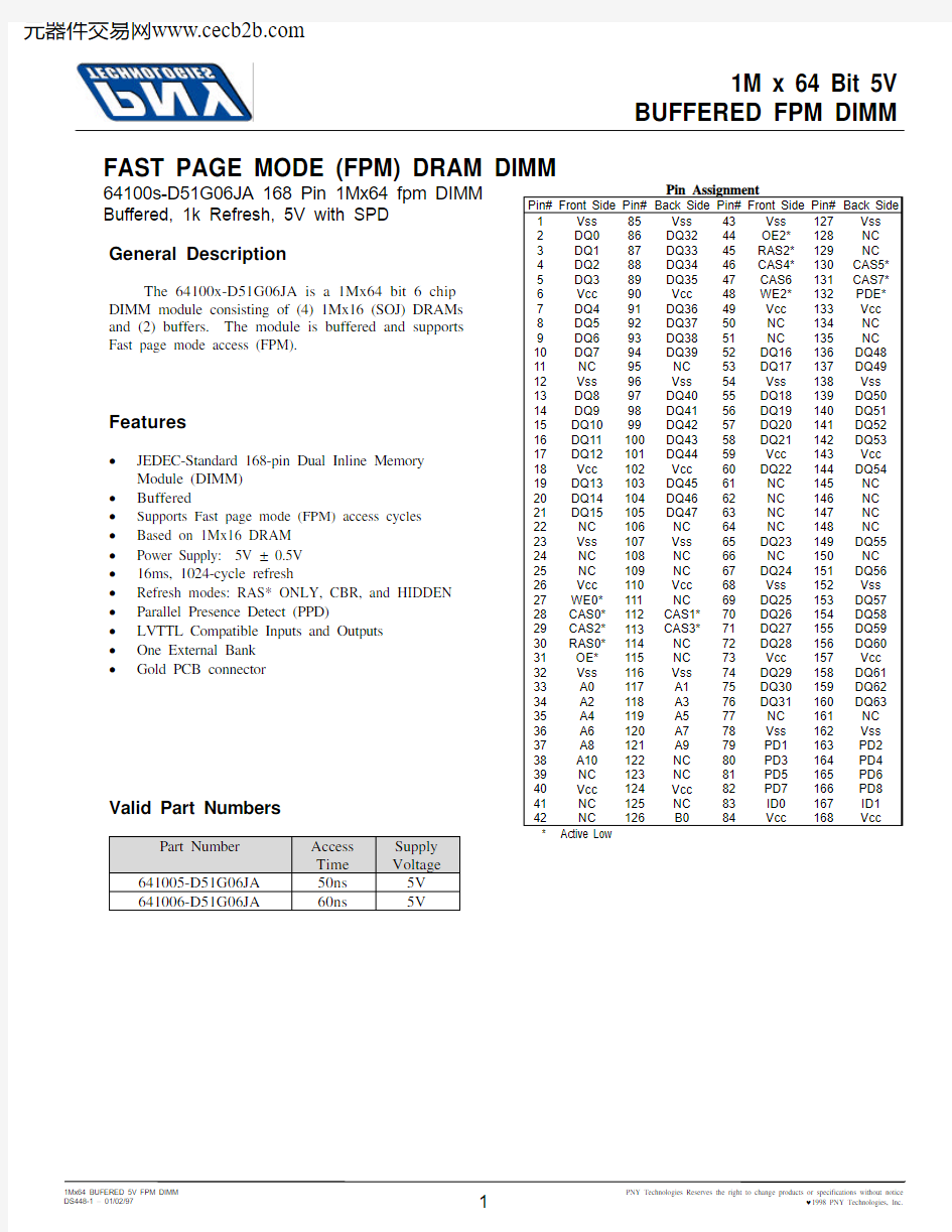
Pin Assignment
Pin#Front Side Pin#Back Side Pin#Front Side Pin#Back Side 1Vss 85Vss 43Vss 127Vss 2DQ086DQ3244OE2*128NC 3DQ187DQ3345RAS2*129NC 4DQ288DQ3446CAS4*130CAS5*5DQ389DQ3547CAS6131CAS7*6Vcc 90Vcc 48WE2*132PDE*7DQ491DQ3649Vcc 133Vcc 8DQ592DQ3750NC 134NC 9DQ693DQ3851NC 135NC 10DQ794DQ3952DQ16136DQ4811NC 95NC 53DQ17137DQ4912Vss 96Vss 54Vss 138Vss 13DQ897DQ4055DQ18139DQ5014DQ998DQ4156DQ19140DQ5115DQ1099DQ4257DQ20141DQ5216DQ11100DQ4358DQ21142DQ5317DQ12101DQ4459Vcc 143Vcc 18Vcc 102Vcc 60DQ22144DQ5419DQ13103DQ4561NC 145NC 20DQ14104DQ4662NC 146NC 21DQ15105DQ4763NC 147NC 22NC 106NC 64NC 148NC 23Vss 107Vss 65DQ23149DQ5524NC 108NC 66NC 150NC 25NC 109NC 67DQ24151DQ5626Vcc 110Vcc 68Vss 152Vss 27WE0*111NC 69DQ25153DQ5728CAS0*112CAS1*70DQ26154DQ5829CAS2*113CAS3*71DQ27155DQ5930RAS0*114NC 72DQ28156DQ6031OE*115NC 73Vcc 157Vcc 32Vss 116Vss 74DQ29158DQ6133A0117A175DQ30159DQ6234A2118A376DQ31160DQ6335A4119A577NC 161NC 36A6120A778Vss 162Vss 37A8121A979PD1163PD238A10122NC 80PD3164PD439NC 123NC 81PD5165PD640Vcc 124Vcc 82PD7166PD841NC 125NC 83ID0167ID142NC 126B084Vcc 168Vcc
* Active Low
FAST PAGE MODE (FPM) DRAM DIMM
64100s-D51G06JA 168 Pin 1Mx64 fpm DIMM Buffered, 1k Refresh, 5V with SPD Features
? JEDEC-Standard 168-pin Dual Inline Memory
Module (DIMM)? Buffered
? Supports Fast page mode (FPM) access cycles ? Based on 1Mx16 DRAM ? Power Supply: 5V ± 0.5V ? 16ms, 1024-cycle refresh
? Refresh modes: RAS* ONLY, CBR, and HIDDEN ? Parallel Presence Detect (PPD)
? LVTTL Compatible Inputs and Outputs ? One External Bank ? Gold PCB connector
General Description
The 64100x-D51G06JA is a 1Mx64 bit 6 chip DIMM module consisting of (4) 1Mx16 (SOJ) DRAMs and (2) buffers. The module is buffered and supports Fast page mode access (FPM).
Valid Part Numbers
Part Number Access Time Supply Voltage 641005-D51G06JA 50ns 5V 641006-D51G06JA
60ns
5V
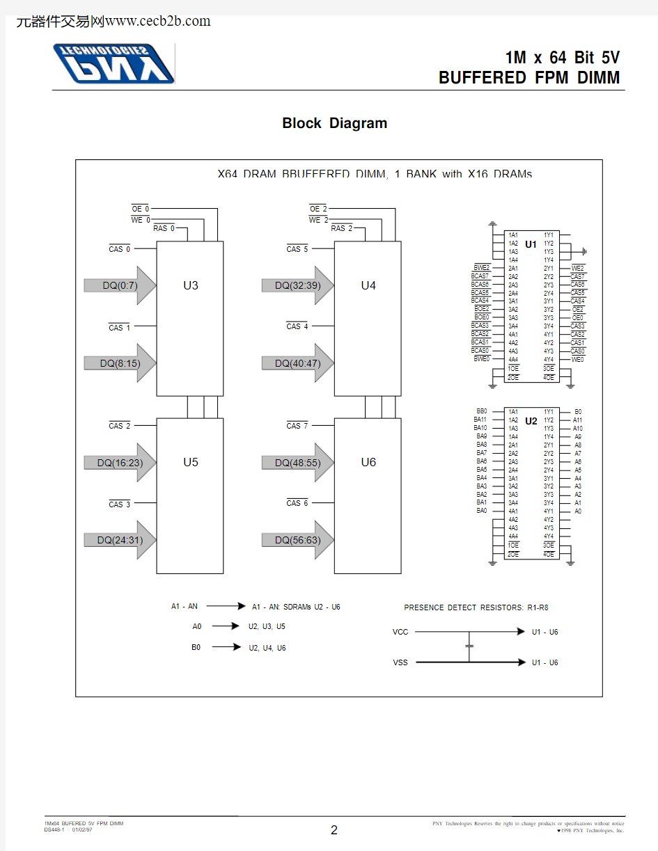
Block Diagram
Pin Descriptions
Pin Name Function
RAS#Row Address Strobe RAS# is used to strobe the row address.
CAS#Column Address Strobe CAS# is used to strobe the column address.
WE#Write Enable WE# is used to control read/write cycles.
OE#Output Enable OE# is the input/output control for the DQ lines.
A#, B0Address Lines Address lines are multiplexed to specify the row and column address. DQ0-DQ71Data Lines Data input/output lines.
Vdd Power Supply Power Supply 5V±0.5V
Vss Ground Ground
PD#, ID#Presence Detect Lines Presence detect lines used to indicate module type.
PDE Presence Detect Enable Enables buffers on PD lines.
NC No Connection Line is not connected in DIMM.
Presence Detect Matrix
DIMM Type PD1PD2PD3PD4PD5PD6PD7PD8ID0ID1 642035-D52G10JB Vss NC NC Vss Vss Vss Vss NC Vss Vss
642036-D52G10JB Vss NC NC Vss Vss NC NC NC Vss Vss
Absolute Maximum Ratings
Parameter Symbol Value Units
Voltage on any pin relative to Vss V in-1.0 to 7.0V
Short circuit output current I out50mA
Power dissipation Pt10W
Operating temperature T opr0 to +70°C
Storage temperature T st-55 to +125°C
NOTE: Permanent damage may occur if absolute maximum ratings are exceeded.
Device should be operated within recommended operating conditions only.
DC Characteristics (T A = 0 to 70C, Vcc = 5V ± 0.5V)
Parameter Symbol Min Typ Max Units Note Supply voltage Vss000V
Supply voltage Vcc 4.5 5.0 5.5V16 Input high voltage Vih 2.4-Vcc+0.5V16 Input low voltage Vil-0.5-0.8V16 Output high voltage Voh 2.4--V
Output low voltage Vol--0.8V
DC Current Consumption (T A = 0 to 70C, Vcc = 5V ± 0.5V)
Parameter Symbol Test Condition-50-60Unit Note Standby Current (TTL)I CC1(RAS# = CAS# = V IH)88mA17 Standby Current (CMOS)I CC2All inputs = Vcc - 0.2V44mA17 Operating Current Random Read/Write I CC3RAS#, CAS#, address cycling. t RC = t RC[MIN]624504mA17, 18 Operating Current Fast Page Mode I CC4RAS# = V IL, CAS#, Address cycling. t PC = t PC[MIN]264192mA17, 18 Operating Current EDO Page Mode I CC5RAS# = V IL, CAS#, Address cycling. t PC = t PC[MIN]N/A N/A mA17, 18 Refresh Current: RAS#-Only I CC6RAS# cycling, CAS#=V IH; t RC = t RC[MIN]624504mA17 Refresh Current: CAS# before RAS#I CC7RAS#, CAS#, address cycling t RC = t RC[MIN]624504mA17
Capacitance (T A = 0 to 70C, Vcc = 5V ± 0.5V, Vss = 0V)
Parameter Symbol Typ Max Units Note
Input capacitance (Address)C I1-5pF
Input capacitance (WE#, OE#)C I2-5pF
Input/Output capacitance (Data)C I/O-7pF
Input capacitance (CAS#)C I3-5pF
Input capacitance (RAS#)C14-10pF
AC Characteristics (T A = 0 to 70C, Vcc = 5V ± 0.5V, Vss = 0V)
Units Note
-50-60
Parameter Symbol
Min Max Min Max
Access time from column address t AA2530ns3, 5, 14 Column address setup to CAS# precharge t ACH1215ns
Column address hold time (from RAS#)t AR4050ns
Column address setup time t ASC00ns
Row address setup time t ASR00ns
Access time from CAS#t CAC1517ns3, 4, 14 Column address hold time t CAH810ns
CAS# pulse width t CAS810 0001010 000ns
CAS# to output in Low-Z t CLZ33ns
Data output hold after CAS# LOW t COH33ns
CAS# precharge time t CP810ns
Access time from CAS# precharge t CPA2835ns
CAS# to RAS# precharge time t CRP55ns
CAS# hold time t CSH4050ns
WRITE command to CAS# lead time t CWL810ns
Data-in hold time t DH810ns11 Data-in setup time t DS00ns11 Output buffer turn-off delay t OFF012015ns
EDO Page-mode read or write cycle time t PC2025ns
Access time from RAS#t RAC5060ns2, 3 RAS# to column address delay time t RAD15251530ns9 Row-address hold time t RAH1010ns
RAS# pulse width t RAS, t RASP5010 0006010 000ns
Random read/write cycle time t RC84104ns
RAS# to CAS# delay time t RCD20352043ns8 Read command hold time t RCH00ns
Read command setup time t RCS00ns
Refresh Period (1024 cycles)t REF1616ms15 RAS# precharge time t RP3040ns
RAS# to CAS# precharge time t RPC55ns
READ command hold time t RRH00ns
RAS# hold time t RSH1317ns
WRITE command to RAS# lead time t RWL1315ns
Transition Time tτ250250ns7
AC Characteristics (T A = 0 to 70C, Vcc = 5V ± 0.5V, Vss = 0V)
Parameter Symbol
-50-60
Units Note
Min Max Min Max
WRITE command hold time t WCH810ns
WRITE command hold time (RAS# referenced)t WCR3845ns
WE# command setup time t WCS00ns10 Output disable delay from WE#t WHZ012015ns
Write command pulse width t WP55ns
Notes
1.AC measurements assume t T = 5ns
2.Assumes that t RCD≤ t RCD (max.) and t RAD≥ t RAD (max.). If t RCD or t RAD is greater that the maximum recommended value shown in this table, t RAC
exceeds the value shown.
3.Measured with a load circuit equivilaent to 1 TTL load and 100pF.
4.Assumes that t RCD≥ t RCD (max.), t RAD≤ t RAD (max.).
5.Assumes that t RCD≤ t RCD (max.), t RAD≥ t RAD (max.).
6.t OFF (max.) defines the time at which the output achieves the open circuit condition and is not referenced to output voltage levels.
7.Vih (min.) and Vil (max.) are reference levels for measuring timing of input signals. Also, transition times are measured between Vih and Vil.
8.Operation with the t RCD (max.) limit insures that t RAC (max.) can be met, t RCD (max.) is specified as a reference point only, if t RCD is greater that the
specified t RCD (max.) limit, then the access time is controlled exclusively by t CAC.
9.Operation with the t RAD (max.) limit insures that t RAC (max.) can be met, t RAD (max.) is specified as a reference point only, if t RAD is greater that the
specified t RAD (max.) limit, then access time is controlled exclusively by t AA.
10.Early write cycle only (t WCS≥ t WCS (min.))
11.These parameters are referenced to CAS* leading edge in an early write cycle.
12.An initial pause of 100us is required after power up followed by a minimum of eight initialization cycles (any combination of cycles containing RAS*
clock such as RAS* only refresh)
13.t RASC defines RAS* pulse width in fast page mode cycles.
14.Access time is determined by the longer of t AA or t CAC or t ACP
15.t REF defined is 1024 refresh cycle.
16.All voltages referenced to Vss
17.Typical maximum current consumption levels
18.Column address changed once per cycle
t
RP
t RAS
t RC t CRP
t RCD
t CAS
t RSH
t CSH t RRH
t ASR
t RAH
t RAD
t ACH
t CAH t ASC
t AR
t RCS
t RCH
t CLZ
t CAC t RAC t AA t OFF
ADDR
WE
DQ CAS
RAS
ROW
COLUMN
ROW
VALID DATA
OPEN
OPEN
READ CYCLE
DON'T CARE
UNDEFINED
t RP
t RAS
t RC t CRP
t RCD
t CAS
t RSH t CSH
t ASR
t RAH
t RAD
t ACH
t CAH t ASC t AR t WP
t WCH t WCR t RWL
ADDR
DQ CAS
ROW
COLUMN
ROW
VALID DATA
EARLY WRITE CYCLE
DON'T CARE UNDEFINED
t WCS
t CWL t DH
t DS
t
RP
t
RASP
t
CRP
t
RCD
t
CSH
t
CAS
t
CP
t
CAS
t
PC
t
CP
t
CAS
t
RSH
t
CP
t
ASR
t
RAH
t
RAD
t
AR
t
ASC
t
CAH
t
ASC
t
CAH
t
ASC
t
CAH
t
RCS
t
RCH
t
OFF
t
CLZ
t
CAC
t
CPA
t
AA
t
COH
t
CAC
t
CPA
t
AA
t
CLZ
t
CAC
t
RAC
t
AA
ADDR
WE
DQ
DON'T CARE
UNDEFINED ROW ROW
COLUMN
COLUMN COLUMN
VALID
DATA
VALID
DATA
VALID
DATA
EDO-PAGE-MODE READ CYCLE
t
ACH
t
CAH
t
CAH
t
RRH OPEN
OPEN
t
RP
t
RASP
t
CRP
t
RCD
t
CSH
t
CAS
t
CP
t
CAS
t
PC
t
CP
t
CAS
t
RSH
t
CP
t
ASR
t
RAH
t
RAD
t
AR
t
ASC
t
CAH
t
ASC
t
CAH
t
ASC
t
CAH
t
DH
t
DS
t
COH
t
CAC
t
CAC
t
RAC
ADDR
WE
DQ
CAS
RAS
DON'T CARE
UNDEFINED ROW ROW
COLUMN (B)
COLUMN (A)COLUMN (N)
VALID Dout VALID Dout VALID Din
EDO-PAGE-MODE READ-EARLY-WRITE CYCLE
t
ACH
t
RCH
t
AA
t
PC
t
WCS
t
WCH
t
RCS
t
WHZ
t
CPA
t
AA
OPEN
t
RP
t
RASP
t
CRP
t
RCD
t
CSH
t
CAS
t
CP
t
CAS
t
PC
t
CP
t
CAS
t
RSH
t
CP
t
ASR
t
RAH
t
RAD
t
AR
t
ASC
t
CAH
t
ASC
t
CAH
t
ASC
t
CAH
t
WP
t
WP
t
WP
t
DH
t
DS
t
DH
t
DS
t
CAC
t
WCR
ADDR
WE
DQ
CAS
RAS
DON'T CARE
UNDEFINED ROW ROW
COLUMN
COLUMN COLUMN
VALID DATA VALID DATA VALID DATA
FAST/EDO-PAGE-MODE EARLY-WRITE CYCLE
t
ACH
t
ACH
t
ACH
t
WCH
t
CWL
t
WCS
t
WCH
t
CWL
t
WCS
t
WCH
t
CWL
t
WCS
t
DS
t
RWL
t
CRP
t
RCD
t
CSH
t
CAS
t
CP
t
ASR
t
RAH
t
RAD
t
ASC
t
CAH
t
AR
t
ASC
ROW COLUMN COLUMN
t
RCS
t
RCH
t
WPZ
t
RCS
OPEN
t
CLZ
t
CAC
t
RAC
t
AA
t
WHZ
OPEN
t
CLZ
DON'T CARE
UNDEFINED
VALID DATA
EDO READ CYCLE
( with /WE-controlled disable )
ADDR
WE
DQ
CAS
RAS
t RP
t RAS
t RC
t
CRP
t RPC
t ASR
t RAH
ROW
ROW
OPEN
/RAS-ONLY REFRESH CYCLE
DON'T CARE UNDEFINED
ADDR
Q RAS
WE
CASL / CASH
t RP
t RAS
t CP
t CHR
OPEN
DON'T CARE UNDEFINED
t RP
t RAS
t RPC t CSR
t RPC
t CSR
t CHR
t WRP t WRH
t WRP t WRH
WE
DQ
CAS
RAS
CBR REFRESH CYCLE
( Addresses = DON'T CARE )