TDA7269A, 规格书,Datasheet 资料
1/9
TDA7269A
June 2003 s WIDE SUPPLY VOLTAGE RANGE UP TO +20V
s SPLIT SUPPLY
s
HHIGH OUTPUT POWER 14+14W @THD = 10%, R L = 8?, V S = ±16V s NO POP AT TURN-ON/OFF s MUTE (POP FREE)
s STAND-BY FEATURE (LOW I q )
s SHORT CIRCUIT PROTECTION TO GND s
THERMAL OVERLOAD PROTECTION
DESCRIPTION
The TDA7269A is class AB Dual Audio Power ampli-fier assembled in the Multiwatt package, specially de-signed for high quality sound application as Hi-Fi music centers and stereo TV sets.
14W+14W STEREO AMPLIFIER WITH MUTE & ST-BY
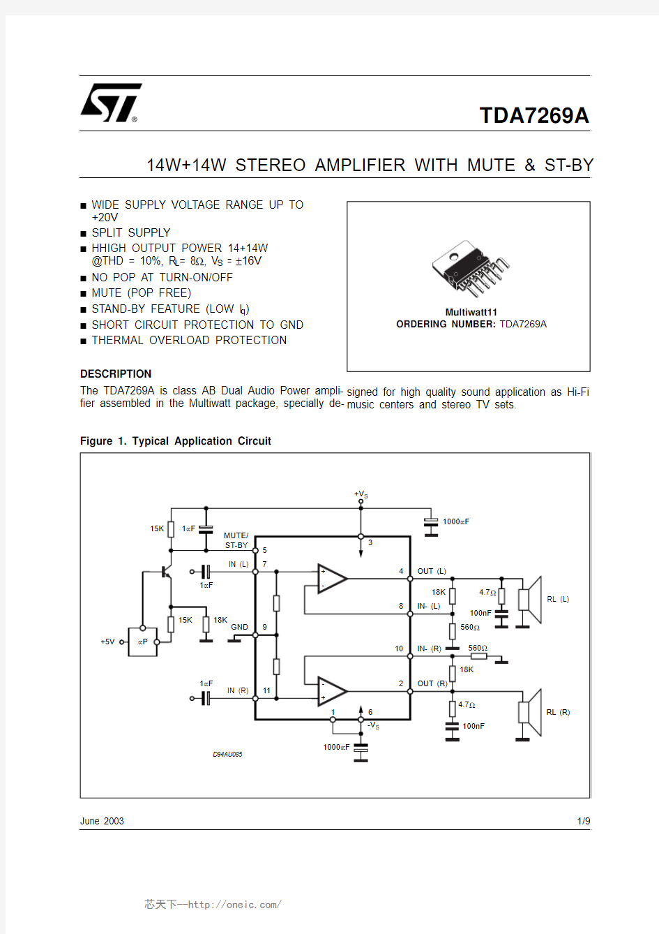
Figure 1. Typical Application Circuit
TDA7269A
ABSOLUTE MAXIMUM RATINGS
Symbol Parameter Value Unit V S DC Supply Voltage±22V
I O Output Power Current (internally limited)3A
P tot T otal Power Dissipation (Tamb = 70°C)40W T op Operating Temperature 0 to 70°C T stg, T j Storage and Junction T emperature-40 to 150°C
THERMAL DATA
Symbol Parameter Value Unit R th j-case Thermal Resistance Junction-case Max. 2.8°C/W
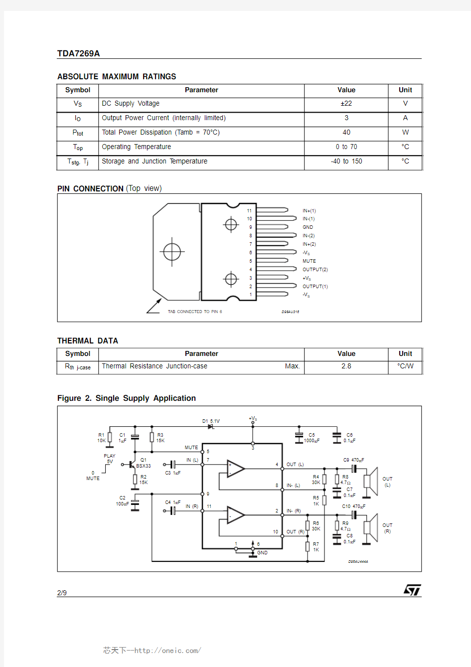
Figure 2. Single Supply Application
2/9
3/9
TDA7269A
ELECTRICAL CHARACTERISTCS (Refer to the test circuit V S = ±16V; R L = 8?; R S = 50?; G V = 30dB, f = 1KHz; T amb = 25°C, unless otherwise specified)
(*) In mute condition the current drawn from Pin 5 must be ≤650μA
Symbol Parameter
Test Condition
Min.Typ.
Max.Unit V S
Supply Voltage Range
R L = 8?±5±20V R L = 4?
±5
±15V I q Total Quiescent Current 60100mA V OS Input Offset Voltage
-25
25
mV I b Non Inverting Input Bias Current 500nA P O
Output Power
THD = 10%; R L = 8?;
V S = ±12.5V; R L = 4?; 1281410W W THD = 1%; R L = 8?;
V S = ±12.5V; R L = 4?;
96117.5W W THD
Total Harmonic Distortion
R L = 8?; P O = 1W; f = 1KHz; 0.03
%R L = 8?; P O = 0.1 to 7W; f = 100Hz to 15KHz; 0.7
%R L = 4?; P O = 1W; f = 1KHz; 0.02
%R L = 4?; V S = ±10V;P O = 0.1 to 5W; f = 100Hz to 15KHz;
1
%
C T Cross T alk f = 1KHz;f = 10KHz;
507060dB dB SR Slew Rate
6.5
10V/μs G OL Open Loop Voltage Gain 80dB e N Total Output Noise A Curve
f = 20Hz to 22KHz
348
μV μV R i Input Resistance 15
20K ?SVR Supply Voltage Rejection (each channel)
f = 100Hz; V R = 0.5V 60dB T j
Thermal Shut-down Junction Temperature
145
°C
MUTE FUNCTION [ref +V S ] (*)VT MUTE Mute /Play threshold -7-6-5
V A MUTE
Mute Attenuation
60
70
dB
STAND-BY FUNCTIONS [ref: +V S ] (only for Split Supply)VT ST -BY Stand-by Mute threshold -3.5
-2.5-1.5
V A ST -BY Stand-by Attenuation
110dB I qST -BY
Quiescent Current @ Stand-by
3
6mA
TDA7269A
MUTE STAND-BY FUNCTION
The pin 5 (MUTE/STAND-BY) controls the amplifier status by two different thresholds, referred to +V S.
–When V pin5 higher than = +V S -2.5V the amplifier is in Stand-by mode and the final stage generators are off.
–When V pin5 between +V S -2.5V and +V S -6V the final stage current generators are switched on and the amplifier is in mute mode.
–When V pin5 is lower than +V S -6V the amplifier is play mode.
Figure 3.
4/9
5/9
TDA7269A
Figure 4. Test and Application Circuit (Stereo Configuration)
APPLICATION SUGGESTIONS (Demo Board Schematic)
The recommended values of the external components are those shown the demoboard schematic different val-ues can be used, the following table can help the designer.
(*) Closed loop gain has to be ≥25dB
COMPONENT
SUGGESTION
VALUE
PURPOSE
LARGER THAN RECOMMENDED VALUE SMALLER THAN RECOMMENDED VALUE
R110K ?Mute Circuit Increase of Dz Biasing Current
R215K ?Mute Circuit V pin #5 Shifted Downward V pin #5 Shifted Upward R318K ?Mute Circuit V pin #5 Shifted Upward V pin #5 Shifted Downward R415K ?Mute Circuit V pin #5 Shifted Upward V pin #5 Shifted Downward R5, R818K ?Closed Loop Gain Setting (*)
Increase of Gain R6, R9560?Decrease of Gain R7, R10 4.7?Frequency Stability Danger of Oscillations
Danger of Oscillations C1, C21μF Input DC Decoupling Higher Low Frequency Cutoff C31μF St-By/Mute Time Constant
Larger On/Off Time Smaller On/Off Time C4, C61000μF Supply Voltage Bypass Danger of Oscillations C5, C70.1μF Supply Voltage Bypass Danger of Oscillations C8, C90.1μF Frequency Stability Dz
5.1V
Mute Circuit
TDA7269A
BRIDGE APPLICATION
Another application suggestion concerns the Bridge configuration , where the two power amplifiers are connected as shown by the schematic diagrams of figure 5 “Split Power Supply” , and figure 6 “Single Power Supply”.
This application shows,however, some operative limits due to dissipation and current capability of the out-put stage.
For this reason we recommend to use the TDA7269A in BTL with the following supply voltages depending on the used load impedance (for the single supply consider double Vs) :
±Vs (V) Rload (ohm)
148
11 6
104
The detected characteristics of THD vs Pout are shown in figg: 7, 8 and 9 for the different load impedances. With Rload = 8ohm , Vs = ±14V the maximum output power obtainable is 30W at THD = 10% (fig. 9). With Rload = 6ohm , Vs = ±12V the maximum output power obtainable is 28W at THD = 10% (fig. 8). With Rload = 4ohm , Vs = ±10V the maximum output power obtainable is 20W at THD=10% (fig. 7).
We suggest not to exceed the suggested supply voltages in order to avoid the current limiter intervention. Figure 5. Split Power Supply Application Diagram
6/9
TDA7269A Figure 6. Single Power Supply Application Diagram
Figure 7. Distortion vs Output Power
Figure 8. Distortion vs Output Power
Figure 9. Distortion vs Output Power
7/9
TDA7269A
8/9
TDA7269A Information furnished is believed to be accurate and reliable. However, STMicroelectronics assumes no responsibility for the consequences of use of such information nor for any infringement of patents or other rights of third parties which may result from its use. No license is granted
by implication or otherwise under any patent or patent rights of STMicroelectronics. Specifications mentioned in this publication are subject to change without notice. This publication supersedes and replaces all information previously supplied. STMicroelectronics products are not
authorized for use as critical components in life support devices or systems without express written approval of STMicroelectronics.
The ST logo is a registered trademark of STMicroelectronics
?2002 STMicroelectronics - All Rights Reserved
Australia - Brazil - Canada - China - Finland - France - Germany - Hong Kong - India - Israel - Italy - Japan -Malaysia - Malta - Morocco - Singapore - Spain - Sweden - Switzerland - United Kingdom - United States.
https://www.360docs.net/doc/e1372505.html,
9/9
道岔转辙部位框架尺寸表
43kg、50kg普通(AT型)1/9道岔转辙部分各部尺寸表
车站名: 道岔编号: 调查日期: 调查人: 43kg、50kg普通(AT型)1/12道岔转辙部分各部尺寸表
道岔查照间隔整修方案参考表
从此表可知:1、叉心轨轨距必须控制在1433?1438之间,最好是1436mm 2 、轮缘槽宽度较小时,轨距也要相应减小,最低轨距为-2mm护轨槽宽不能超过42mm翼轨槽宽不能超过45mm 3 、槽宽过大时,轨距也要相应增大。最大为+3mm护轨槽宽为44mm翼轨槽宽46?48mm
爱人者,人恒爱之;敬人者,人恒敬之;宽以济猛,猛以济宽,政是以和。将军额上能跑马,宰相肚里能撑船。 最高贵的复仇是宽容。有时宽容引起的道德震动比惩罚更强烈。 君子贤而能容罢,知而能容愚,博而能容浅,粹而能容杂。 宽容就是忘却,人人都有痛苦,都有伤疤,动辄去揭,便添新创,旧痕新伤难愈合,忘记昨日的是非,忘记别人先前对自己的指责和谩骂,时间是良好的止痛剂,学会忘却,生活才有阳光,才有欢乐。 不要轻易放弃感情,谁都会心疼;不要冲动下做决定,会后悔一生。也许只一句分手,就再也不见;也许只一次主动,就能挽回遗憾。 世界上没有不争吵的感情,只有不肯包容的心灵;生活中没有不会生气的人,只有不知原谅的心。 感情不是游戏,谁也伤不起;人心不是钢铁,谁也疼不起。好缘分,凭的就是真心真意;真感情,要的就是不离不弃。
这世上,别指望人人都对你好,对你好的人一辈子也不会遇到几个。人心只有一颗,能放在心上的人毕竟不多;感情就那么一块,心里一直装着你其实是难得。 动了真情,情才会最难割;付出真心,心才会最难舍。 你在谁面前最蠢,就是最爱谁。其实恋爱就这么简单,会让你智商下降,完全变了性格,越来越不果断。 所以啊,不管你有多聪明,多有手段,多富有攻击性,真的爱上人时,就一点也用不上。 这件事情告诉我们。谁在你面前很聪明,很有手段,谁就真的不爱你呀。 遇到你之前,我以为爱是惊天动地,爱是轰轰烈烈抵死缠绵;我以为爱是荡气回肠,爱是热血沸腾幸福满满。 我以为爱是窒息疯狂,爱是炙热的火炭。婚姻生活牵手走过酸甜苦辣温馨与艰难,我开始懂得爱是经得起平淡。 爱人者,人恒爱之;敬人者,人恒敬之;宽以济猛,猛以济宽,政是以和。将军额上能跑马,宰相肚里能撑船。 最高贵的复仇是宽容。有时宽容引起的道德震动比惩罚更强烈。
GLC(07)02-18#道岔各部框架尺寸(直通线)
GLC(07)02—18#道岔各部框架尺寸(直通线) 一、尖轨尖端绝对位置:距岔前轨端1951mm。距4#枕中心向前120mm。 二、转辙部分框架尺寸:(±1.0mm)(两基本轨作用边测量) 1、尖轨尖端:1435,mm。 2、第一牵引点中心:距尖轨尖端470mm。1437.5mm。 3、12#--13#枕间:距尖轨尖端5168mm。1461.8mm。 4、第二牵引点中心:距第一牵引点中心4800mm。1462.1mm。 5、第三牵引点中心:距第二牵引点中心5400mm。1504.2mm。 6、21#--22#枕间:距尖轨尖端10847mm。1506mm。 7、35#枕中心:直股181mm。曲股181.2mm。(弹性可弯中心) 8、39#枕向后110mm:直股231.6mm。曲股231.9mm。 9、尖轨长度:21450mm。基本轨长度:24592mm。 三|辙岔部分框架尺寸:(两翼轨作用边测量) 1、岔趾:436.2mm。81#枕:423.9mm。82#枕:398.2mm。83#枕:372.1mm。84#枕:345.7mm。 85#枕:319mm。86#枕:291.9mm。87#枕:264.5mm。88#枕:236.8mm。89#枕:208.8mm。 2、第一间隔铁中心:194.4。 3、第二间隔铁中心:165.9。 4、第三间隔铁中心:132.7。 5、心轨理论尖端:119mm。(距92#枕中心向后100mm)(第一牵引点中心距92#枕中心 350mm) 四、长短心轨支距 1、第二牵引点中心:132.1mm。 2、第一间隔铁中心:157.4mm。 3、第二间隔铁中心:179.6mm。 4、第三间隔铁中心:213.3mm。 5、第一顶铁(短心轨)中心:233.8mm。 6、第二顶铁(短心轨)中心:257mm。 7、第三顶铁(短心轨)中心:291.2mm。 8、岔跟尖轨尖端:315mm。 9、最后间隔铁中心:567.8mm。 五、导曲线支距 尖跟垂直于基本轨位置向后2000mm开始向后每2000mm一点,共计15个点,支距如下:273.5mm、318.9mm、367.9mm、420.6mm、477mm、536.9mm、600.6mm、667.8mm、738.7mm、813.2mm、891.4mm、973.2mm、1058.7mm、1147.8mm、1240.5mm。