BT134-F中文资料
Absolute Maximum Ratings ( T J = 25°C unless otherwise specified )
Symbol
Parameter
Condition Ratings
Units
V DRM Repetitive Peak Off-State Voltage 600
V I T(RMS)R.M.S On-State Current T C = 104 °C
4A I TSM Surge On-State Current One Cycle, 50Hz/60Hz, Peak, Non-Repetitive 25/27A I 2t I 2t
t = 10ms
3.1A 2s P GM Peak Gate Power Dissipation 5
W P G(AV)Average Gate Power Dissipation Over any 20ms period 0.5W I GM Peak Gate Current 2A V GM Peak Gate Voltage
5V T J Operating Junction Temperature - 40 ~ 125°C T STG
Storage Temperature
- 40 ~ 150
°C
BT134-F
Nov, 2003. Rev. 0
Features
◆ Repetitive Peak Off-State Voltage : 600V ◆ R.M.S On-State Current ( I T(RMS)= 4 A )◆ High Commutation dv/dt
General Description
This device is suitable for low power AC switching applica-tion, phase control application such as fan speed and tem-perature modulation control, lighting control and static
switching relay.
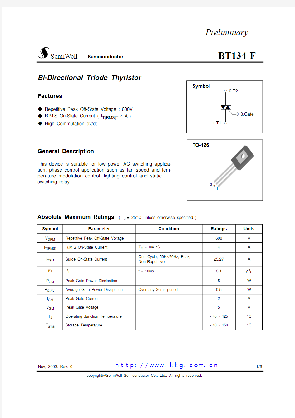
2.T2
3.Gate
1.T1
Symbol
○
○
○
▼▲
1/6
SemiWell Semiconductor Bi-Directional Triode Thyristor
copyright@SemiWell Semiconductor Co., Ltd., All rights reserved.
TO-126
3
2
1
Preliminary
http://www.kkg.com.cn
Electrical Characteristics
Symbol Items Conditions
Ratings
Unit Min.Typ.
Max.
I DRM Repetitive Peak Off-State
Current
V D = V DRM, Single Phase, Half Wave
T J = 125 °C──
0.5mA
V TM Peak On-State Voltage I T = 5 A, Inst. Measurement── 1.7V
I+GT1Ⅰ
Gate Trigger Current V D = 6 V, R L=10Ω──25
mA
I -GT1Ⅱ──25 I -GT3Ⅲ──25 I+GT3Ⅳ──70
V+GT1Ⅰ
Gate Trigger Voltage V D = 6 V, R L=10Ω── 1.5
V
V-GT1Ⅱ── 1.5
V-GT3Ⅲ── 1.5
V+GT3Ⅳ── 2.5
V GD Non-Trigger Gate Voltage T J = 125 °C, V D = 1/2 V DRM0.2──V
(dv/dt)c Critical Rate of Rise Off-State
Voltage at Commutation
T J = 125 °C, [di/dt]c = -0.75 A/ms,
V D=2/3 V DRM
5.0──V/?
I H Holding Current─5─mA
R th(j-c)Thermal Impedance Junction to case── 3.5°C/W BT134-F
2/6http://www.kkg.com.cn
BT134-F
Fig 3. On State Current vs.Fig 4. On State Current vs.
( Non-Repetitive ) Junction Temperature
4/6
BT134-F
Fig 8. Transient Thermal Impedance
Fig 7. Gate Trigger Current vs. Junction Temperature
Fig 9. Gate Trigger Characteristics Test Circuit
G
G
G
Test Procedure ⅠTest Procedure ⅡTest Procedure Ⅲ10?
G
Test Procedure Ⅳ
http://www.kkg.com.cn
Dim.
mm Inch Min.Typ.
Max.Min.Typ.Max.
A7.57.90.2950.311
B10.811.20.4250.441
C14.214.70.5590.579
D 2.7 2.90.1060.114
E 3.80.150
F 2.50.098
G 1.2 1.50.0470.059
H 2.30.091
I 4.60.181
J0.480.620.0190.024
K0.70.860.0280.034
L 1.40.055
φ 3.20.126
5/6
BT134-F TO-126 Package Dimension
http://www.kkg.com.cn
Dim.mm
Inch Min.Typ.
Max.Min.Typ.
Max.A 7.57.90.2950.311B 10.811.20.4250.441C 14.214.70.5590.579D 2.7
2.9
0.106
0.114
E 3.80.150
F 2.5
0.098
G 1.2
1.5
0.047
0.059
H 2.30.091I 4.6
0.181
J 0.480.620.0190.024K 0.7
0.86
0.028
0.034
L 1.40.055M
5.00.197φ
3.2
0.126
BT134-F
TO-126 Package Dimension, Forming
6/6
http://www.kkg.com.cn