4N35 datasheet 通
4N35/ 4N36/ 4N37/ 4N38
Document Number 83717Rev. 1.5, 27-Jan-05
Vishay Semiconductors
https://www.360docs.net/doc/e48338737.html,
1
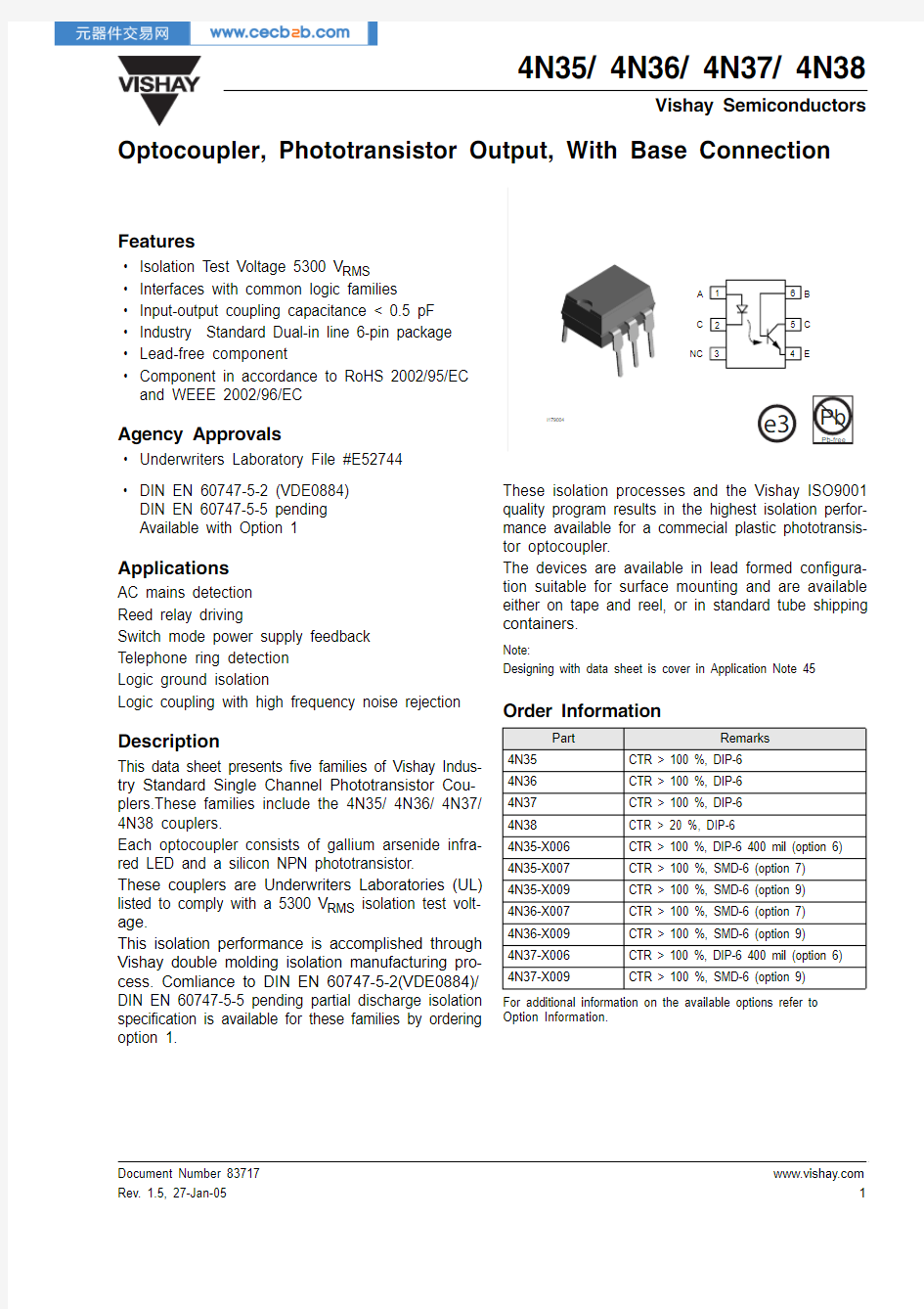
Optocoupler, Phototransistor Output, With Base Connection
Features
?Isolation Test Voltage 5300 V RMS
?Interfaces with common logic families
?Input-output coupling capacitance < 0.5 pF ?Industry Standard Dual-in line 6-pin package ?Lead-free component
?
Component in accordance to RoHS 2002/95/EC and WEEE 2002/96/EC
Agency Approvals
?Underwriters Laboratory File #E52744 ?DIN EN 60747-5-2 (VDE0884)DIN EN 60747-5-5 pending Available with Option 1
Applications
AC mains detection Reed relay driving
Switch mode power supply feedback Telephone ring detection Logic ground isolation
Logic coupling with high frequency noise rejection
Description
This data sheet presents five families of Vishay Indus-try Standard Single Channel Phototransistor Cou-plers.These families include the 4N35/ 4N36/ 4N37/4N38 couplers.
Each optocoupler consists of gallium arsenide infra-red LED and a silicon NPN phototransistor.
These couplers are Underwriters Laboratories (UL)listed to comply with a 5300 V RMS isolation test volt-age.
This isolation performance is accomplished through Vishay double molding isolation manufacturing pro-cess. Comliance to DIN EN 60747-5-2(VDE0884)/DIN EN 60747-5-5 pending partial discharge isolation specification is available for these families by ordering option 1.
These isolation processes and the Vishay ISO9001quality program results in the highest isolation perfor-mance available for a commecial plastic phototransis-tor optocoupler.
The devices are available in lead formed configura-tion suitable for surface mounting and are available either on tape and reel, or in standard tube shipping containers.
Note:
Designing with data sheet is cover in Application Note 45
Order Information
For additional information on the available options refer to Option Information.
Part
Remarks
4N35CTR > 100 %, DIP-64N36CTR > 100 %, DIP-64N37CTR > 100 %, DIP-64N38CTR > 20 %, DIP-6
4N35-X006CTR > 100 %, DIP-6 400 mil (option 6)4N35-X007CTR > 100 %, SMD-6 (option 7)4N35-X009CTR > 100 %, SMD-6 (option 9)4N36-X007CTR > 100 %, SMD-6 (option 7)4N36-X009CTR > 100 %, SMD-6 (option 9)4N37-X006CTR > 100 %, DIP-6 400 mil (option 6)4N37-X009
CTR > 100 %, SMD-6 (option 9)
https://www.360docs.net/doc/e48338737.html, 2
Document Number 83717
Rev. 1.5, 27-Jan-05
4N35/ 4N36/ 4N37/ 4N38
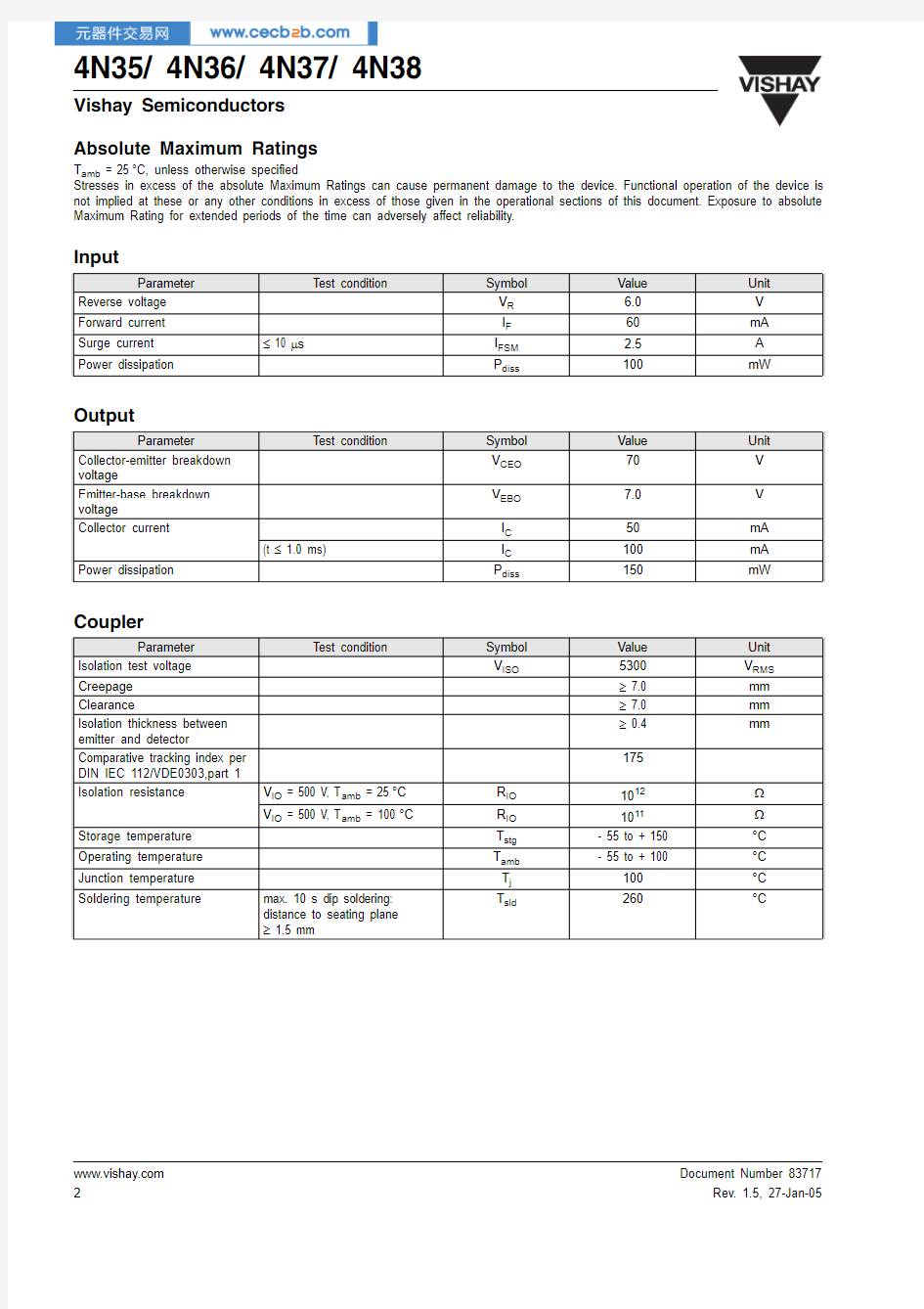
Vishay Semiconductors Absolute Maximum Ratings
T amb = 25°C, unless otherwise specified
Stresses in excess of the absolute Maximum Ratings can cause permanent damage to the device. Functional operation of the device is not implied at these or any other conditions in excess of those given in the operational sections of this document. Exposure to absolute Maximum Rating for extended periods of the time can adversely affect reliability.
Input
Output
Coupler
Parameter
Test condition
Symbol Value Unit Reverse voltage V R 6.0V Forward current I F 60mA Surge current ≤ 10 μs
I FSM 2.5A Power dissipation
P diss
100
mW
Parameter
Test condition
Symbol Value Unit Collector-emitter breakdown voltage
V CEO 70V Emitter-base breakdown voltage
V EBO 7.0V Collector current
I C 50mA (t ≤ 1.0 ms)
I C 100mA Power dissipation
P diss
150
mW
Parameter
Test condition
Symbol Value Unit Isolation test voltage V ISO
5300V RMS Creepage ≥ 7.0mm Clearance
≥ 7.0mm Isolation thickness between emitter and detector
≥ 0.4mm
Comparative tracking index per DIN IEC 112/VDE0303,part 1175Isolation resistance V IO = 500 V, T amb = 25°C R IO 1012?V IO = 500 V, T amb = 100°C
R IO 1011?Storage temperature T stg - 55 to + 150°C Operating temperature T amb - 55 to + 100
°C Junction temperature T j 100°C Soldering temperature
max. 10 s dip soldering: distance to seating plane ≥ 1.5 mm
T sld
260
°C
4N35/ 4N36/ 4N37/ 4N38
Document Number 83717Rev. 1.5, 27-Jan-05
Vishay Semiconductors
https://www.360docs.net/doc/e48338737.html,
3
Electrical Characteristics
T amb = 25°C, unless otherwise specified
Minimum and maximum values are testing requirements. Typical values are characteristics of the device and are the result of engineering evaluation. Typical values are for information only and are not part of the testing requirements.
Input
1) Indicates JEDEC registered value
Output
1)
Indicates JEDEC registered value
Coupler
1)
Indicates JEDEC registered value
Parameter
T est condition
Symbol Min
T yp.Max Unit Forward voltage 1)I F = 10 mA
V F 1.3 1.5V I F = 10 mA, T amb = - 55°C V F 0.9 1.3 1.7V Reverse current 1)V R = 6.0 V I R 0.110
μA Capacitance
V R = 0, f = 1.0 MHz
C O
25
pF
Parameter
T est condition
Part Symbol Min Typ.Max Unit Collector-emitter breakdown voltage 1)
I C = 1.0 mA
4N35
BV CEO 30V 4N36BV CEO 30V 4N37BV CEO 30V 4N38
BV CEO 80V Emitter-collector breakdown voltage 1)
I E = 100 μA
BV ECO
7.0V Collector-base breakdown voltage
1)
I C = 100 μA, I B = 1.0 μA
4N35BV CBO 70V 4N36BV CBO 70V 4N37BV CBO 70V 4N38
BV CBO 80
V
Collector-emitter leakage current
1)
V CE = 10 V, I F = 0
4N35I CEO 5.050nA 4N36
I CEO 5.050nA V CE = 10 V, I F =04N37I CEO 5.0
50nA V CE = 60 V, I F = 04N38I CEO 50nA V CE = 30 V, I F = 0, T amb = 100°C
4N35I CEO 500μA 4N36I CEO 500μA 4N37
I CEO 500
μA V CE = 60 V, I F = 0, T amb = 100°C
4N38I CEO 6.0μA Collector-emitter capacitance
V CE = 0
C CE
6.0
pF
Parameter
T est condition
Symbol Min T yp.Max Unit Resistance, input to output 1)V IO = 500 V R IO 1011
?Capacitance (input-output)
f = 1.0 MHz
C IO
0.5
pF
https://www.360docs.net/doc/e48338737.html, 4
Document Number 83717
Rev. 1.5, 27-Jan-05
4N35/ 4N36/ 4N37/ 4N38
Vishay Semiconductors Current Transfer Ratio
1)
Indicates JEDEC registered value
Switching Characteristics
1) Indicates JEDEC registered value
Typical Characteristics (Tamb = 25 °C unless otherwise specified)
Parameter
Test condition
Part Symbol Min T yp.Max Unit DC Current Transfer Ratio 1)
V CE = 10 V , I F = 10 mA
4N35CTR DC 100%4N36CTR DC 100%4N37
CTR DC 100%V CE = 10 V , I F = 20 mA 4N38CTR DC 20%
V CE = 10 V , I F = 10 mA, T A = - 55 to + 100°C
4N35CTR DC 4050%4N36CTR DC 4050%4N37CTR DC 40
50%4N38
CTR DC
30
%
Parameter Test condition
Symbol Min Typ.Max Unit Switching time 1)
I C = 2 mA, R L = 100 ?, V CC = 10 V
t on , t off
10
μs
Figure 1. Forward Voltage vs. Forward Current
i4n25_01
100
101.1
0.7
0.80.91.01.11.2
1.3
1.4I F -Forward Current -mA
V F -F o r w a r d V o l t a g e -V
Figure 2. Normalized Non-Saturated and Saturated CTR vs. LED
Current
i4n25_02
0.0
0.5
1.0
1.5
110100
I F -LED Current -mA
N C T R -N o r m l i z e d C T R
4N35/ 4N36/ 4N37/ 4N38
Document Number 83717Rev. 1.5, 27-Jan-05
Vishay Semiconductors
https://www.360docs.net/doc/e48338737.html,
5
Figure 3. Normalized Non-saturated and Saturated CTR vs. LED
Current Figure 4. Normalized Non-saturated and saturated CTR vs. LED
Current
Figure 5. Normalized Non-saturated and saturated CTR vs. LED
Current
i4n25_03
0.0
0.5
1.0
1.5I F -LED Current -mA
N C T R -N o r m a l i z e d C T R
i4n25_04
0.0
0.5
1.0
1.5I F -LED Current -mA
N C T R -N o r m a l i z e d C T R
i4n25_05
0.0
0.5
1.0
1.5I F -LED Current -mA
N C T R -N o r m a l i z e d C T R
Figure 6. Collector-Emitter Current vs. Temperature and LED
Current
Figure 7. Collector-Emitter Leakage Current vs.Temp.
Figure 8. Normalized CTRcb vs. LED Current and Temp.
i4n25_06
6050
40
30
20
10
I F -LED Current -mA
I c e -C o l l e c t o r C u r r e n t -m A
i4n25_07
100
80
60
40
20
–20
1010
10
101010
1010–2
–10
12
3
45T A -Ambient Temperature -°C
I c e o -C o l l e c t o r -E m i t t e r -n A
Typical
V ce =10V i4n25_08
0.00.5
1.0
1.5
I F -LED Current -mA
N C T R c b -N o r m a l i z e d C T R c b
.1
1
10
100
https://www.360docs.net/doc/e48338737.html, 6
Document Number 83717
Rev. 1.5, 27-Jan-05
4N35/ 4N36/ 4N37/ 4N38
Vishay Semiconductors
Figure 9. Normalized Photocurrent vs. I F and Temp.
Figure 10. Normalized Non-saturated HFE vs. Base Current and
Temperature
Figure 11. Normalized HFE vs. Base Current and Temp.i4n25_09
0.
0.01
11
10
I F -LED Current -mA
N o r m a l i z e d P h o t o c u r r e n t
.1
110100
i4n25_10
0.4
0.6
1.0
1.2Ib -Base Current -μA
N H F E -N o r m a l i z e d H F E
0.8
i4n25_11
0.0
0.5
1.0
1.5
N H F E (s a t )-N o r m a l i z e d S a t u r a t e d H F E
1
10
100
1000
Ib -Base Current -μ
A
Figure 12. Propagation Delay vs. Collector Load Resistor
Figure 13. Switching Timing
Figure 14. Switching Schematic
i4n25_12
1000RL -Collector Load Resistor -k ?
t P L H -P r o p a
g a t i o n D e l a y -μs
.1
1
10
100
t P H L -P r o p a g a t i o n D e l a y -μs
i4n25_13
I F
V i4n25_14
V =5.0V
F=10V O
I F =10mA
4N35/ 4N36/ 4N37/ 4N38
Document Number 83717Rev. 1.5, 27-Jan-05
Vishay Semiconductors
https://www.360docs.net/doc/e48338737.html,
7
Package Dimensions in Inches (mm)
For 4N35/36/37/38..... see DIL300-6 Package dimension in the Package Section.
For products with an option designator (e.g. 4N35-X006 or 4N36-X007)..... see DIP-6 Package dimensions in the Package Section.
DIL300-6 Package Dimensions
https://www.360docs.net/doc/e48338737.html, 8Document Number 83717
Rev. 1.5, 27-Jan-05
4N35/ 4N36/ 4N37/ 4N38 Vishay Semiconductors
4N35/ 4N36/ 4N37/ 4N38
Document Number 83717Rev. 1.5, 27-Jan-05
Vishay Semiconductors
https://www.360docs.net/doc/e48338737.html,
9
Ozone Depleting Substances Policy Statement
It is the policy of Vishay Semiconductor GmbH to
1.Meet all present and future national and international statutory requirements.
2.Regularly and continuously improve the performance of our products, processes, distribution and
operatingsystems with respect to their impact on the health and safety of our employees and the public, as well as their impact on the environment.It is particular concern to control or eliminate releases of those substances into the atmosphere which are known as ozone depleting substances (ODSs).
The Montreal Protocol (1987) and its London Amendments (1990) intend to severely restrict the use of ODSs and forbid their use within the next ten years. Various national and international initiatives are pressing for an earlier ban on these substances.
Vishay Semiconductor GmbH has been able to use its policy of continuous improvements to eliminate the use of ODSs listed in the following documents.
1.Annex A, B and list of transitional substances of the Montreal Protocol and the London Amendments respectively
2.Class I and II ozone depleting substances in the Clean Air Act Amendments of 1990 by the Environmental Protection Agency (EPA) in the USA
3.Council Decision 88/540/EEC and 91/690/EEC Annex A, B and C (transitional substances) respectively.Vishay Semiconductor GmbH can certify that our semiconductors are not manufactured with ozone depleting substances and do not contain such substances.
We reserve the right to make changes to improve technical design
and may do so without further notice.
Parameters can vary in different applications. All operating parameters must be validated for each customer application by the customer. Should the buyer use Vishay Semiconductors products for any unintended or unauthorized application, the buyer shall indemnify Vishay Semiconductors against all claims, costs, damages, and expenses, arising out of, directly or indirectly, any claim of personal
damage, injury or death associated with such unintended or unauthorized use.
Vishay Semiconductor GmbH, P.O.B. 3535, D-74025 Heilbronn, Germany
Telephone: 49 (0)7131 67 2831, Fax number: 49 (0)7131 67 2423
Legal Disclaimer Notice
Vishay Document Number: https://www.360docs.net/doc/e48338737.html, Revision: 08-Apr-051
Notice
Specifications of the products displayed herein are subject to change without notice. Vishay Intertechnology, Inc., or anyone on its behalf, assumes no responsibility or liability for any errors or inaccuracies.
Information contained herein is intended to provide a product description only. No license, express or implied, by estoppel or otherwise, to any intellectual property rights is granted by this document. Except as provided in Vishay's terms and conditions of sale for such products, Vishay assumes no liability whatsoever, and disclaims any express or implied warranty, relating to sale and/or use of Vishay products including liability or warranties relating to fitness for a particular purpose, merchantability, or infringement of any patent, copyright, or other intellectual property right. The products shown herein are not designed for use in medical, life-saving, or life-sustaining applications. Customers using or selling these products for use in such applications do so at their own risk and agree to fully
indemnify Vishay for any damages resulting from such improper use or sale.