HLMP-CM16-VY0XX中文资料
Agilent T-13/4 (5 mm) Precision Optical Performance InGaN Blue and Green Lamps
Data Sheet
Features
?Well defined spatial radiation pattern ?Viewing angles: 15? and 30??High luminous output ?Colors: 472 nm Blue,526 nm Green
?Superior resistance to moisture ?UV resistant epoxy
Benefits
?Superior performance in outdoor environments ?Wavelengths suitable for color mixing in full color (RGB) signs Applications
?Commercial outdoor signs ?Automotive interior lights ?Front panel indicators ?Front panel backlighting
Description
These high intensity blue and green LEDs are based on InGaN material technology. InGaN is the most efficient and cost effective material for LEDs in the blue and green region of the spectrum.The 472 nm typical dominant wavelength for blue and 526 nm typical dominant wavelength for green are well suited to color mixing in full color signs.These LED lamps are untinted,nondiffused, T-13/4 packages incorporating second generation optics producing well defined spatial radiation patterns at specific viewing cone angles.
CAUTION: HLMP-CBxx and HLMP-CMxx LEDs are Class 1 ESD sensitive. Please observe appropriate precautions during handling and processing. Refer to Agilent Application Note AN-1142 for additional details.
These lamps are made with an advanced optical grade epoxy,offering superior high
temperature and high moisture resistance performance in outdoor signal and sign
applications. The high maximum LED junction temperature limit of +130?C enables high
temperature operation in bright sunlight conditions. The package epoxy contains both UV-A and UV-B inhibitors to reduce the effects of long term exposure to direct sunlight.
These lamps are available in two viewing angle options to give the designer flexibility with optical design.
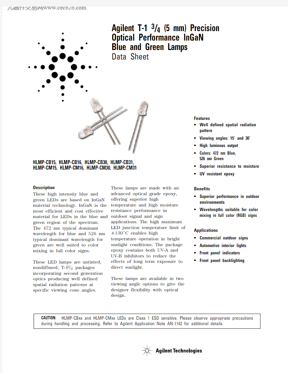
HLMP-CB15, HLMP-CB16, HLMP-CB30, HLMP-CB31,HLMP-CM15, HLMP-CM16, HLMP-CM30, HLMP-CM31
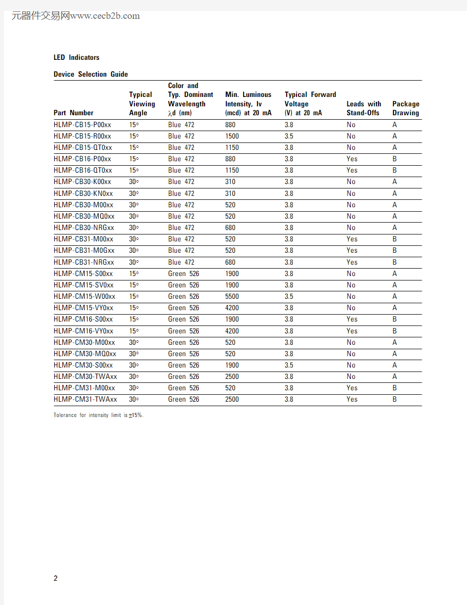
LED Indicators
Device Selection Guide
Color and
Typical Typ. Dominant Min. Luminous Typical Forward
Viewing Wavelength Intensity, Iv Voltage Leads with Package Part Number Angleλd (nm)(mcd) at 20 mA(V) at 20 mA Stand-Offs Drawing HLMP-CB15-P00xx15°Blue 472880 3.8No A HLMP-CB15-R00xx15°Blue 4721500 3.5No A HLMP-CB15-QT0xx15°Blue 4721150 3.8No A HLMP-CB16-P00xx15°Blue 472880 3.8Yes B HLMP-CB16-QT0xx15°Blue 4721150 3.8Yes B HLMP-CB30-K00xx30°Blue 472310 3.8No A HLMP-CB30-KN0xx30°Blue 472310 3.8No A HLMP-CB30-M00xx30°Blue 472520 3.8No A HLMP-CB30-MQ0xx30°Blue 472520 3.8No A HLMP-CB30-NRGxx30°Blue 472680 3.8No A HLMP-CB31-M00xx30°Blue 472520 3.8Yes B HLMP-CB31-M0Gxx30°Blue 472520 3.8Yes B HLMP-CB31-NRGxx30°Blue 472680 3.8Yes B HLMP-CM15-S00xx15°Green 5261900 3.8No A HLMP-CM15-SV0xx15°Green 5261900 3.8No A HLMP-CM15-W00xx15°Green 5265500 3.5No A HLMP-CM15-VY0xx15°Green 5264200 3.8No A HLMP-CM16-S00xx15°Green 5261900 3.8Yes B HLMP-CM16-VY0xx15°Green 5264200 3.8Yes B HLMP-CM30-M00xx30°Green 526520 3.8No A HLMP-CM30-MQ0xx30°Green 526520 3.8No A HLMP-CM30-S00xx30°Green 5261900 3.5No A HLMP-CM30-TWAxx30°Green 5262500 3.8No A HLMP-CM31-M00xx30°Green 526520 3.8Yes B HLMP-CM31-TWAxx30°Green 5262500 3.8Yes B
Tolerance for intensity limit is ±15%.
Part Numbering System
HLMP - X X XX - X X X XX
Mechanical Options
00: Bulk
DD: Ammo Pack
YY: Flexi bin, Bulk
ZZ: Flexi bin, Ammo Pack
Color Bin Selection
0: Full color range
A: Color bin 1 & 2 only
G: Color bin 2, 3 & 4 only
Maximum Intensity Bin
0: No maximum Iv bin limit
Others: Refer to Intensity Bin Limit Table
Minimum Intensity Bin
Refer to Device Selection Guide
Viewing Angle and Standoff Options
15: 15 degree without standoff
16: 15 degree with standoff
30: 30 degree without standoff
31: 30 degree with standoff
Color
B: Blue
M: Green
Package
C: T-1 3/4 (5 mm) round lamp
Notes:
1. Dimensions in mm.
2. Tolerance ±0.1 mm unless otherwise noted.
5.80 ± 0.20 (0.039)
HLMP-Cx15 and HLMP-Cx30
Package Dimensions
5.80 ± 0.20 (0.039)
HLMP-Cx16 and HLMP-Cx31
HLMP-Cx16HLMP-Cx31d = 12.60 ± 0.25 (0.496 ± 0.010) d = 12.22 ± 0.50 (0.481 ± 0.020)
Absolute Maximum Ratings at T A = 25?C
Parameter Blue and Green
DC Forward Current[1]30 mA
Peak Pulsed Forward Current100 mA
Average Forward Current30 mA
Reverse Voltage (I R = 100 μA) 5 V
Power Dissipation120 mW
LED Junction Temperature130?C
Operating Temperature Range–40?C to +80?C
Storage Temperature Range–40?C to +100?C
Soldering Temperature260?C for 5 seconds
Note:
1.Derate linearly as shown in Figure 5 for temperatures above 50?C.
Electrical/Optical Characteristics at T A = 25?C
Parameter Symbol Min.Typ.Max.Units Test Conditions Forward Voltage V F 3.5 4.0V I F = 20 mA
Reverse Voltage V R5I R = 100 μA
Peak Wavelength Peak of Wavelength of Blue (λd = 472 nm)λpeak470nm Spectral Distribution Green (λd = 526 nm)524at I F = 20 mA Spectral Halfwidth Wavelength Width Blue (λd = 472 nm)?λ1/235nm at Spectral Power Green (λd = 526 nm)47Point at I F = 20 mA Capacitance C43pF V F = 0, F = 1 MHz Luminous Efficacy Emitted Luminous Blue (λd = 472 nm)ηv75lm/W Power/Emitted Radiant Green (λd = 526 nm)520Power
Thermal Resistance RΘJ-PIN240?C/W LED Junction-to-
Cathode Lead
Figure 1. Relative intensity vs. wavelength.
Figure 2. Forward current vs. forward voltage for devices with 3.5 V typical Vf.Figure 4. Relative luminous intensity vs.forward current.WAVELENGTH – nm
R E L A T I V E I N T E N S I T Y
1.0 0.9 0.8 0.7 0.6 0.5 0.4 0.3 0.2 0.1
00
30
2515102.0 3.25
20 2.82.4 3.6F O R W A R D C U R R E N T
FORWARD VOLTAGE
2.62.2
3.0 3.4 3.8
1.5
0.5
I N T E N S I T Y N O R M A L I Z E D A T 20 m A
I F – FORWARD CURRENT – mA 051530
1.0
102520Figure 5. Maximum forward current vs.ambient temperature.
Figure 6. Spatial radiation pattern – 15? lamps.
Figure 7. Spatial radiation pattern – 30? lamps.I F – F O R W A R D C U R R E N T – m A
T A – AMBIENT TEMPERATURE – °C 40
80
4035
25151020
60
100
52030N O R M A L I Z E D I N T E N S I T Y
1.00ANGULAR DISPLACEMENT – DEGREES
0.80.60.2-30
0.41020-20-10030
0.90.70.50.30.1
N O R M A L I Z E D I N T E N S I T Y
1.0
ANGULAR DISPLACEMENT – DEGREES 0.80.60.2-400.410
20
-20-10
40
0.90.70.50.30.1
-3030
520
550530
D O M I N A
N T W A V E L E N G T H – n m
FORWARD CURRENT – mA
540525535
545Figure 8. Color vs. forward current.
Figure 3. Forward current vs. forward voltage for devices with 3.8 V typical Vf.
2.0
3.4V F – FORWARD VOLTAGE – V
102530 I F – F O R W A R D C U R R E N T – m A
4.2
5
1520 2.4 3.0 3.82.2 2.8 3.2 4.02.6 3.6
Intensity Bin Limits Bin Name
Min.Max.K 310400L 400520M 520680N 680880P 8801150Q 11501500R 15001900S 19002500T 25003200U 32004200V 42005500W 55007200X 72009300Y 930012000Z
12000
16000
Tolerance for each intensity bin limit is ± 15%.
Color Bin Limits (nm at 20 mA)Blue Color Range (nm)Bin ID Min.Max.1460.0464.02464.0468.03468.0472.04472.0476.05
476.0
480.0
Tolerance for each bin limit is ± 0.5 nm.
Green Color Range (nm)Bin ID Min.Max.1520.0524.02524.0528.03528.0532.04532.0536.05
536.0
540.0
Tolerance for each bin limit is ± 0.5 nm.
Note:
1.All bin categories are established for classification of products. Products may not be available in all bin categories.Please contact your Agilent represen-tatives for further information.
https://www.360docs.net/doc/ed15304244.html,/semiconductors For product information and a complete list of distributors, please go to our web site.
For technical assistance call:
Americas/Canada: +1 (800) 235-0312 or (916) 788-6763
Europe: +49 (0) 6441 92460
China: 10800 650 0017
Hong Kong: (+65) 6271 2451
India, Australia, New Zealand: (+65) 6271 2394 Japan: (+81 3) 3335-8152(Domestic/Interna-tional), or 0120-61-1280(Domestic Only) Korea: (+65) 6271 2194
Malaysia, Singapore: (+65) 6271 2054 Taiwan: (+65) 6271 2654
Data subject to change.
Copyright ? 2003 Agilent Technologies, Inc. Obsoletes 5988-8658EN
August 1, 2003
5988-9962EN